Note: Descriptions are shown in the official language in which they were submitted.
CA 02279330 2002-07-16
COLOR VARIABLE BIPOLAR/AC LIGHT-EMITTING DEVICES
Technical Field
This invention relates to light-emitting devices driven by an electric field
and
which are commonly referred to as electroluminescent devices.
Background
In the past decade, there has been great interest in organic
electroluminescent
devices, particularly conjugated polymer based light-emitting devices
("LED"s).
Electroluminescent ("EL") combined with other unique properties of polymers,
such
as solution processibility, band gap tunability, and mechanical flexibility,
make
conjugated polymers excellent candidates for low cost large area display
applications.
Among the most important limitations associated with "conventional" polymer
light-emitting diodes is poor stability and so-called "shelf lifetime". The
devices
degrade even during storage. This is usually caused by the chemical reactivity
of the
c'0 low work function metal electrodes required for efficient electron
injection and/or by
the poor oxygen stability of most conjugated polymers. Recently there have
been
-1-
CA 02279330 1999-07-29
WO 98/41065 PGT/US98/04831
reports of new device configurations such as symmetrically configured AC light-
emitting ("SCALE") devices and light-emitting electrochemical cells ("LEC"s).
These devices modify the charge injection and/or transport characteristics
such that
the device operation is not sensitive to the electrode materials used. As a
con-
s sequence. more stable metals such as aluminum or even gold can be used as
electrodes, potentially improving the device operating stability and storage
lifetimes.
To date, a variety of conjugated polymers andlor copolymers have been found
to exhibit electroluminescent properties such that all the necessary colors
needed for
display applications are obtainable.
However, for most devices the color of the emitted light is fixed once the
device is fabricated. Recently there has been great interest in developing
color
variable light-emitting devices, i.e., individual devices that can generate
two or more
colors of light. In color variable devices based on blends of polythiophene
derivatives, different components in the blend emit different colors of light
simultaneously, with the strength of each component varying with the applied
voltage.
Such devices can emit multiple colors of light; however, such devices have
very
limited control over brightness at a desired color. Color variable light-
emitting
electrochemical cells which emit two independent colors of light also have
been
developed. The two-color LECs offer an improved control over the color and
brightness: the color is controlled by the polarity and the brightness is
controlled by
the magnitude of the driving voltage. However, due to the involvement of ionic
species in the device operation, the response of the devices is intrinsically
slow,
making them clearly unsuitable for applications that require rapid switching
of colors.
2
SUBSTITUTE SHEET (RULE 26)
T
CA 02279330 2003-05-16
More recentl:~, multi-layE,r light emitting devices which generate two
independent
colors were achieved at liquid nitrogen temperature by inserting a blocking
layer in
between two ~3ifferent emitting polymer layers. Tlue two colors can also be
controlled
by the polarity of the driving voltage. Such an approach improves the device
!p response time, but it raises the device operating voltage due to the
introduction of the
charge blocking layer and retains the stability concerns of "conventional"
polymer
LEDs.
At present, most pol.~nrter-based LEI>s can only be operated under forward DC
bias, and require low workfunction metal in the electron injecting contact.
However,
since low workfunction mei:als, such as calcium, are unstable against
oxidation, such
devices show very poor stahility under ambient environment. Also, the
conventional
polymer LEDs generally only can emit one color of light, and it is not
possible to tune
the color of light once such LEDs have been fabricated.
The present invention thus is a further improvement upon the bipolar
electrolumine;scent device's described in U.S. Patent No. 5,663,573.
The invention provides a color variable bipolar light emitting device that can
be applied to a variety t~f display applications requiring a robust and
reliable
electroluminc;scent device.
Summary of the Inventioy
The present invention includes color-variable light-emitting devices which are
capable of ~;e;nerating twc:~ cnciependent colors, even at room temperature.
The devices
comprise a layer of at If;ast one active electroluminescent polymer sandwiched
between two different re:dox-mediating polymer layers. The redox polymer
layers
_3_
CA 02279330 2003-05-16
modify the charge injection and transport properties such that the device may
be
operated under both forward and reverse bias. Also, at least one of the redox
polymers is capable of modifying the emission properties of the emitting
polymer
layer at the interface such that the interface emits different colors of light
than the
bulk of the emitting polymer layer. Thus, the colors of the light may be
controlled by
selecting the desired emission locations which in turn may be controlled by
the
polarity of the driving voltage and the charge injection and transport
properties of the
emitting polymer layer. ;'~s movement of ionic species is not required for the
device
to operate, a relatively f~~st time response may be achieved, allowing colors
to be
changed rapidly.
In accordance with one aspect of the invention, there is provided a color-
variable eleo~:roluminesce~nt device comprising a polymeric layer adapted to
act as a
light emitting; layer. The polymeric layer includes a blend of at least two
emissive
polymers having different emissive and charge transport properties such that
the
polymeric layer is capable of conducting current in opposing directions. Two
electrodes are disposed respectively on either side of the polymeric layer.
The
polymeric layer is in electrical contact with the electrodes so as to be
capable of
producing a color variable fight emission upon a current being passed in
different
directions through the polymeric layer.
In ac~~ordance with another aspect of the invention, there is provided a color-
variable electroluminescent device comprising a first non-emissive polymeric
layer, a
second non-emissive polymeric: layer, and an intermediate polymeric layer
adapted to
-4-
CA 02279330 2003-05-16
act as a light emitting layer and disposed between the first non-emissive
polymeric
layer and the second non-emissive polymeric layer and capable of conducting
current
in opposing directions. A~: If,ast one of the non-emissive polymer layers is
adapted to
modify the emission properties of the intermediate polymeric layer such that
an
a interface between the light omitting layer and the at least one non-emissive
polymer
layer is adap~red to emit l fight of a different color than the light emitting
layer. The
device further includes two electrodes in electrical contact respectively with
the first
non-emissive polymeric saver and the second non-emissive polymeric layer. The
intermediate: polymeric layer is in electrical contact with the first non-
emissive
polymeric layer and the second non-emissive polymeric layer so as to be
capable of
producing a. color-variable light emission upon a current being passed in
different
directions through the intenmediate polymeric layer.
In acc;ordance with another aspect of the invention, there is provided a color-
variable electroluminescent device comprising a non-emissive polymeric layer,
two
electrodes, a first electrode ein electrical contact with the non-emissive
polymeric layer
and a second electrode. The device also includes an intermediate polymeric
layer
including a blend of at least two emissive polymers having different emissive
and
charge transport properties. 'The intermediate polymeric layer is adapted to
act as a
light emitting; layer and is disposed between the non-emissive polymeric layer
and the
second electrode and is capable of conducting current in opposing directions.
The
intermediate polymeric h4yer is in electrical contact with the non-emissive
polymeric
layer so as to be capable of producing a color-variable light omission upon a
current
being passed in different directions through the intermediate polymeric layer.
-4a-
CA 02279330 2003-05-16
The present inv;;ntion includes polymer based color-variable bipolar
("CVBP")/A.C light-emitting; devices, and their fabrication. The devices of
the present
invention ma;y have either a sinl;le layer or a mufti-layer structure. In the
single layer
structure, the device may be fabricated from a blend of conjugated polymers
and/or
copolymers as the emitting layer. In the mufti-layer configuration, the device
may be
fabricated as a layer of ennissive polymer or a blend of emissive polymers
sandwiched
between two non-emissive polymers, such as two different redox polymer layers.
Indium-tin-oxide ("ITO") and metals may be used as charge injecting contacts
in both
configurations.
1 ~~
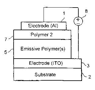
Figure; 1 shows ;chem;~tically the structure of the devices of the present
invention. 7"he devices of vthe present invention may be fabricated by spin
casting
polymer layers on one ele.cti°ode and then vacuum depositing the other
electrode. The
--4b-
CA 02279330 1999-07-29
WO 98/41065 PCT/US98/04831
spin casting technique is conventional and well-known in the art. However, a
wide
variety of other well known methods may also be used to obtain the layered
structure
shown in Figure 1 including doctor blading, dip coating, chemical vapor
deposition,
physical vapor evaporation, sputtering, and Langmuir-Blodgett techniques. Spin
casting is preferred due to the ease of fabrication and uniformity of the
resulting thin
films.
The CVBP devices of the present invention may operate under either polarity
of driving voltage with different colors of light being emitted under forward
and
reverse bias. The relative fast time response allows the rapid switch of
colors and AC
operation. The fundamental concept of the present invention is quite general,
it is
applicable to a variety of emitting materials in conjunction with suitable
redox
materials, as well as suitable electrode materials.
With respect to such alternative materials and referring to Figure 1, the
classical electron-injecting electrode 1 of either configuration (a), (b) or
(c) may be of
any appropriate material. The electrode materials may be metals, degenerate
semiconductors, and conducting polymers. Electrodes can be fashioned from any
suitable conductive material including electrode materials that may be metals,
degenerate semiconductors, and conducting polymers. Examples of such materials
include a wide variety of conducting materials including, but not limited to,
(1)
indium-tin-oxide ("ITO"), (2) metals such as gold, aluminum, calcium, silver,
copper,
indium and magnesium, (3) alloys such as magnesium-silver, (4) conducting
fibers
such as carbon fibers, and (5) highly-conducting organic polymers such as
highly-
5
SUBSTITUTE SHEET (RULE 26)
CA 02279330 1999-07-29
WO 98/41065 PCT/US98/04831
conducting doped polyaniline, highly-conducting doped polypyrrole, or
polyaniline
salt (such as PAN-CSA) or other pyridyl nitrogen-containing polymer, such as
polypyridylvinylene. Other examples may include materials that would allow the
devices to be constructed as hybrid devices through the use of semiconductive
S materials, such as n-doped silicon, n-doped polyacetylene or n-doped
polyparaphenylene.
In typical applications where the device is used for lighting and display, at
least one of the electrodes may be fashioned from a transparent material such
as
indium tin oxide or a partially transparent material such as highly-conducting
doped
polyaniline. Partially transparent electrodes may be used to advantage to
filter or clip
unwanted portions (frequencies) of light coming from the light-emitting
material.
It is noted that it is not necessary that the electrode material be
transparent or
even partially transparent. In cases where the electrode materials are opaque
to the
emitted light, light emission from the edge of the device may be utilized in,
for
example, coupling applications such as in coupling the device to an optical
fiber.
Since the devices of the present invention can be AC driven, it has the
advantage of
delivering modulated light output in frequency modulated or amplitude
modulated
form.
For ease of manufacture and safety purposes, it is often desirable to form
the device on a substrate which also serves to protect and often insulates
(both
physically and electrically) the device during use. The substrate layer may be
any
appropriate material; glass or clear electrically insulating plastic
substrates are
6
SUBSTITUTE SHEET (RULE 26)
r.
CA 02279330 1999-07-29
WO 98/41065 PCT/US98/04831
preferable when the device is used for lighting and display purposes. An AC
driven
device is especially suitable for light emission from both sides of the device
in which
case all of the insulating material and electrode materials are at least
partially
transparent as well as any protective substrates that may be used with one or
both
electrodes. The substrate layer is shown in Figure 1 as substrate layer 2.
The classical hole-injecting electrode 3 of either configuration (a), (b) or
(c)
may be of any appropriate high work function material, such as indium-tin-
oxide
("ITO"), gold (preferably transparent), or a polyaniline salt (such as PAN-
CSA).
Other electrode materials referred to as classical electron-injecting
electrode materials
may be used as the so-called hole-injecting electrode materials.
Other examples may include materials that would allow the devices to be
constructed as hybrid devices through the use of semiconductive materials,
such as p-
doped silicon, p-doped polyacetylene or p-doped polyparaphenylene.
With respect to the single layer embodiment (a) in Figure 1, the emissive
layer
of the single layer device (referred to in configuration (a) of Figure 1 as
the polymer
blend 4 may be any blend of at least two polymers; one polymer having
relatively
greater electron transporting properties and the other having relatively
greater hole
transporting properties. The same emissive layer is shown in the mufti-layer
configurations (b) and (c) of Figure 1, as emissive polymers) layer 5.
7
SUBSTITUTE SHEET (RULE 26)
CA 02279330 1999-07-29
WO 98/41065 PCT/US98/04831
Representative polymer blends of the emissive polymer layer may be selected
from several groups including, but are not limited to, conjugated and non-
conjugated
polymers and copolymers, including polypyridines, polypyridylvinylenes,
polythiophenes, polyphenylenes, polyphenylenevinylenes, rigid-rod polymers
such as
polyphenylenebenzobisthiozoles. polyfluorenes, polyvinylcarbazoles,
polythienylenevinylenes, emissive polycatylems and derivatives thereof and so
on. A
wide variety of specific materials (i.e., derivatives) can be found in each of
these
groups as a result of modifications to the basic structure. As an example, the
emissive
polymer layer may be a mixture of a polypyridylvinylene (i.e., having
relatively
greater electron transporting properties) and a polythiophene (i.e., having
relatively
greater hole transporting properties).
Both the emissive polymers) layer 5 (referred to in configuration (a) of
Figure
1 as the polymer blend 4) and redox polymers) layer 6 may be molecules,
oligomers,
polymer and copolymers with a variety of side groups, and blends of such above
I S materials.
In an alternative embodiment, devices in accordance with the present
invention may be constructed without a redox polymer as described in Figure 1
as
layer 6. Such devices have been shown to be operative. See Figure I (c) which
otherwise bears the same reference numerals as Figure 1 (b).
The emissive blend layer may also be fabricated from one or more such
polymers together with at least one molecular dopant {i.e., a non-polymeric
substance)
having hole- or electron-transport capability, so as to be capable of
affecting the hole-
or electron-transporting character of the emissive layer, thus affecting the
8
SUBSTITUTE SHEET (RULE 26)
CA 02279330 1999-07-29
WO 98/41065 PCT/US98/04831
recombination zone of this emissive layer. Such molecular dopants also may be
themselves light emissive under operative conditions. Examples of such
materials
include 8-hydroxy quinoline aluminum (A1Q3) (electron transporting; light
emissive),
2-(4-biphenylyl)-5-(4-tert-butylphenyl)-1,3,4-oxadiazole(PBD) (electron
transporting;
non-light emissive), N,N'-diphenyl-N,N'-bis(3-methylphenyl)-1,1'-biphenyl-4,4'-
diamine(TPD) (hole-transporting), 4,4'-bis[N-(1-napthyl)-N-phenyl-
amino]biphenyl
(a-NPD).
The Redox Polymer Laver
Representative redox material groups may include emeraldine base (E8) forms
of polyaniline, the sulfonated forms of the polyaniline ("SPAN"), and
derivatives of
these groups, and oligomers thereof. Salts of the sulfonated polyaniline, such
as those
formed with sodium hydroxide, may also be used. It is also noted that EB may
have a
range of imine unit concentration from 0.3 to 0.75 SPAN may have a range of
sulfonation 0.20 to in excess of 100%.
The A~jdic Redox Polymer Layer
The acidic redox polymer layer 7 may be any acidic polymer capable of
functioning in an electron/hole transport role. For instance, this polymer
layer may
comprise sulfonated polyaniline (SPAN) oligomers thereof, or polymers
containing
acid groups (i.e., acidic polymers), or polymers doped with an acid. For
instance, the
acidic polymer may comprise toluene sulfonic acid either incorporated into the
polymer itself or as a dopant of another polymer.
Llse of the Devices with Reversible Current
9
SUBSTITUTE SKEET (RULE 26)
CA 02279330 1999-07-29
WO 98/41065 PCT/US98/04831
It will be understood that the above-described components of the devices of
the present invention are described in classical terms, such as electron-
injecting and
hole-injecting electrodes, when referring to the devices as being operated in
the
classical forward direction. However, it will be recognized that when operated
in the
reverse direction, the classic roles of the above-described components are
reversed.
Accordingly, it will also be recognized that the devices of the present
invention may
also be operated with electrodes of either classical type alone or both
classical types.
The devices of the present invention may be operated by any appropriate
source of electrical energy 8 shown in Figure 1.
The light emitter of Figure 1 (a) is also in electrical contact with a first
electrode and a second electrode as described above, with the first and second
electrodes arranged in spaced relation with each other. The first electrode
and the
second electrode are electrically connected to a potential difference in
either direction.
That is. the first electrode can be connected to a positive potential (anode)
while the
second electrode is connected to a negative potential (cathode) or the
connections can
be reversed, with the first electrode connected to a negative potential while
the second
electrode is connected to a positive potential (opposite current direction).
Because the
device can be operated in either current direction with similar output
efficiency, it
allows the device to be driven with an alternating voltage, that is, the
device
preferably can be used with an alternating current.
The light emitter of Figure 1 (b) is in electrical contact with the polymeric
layers 6 and 7 which are, respectively, in electrical contact with electrodes
3 and 1.
SUBSTITUTE SHEET (RULE 2fi)
._w.__ .._
CA 02279330 1999-07-29
WO 98/41065 PCTNS98/04831
The first and second electrodes are electrically connected to a potential
difference as
described above with respect to Figure I(a).
The light emitter of Figure I(c) is in electrical contact with polymeric layer
7
and electrode 3; polymeric layer 7 in turn being in electrical contact with
electrode I.
The first and second electrodes are electrically connected to a potential
difference as is
described above with respect to Figure I (a).
The electrodes I and 3 are connected to a voltage source 8 by means of
suitable electrical connectors or contacts. Such electrical connectors and
contacts are
conventional in the art and may include wire leads, printed circuit
connectors, spring
clips. snaps, solder, wrapped posts, conducting glues, etc. It is also to be
understood
that the electrical connector or contact can be the electrodes 1 and 2
themselves. That
is, the potential difference from voltage source 8 may be applied directly to
the
electrodes in which case electrodes 1 and 3 may become the electrical contact
or
connector.
I ~ Although not limited to the theory of its operation, it is believed that
in
devices such as in the configurations shown in Figures 1 (b) and I (c), when
operated
in the forward direction, electrons encounter holes at about the interface of
the acidic
polymer layer 7 and the emissive polymer layer 5 causing emission of, for
instance,
red light; and, when operated in the reverse direction, electrons encounter
holes within
?0 the emissive polymer layer ~ causing emission of, for instance, green
light.
The devices of the present invention may be constructed as shown in Figure
1 (b) wherein layers 6 and 7 are the same acid group-coating polyaniline
materials.
Such devices due to differences in fabrication processing steps, are still
able to effect
11
SUBSTITUTE SHEET (RULE 26)
CA 02279330 1999-07-29
WO 98/41065 PCT/US98/04831
color variable operation. This is believed to be due to different degrees of
acid doping
of the emitting layer at the respective interface with each redox polymer
layer.
The devices of the present invention may feature a relatively low tum-on and
operating AC or DC voltage of less than about 24 volts. More preferably, a
turn-on
and operating voltage of less than about 12, less than about 6 volts, or even
less than
about 5 volts may been achieved. These low voltages make these devices
particularly
advantageous for use in toys, as commercial light strips such as found on-
airplanes
and in theaters, as signs, and as flat panel displays for computer and
television use.
The foregoing and other advantages of the invention will become apparent
from the following disclosure in which one or more preferred embodiments of
the
invention are described in detail and illustrated in the accompanying
drawings. It is
contemplated that variations in procedures, processing, structural features,
arrangement of parts, experimental design, ingredients, compositions,
compounds,
and elements may occur to a person skilled in the art without departing from
the scope
of or sacrificing any of the advantages of the invention.
fief Description of the Drawings
Figure 1 is a general schematic of the color variable bipolar light emitting
devices of the present invention, showing (a) single layer, (c) bilayer and
(b) trilayer
configurations.
Figure 2 shows the chemical structure of the repeating units of polymers that
may be used in accordance with one embodiment of the present invention.
Figure 3 is a graph showing the currentlvoltage/luminance characteristics and
corresponding electroluminescent spectra of the same device in accordance with
one
12
SUBSTITUTE SHEET (RULE 26)
r - _~.__ _
CA 02279330 1999-07-29
WO 98/41065 PCT/US98/04831
embodiment of the present invention, i.e., a color variable light emitting
device under
forward and reverse DC bias. The inset shows operation of the device under
both
classical forward and reverse operation.
Figure 4 is a graph showing the electroluminescent spectra of a single layer
color variable light emitting device under forward and reverse DC bias, in
accordance
with one embodiment of the present invention.
Figure 5 is a general schematic of a particular color variable bipolar light
emitting device in accordance with one embodiment of the present invention, as
described below.
Figure 6 is a graph showing the current-voltage and light-voltage
characteristics of a color variable light-emitting device under forward and
reverse bias
conditions; the inset shows the colors of the device under forward and reverse
bias in
the CIE chromaticity diagram.
Figure 7 is a graph showing the electroluminescent spectra of a multiple layer
color variable light emitting device under forward and reverse DC bias, in
accordance
with one embodiment of the present invention. Also shown are corresponding
electroluminescent spectra of the component polymers of the emitting layer.
Figure 8 is a graph showing the electroluminescent spectra of a multiple Iayer
color variable light emitting device under reverse DC bias, in accordance with
one
embodiment of the present invention, and showing the variability in color
dependent
upon the ratio of the polymer blend in the emissive layer.
Figure 9 is a graph showing an absorbance spectra from a PPyVPV film spin
cast from aqueous solution, and a bilayer of PPyVPV/SPAN; inset: absorbance
13
SUBSTITUTE SHEET (RULE 26)
CA 02279330 1999-07-29
WO 98/41065 PC'f/US98/04831
spectra as a result of the subtraction of the absorbance of each individual
layer from
that of the bilayer.
14
SUBSTITUTE SHEET (RUtE 26)
CA 02279330 1999-07-29
WO 98/41065 PCT/US98/04831
In accordance with the foregoing summary of the invention, the following
describes preferred embodiments of the present invention which are presently
considered to be the best mode of the invention.
In describing the preferred embodiments of the invention which is illustrated
in the drawings, specific terminology is resorted to for the sake of clarity.
However, it
is not intended that the invention be limited to the specific terms so
selected and it is
to be understood that each specific term includes all technical equivalents
that operate
in a similar manner to accomplish a similar purpose.
In this example, a color-variable light emitting device described
schematically
in Figure 5 comprises a copolymer of poly (pyridyl vinylene) and poly
(phenylene
vinylene) derivative, PPyVPV, and a copolymer of polythiophene and
polyphenylene
derivative, PTP, were used as the emitting materials (appearing as the
"Emitter" layer
in Figure ~); the emeraldine base (EB) form of polyaniline and the sulfonated
form of
polyaniline (SPAN) were used as the redox materials. ITO and A1 were used as
the
electrodes. The polymer layers were formed using spin coating techniques. The
EB
layer was first spin-coated at about 3000 rpm onto pre-cleaned patterned ITO
substrates (with a sheet resistance of 15 S2/0) from N-methylpyrrolidinone
(NMP)
solution (concentration of about 5 mg/ml). The emitting layer was then spin
coated
over the EB layer from a blend of PPyVPv and PTP (3:2 weight ratio) in xylenes
or
trichloroethylene (total concentration of about 10 mg/ml). Subsequently, the
SPAN
layer was coated over the emitting layer from an aqueous solution. All the
spin
SUBSTITUTE SHEET (RULE 26)
CA 02279330 1999-07-29
WO 98/41065 PCT/US98/04831
coating procedures were carried out inside a class 100 clean room. The top
metal
electrode was deposited by vacuum evaporation at a pressure below 10~ torr. To
prevent damage to the polymers, the substrate was mounted on a cold-water
cooled
surface during evaporation.
Absorption spectra were measured on spin-cast films using a Perkin-Elmer
Lamda 19 UV/VIS/NIR spectrometer. Photoluminesence (PL) and EL were measured
using a PTI fluorometer (Model QM-1). The current-voltage (I-V)
characteristics
were measured simultaneously with EL using two Keithly Model 195A multimeters
while the DC voltage was applied by a Hewlett-Packard Model 6218A DC power
supply. Quantum efficiency and brightness were measured using a calibrated
photodiode (UDT UV 100).
Figure 3 shows the typical current-voltage (I-V) and luminance-voltage
characteristics of the mufti-layer devices. The devices have typical turn on
voltages of
about 4 - 8 V, depending on film thickness, and work equally well under both
I 5 polarities of driving voltage with red light being emitted under forward
bias and green
light being emitted under reverse bias. The emitted light was clearly visible
under
normal indoor lighting. Internal device efficiencies of up to 0.1 %
photons/electron
has been achieved for the initial devices. The EL spectra under forward and
reverse
bias are shown in the inset of Figure 3. The CIE chromaticity x,y coordinates
of the
two colors are calculated to be (0.654,0.345) and (0.471,0.519), respectively,
showing
both colors to be relatively pure. The color of the devices can be switched
rapidly, up
to 20 kHz, depending upon pixel impedance and geometry.
16
SUBSTITUTE SHEET (RULE 26)
CA 02279330 1999-07-29
WO 98/41065 PCTIUS98/04831
Studies on the devices of the present invention show that the red light is
generated from the interface between the emitting layer and the SPAN layer
under
forward bias, and the green light is generated near the interface between the
emitting
layer and SPAN, in the bulk of the emitting layer, or at the interface between
the
emitting layer and the EB layer. The exact location and hence the color of the
light
generated can be varied by the ratio of the PPyVPV to PTP in the blend, i.e.
by the
overall charge transport properties of the emitting layer because the first
polymer, e.g.,
PPyVPV, has improved electron transport properties, and the second polymer,
e.g.,
PTP, has better hole transport properties.
The devices work under either polarity of driving voltage with different
colors
of light being emitted from different locations, red light from the emitting
polymer/SPAN interface under forward bias, and green light emitting from the
bulk of
the emitting polymers under reverse bias. Electroluminescence of the devices
peak at
550 nm with a shoulder at 585 nm under reverse bias while they show a single
peak at
665 nm under forward bias. The relative fast time response allows the rapid
switch of
colors and AC operation.
Figure 6 is similar to Figure 3 with the exception of the inset, showing both
colors to be relatively pure.
As shown in Figure 7, the EL spectra under forward bias is substantially
different from that of the single layer devices of either PPyVPV or PTP
suggesting
that the light is generated from the interface between the emitter blend and
either EB
or SPAN under forward bias. To further elucidate this effect, the following
devices
were fabricated: ITO/PPyVPV/Al; ITO/SPAN/PPpVPV/Al; ITO/PPyVPV/SPAN/AI;
17
SUBSTITUTE SHEET (RULE 2fi)
CA 02279330 1999-07-29
WO 98/41065 PCT/US98/04831
ITO/SPAN/PPyVPV/SPAN/AI and similar devices replacing SPAN with EB. All of
these devices were fabricated and tested under similar conditions in forward
bias.
Among all these devices, only ITO/PPyVPV/SPAN/Al and
ITO/SPAN/PPyVPV/SPAN/A1 show dramatically redshifted EL. This clearly
demonstrates that the red light is generated from the PPyVPV/SPAN interface on
the
cathode side under forward bias. Similar studies using PTP as the emitting
layer show
that the emission properties of PTP are not affected significantly by the
presence of
the SPAN layer.
The EL spectra of the color variable device under reverse bias are similar to
those of the single layer PPyVPV and PTP devices implying that the light is
generated
either in the bulk of the emitting polymer or at the EB interface. We are not
able to
identify the emission zone exactly because the EB layer does not modify the
emission
properties of the emitting polymer. The EB layer functions as a charge
injection
enhancement layer, playing a similar role as it does in symmetrically
configured AC
light-emitting (SCALE) devices reported earlier. Under reverse bias, the SPAN
layer
on the cathode side plays a similar role.
It is noted that when the blend in the color variable devices is replaced by
pure
PPyVPV polymers, the devices emit red light in forward bias and red-orange
light in
reverse bias. This indicates that, under reverse bias, the light is still
generated near
PPyVPV/SPAN interfaces. This can be understood in terms of different electron
and
hole transport properties of the PPyVPV and PTP polymers. Most conjugated
polymers, including poly(phenylene vinylene) (PPV) polyp-phenylene) (PPP) and
polythiophene, have better hole than electron transport properties. The
addition of a
18
SUBSTITUTE SHEET (RULE 26)
1 .. .~_.
CA 02279330 1999-07-29
WO 98/410b5 PC"r/US98/04831
high electronegativity unit, pyridine, to the backbone is expected to improve
the
electron transport properties. Therefore, under reverse bias the light is
still generated
near the SPAN interface for the ITO/EB/PPyVPV/SPAN/A1 device. By adding PTP,
which is expected to have better hole transport properties, to PPyVPV, the
overall
hole transport properties of the blend is improved, and hence the light is
generated
away from the SPAN interface for the ITO/EBBlend/SPAN/A1 device under reverse
bias, emitting green light. In fact, a gradual EL spectra shift toward green
has been
observed for the devices with increasing concentration of PTP in the blend, as
shown
in Fig. 8.
Initial studies suggest the formation of new emissive species due to
protonation of the pyridyi units by SPAN. This species was identified by both
absorption and PL experiments. Fig. 9 shows the absorbance spectra of a PPyVPV
layer, a SPAN layer, and a bilayer of PPyVPV/SPAN. SPAN is a self doped, water
soluble conducting polymer with a room temperature conductivity of 10'2 S/cm.
It
has a wide optical window from green to near IR. PPyVPV has an absorption band
peaked around 480 nm. An extra feature to the absorption at the interface is
clearly
shown in the inset of Fig. 9 as a result of subtraction of the absorbance of
each
individual layers from that of the bilayer. The interface absorption might be
attributed
to the new species as a result of protonation of PPyVPV by SPAN. One special
feature to SPAN is that it is acidic in aqueous solution and it is often
called
polyaniline sulfonic acid. On the other hand, the pyridyl unit is known to be
susceptible to protonation or quarternization by acid. To further clarify
this, the same
absorption experiment was performed on the films with the same configurations
as
19
SUBSTITUTE SHEET (RULE 26)
CA 02279330 1999-07-29
WO 98/41065 PCT/US98/04831
above but replacing the SPAN with toluene sulfonic acid (TSA). An almost
identical
absorbance feature to the PPyVPV/SPAN was found in the PPyVPV/TSA bilayer,
consistent with the new species at the PPyVPV/SPAN interface originating from
the
protonated pyridyl units. The new species are emissive and emit redshifted
light as
compared to non protonated polymer.
The color variable light-emitting devices described above have a number of
important advantages:
( 1 ) the two redox polymers modify the charge injection properties of the
polymer/metal interfaces which allows the use of high work function metals as
electrodes. This reduces the aging problems associated with "conventional"
polymer
LEDs which must use reactive low work function metals to achieve efficient
electron
injection;
(2) the introduction of the two redox polymers allows the devices to operate
in
both forward and reverse bias. Since no ionic species are involved directly in
the
device operation, the colors can be switched very rapidly, in sharp contrast
to
intrinsically slow response LECs.
(3) the emission zone is confined in between the two emitting polymer/redox
polymer interfaces which is away from the electrodes avoiding the EL quenching
effects near the metal electrodes; and
(4) the emitting polymers are protected by the redox polymers against direct
exposure to air, potentially improving the device stability.
SUBSTITUTE SHEET (RULE 26)
__ .~..~_.. J
CA 02279330 1999-07-29
WO 98/41065 PCT/US98/04831
Another approach to the color variable light-emitting device is represented by
single layer devices in which blends of two or more emitting materials with
different
emissive and charge transport properties are used as emitting layers.
Sometimes, one
or more non-emissive materials may be needed to control the overall properties
of the
emitting layer.
For an example of the single layer devices, a blend of the PPyV and PTP was
used as the emitting layer; ITO and A1 were used as electrodes. The emitting
layer
was formed by spin casting at 2000 rpm from solution in xylenes or
trichloroethylene
onto precleaned ITO substrate. An aluminum electrode was then deposited by
vacuum evaporation at a pressure below 10-6 torr. Figure 4 shows the EL
spectra of a
single layer device under forward and reverse bias. Different colors of light
were
generated under forward and reverse bias, although the color difference is
smaller than
that of the mufti-layer device.
I S The device of Example 2 was fabricated without layer 6, and wherein the
polyaniline layer 7 comprises SPAN, and the emissive polyaniline layer is a
blend of
the PPyVPV shown in Figure 2(a) and the PTP shown in Figure 2(b).
The concept of the color switchable light-emitting devices described here is
quite general, it can be applied to a variety of EL polymers in conjunction
with
suitable redox polymers. By including the blue emitters in the blend, color
variable
devices which generate other colors (including blue) are possible.
The preferred embodiments herein disclosed are not intended to be exhaustive
or to unnecessarily limit the scope of the invention. The preferred
embodiments were
21
SUBSTITUTE SHEET (RULE 26)
CA 02279330 2002-07-16
chosen and described in order to explain the principles of the present
invention so that
others skilled in the art may practice the invention. Having shown and
described
preferred embodiments of the present invention, it will be within the ability
of one of
ordinary skill in the art to make alterations or modifications to the present
invention,
such as through the substitution of equivalent materials or structural
arrangements, so
as to be able to practice the present invention without departing from its
spirit as
reflected in the appended claims. It is the intention, therefore, to limit the
invention
only as indicated by the scope of the claims.
-22-