Note: Descriptions are shown in the official language in which they were submitted.
CA 02279566 1999-08-03
TTTLE OF THE INVENTION
Receiver
BACKGROUND OF THE INVENTION
Field of the invention
The present invention relates to receivers and, more particularly, to a
receiver
which can perform tuning within a tuning band width related to a signal
frequency band
width for television broadcast.
Description of the prior art
The signal frequencies of television broadcast lie within a band width largely
different from that of the signal frequencies of radio broadcast. That is,
almost all the
television broadcast signals falls under a frequency band width of 6 MHz,
whereas the
radio broadcast signals are in a frequency band width as narrow as
approximately 100
kHz. Due to this, it has been a conventional practice to separately provide
receivers for
processing television and radio broadcast signals. In order to receive VHF
television
broadcasts, a television broadcast receiver la was required to include, as
shown in Figure
5, an input tuning circuit 2a, an RF amplifier 3a, an inter-stage tuning
circuit 4a, a mixer
Sa, a tuning circuit 6a, a local oscillation circuit 8a and an IF amplifier
7a. For receiving
FM radio broadcast, a radio broadcast receiver lb shown in Figure 6 was
required to have
the similar circuits 2b - 8b.
This however necessitate two circuits for each of signal processing, such as
in
tuning circuits and frequency conversion circuits, thus posing a problem of
spending cost.
SUMMARY OF THE INVENTION
Therefore, it is a primary object of the present invention to provide a
receiver
-1-
CA 02279566 1999-08-03
which can receive both television broadcast and radio broadcast.
A receiver according to the present invention, comprises: a tuning circuit
having a
first tuning band width; a first input terminal for inputting a first
broadcast signal having a
first frequency band width correlated to the first tuning band width; second
input terminal
for inputting a second broadcast signal having a second frequency band width
narrower
than the first frequency band width; an attenuation circuit for attenuating
signal
components of the second broadcast signal at around a desired channel; and a
selection
circuit for selecting and inputting to the tuning circuit one of the first
broadcast signal and
the second broadcast signal attenuated in the signal components.
According to this invention, inputted through the first terminal a first
broadcast
signal possessing a first frequency band width related to a first tuning band
width while
inputted through the second terminal a second broadcast signal having a second
frequency band width narrower than the first tuning band width. The selection
circuit
selects one of the first broadcast signal and the second broadcast signal
attenuated in
signal components, and inputs it to the tuning circuit having a first tuning
band width.
In one embodiment of the present invention, the attenuation circuit attenuates
the
signal components over the first frequency band width except for at the
desired channel.
Incidentally, the attenuation circuit includes a resonant circuit which
resonates at
frequency correlated to a tuning voltage.
In another embodiment of the present invention, the first broadcast signal is
a
television signal to be broadcast in a VHF band range, and the second
broadcast signal is
a radio signal to be FM broadcast in the VHF band range.
According to this invention, because attenuation is made for the second
broadcast
signal on signal components over the channel close to a desired channel, the
second
broadcast signal can be properly received even where the tuning means is broad
in tuning
-2-
CA 02279566 1999-08-03
band width. That is, proper reception is possible for both the first broadcast
signal and the
second broadcast signal.
The above described objects and other objects, features, aspects and
advantages of
the present invention will become more apparent from the following detailed
description
of the present invention when taken in conjunction with the accompanying
drawings.
BRIEF DESCRIPTION OF THE DRAWINGS
Figure 1 is an illustrative view showing one embodiment of the present
invention;
Figure 2 is an illustrative view showing part of operation in the Figure 1
embodiment;
Figure 3 is a chart showing frequency bands, picture frequencies, sound
frequencies and local oscillation frequencies for ground wave and CATV
channels
provided in the Japanese VHF band;
Figure 4 is a chart showing frequency bands, video frequencies, sound
frequencies
and local oscillation frequencies for ground wave and CATV channels provided
in the
U.S.VHF band;
Figure 5 is a diagram showing a prior art; and
Figure 6 is a diagram showing another prior art.
DETAILED DESCRIPTION OF THE PREFERRED EMBODIMENTS
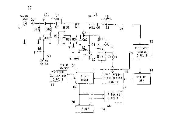
Referring to Figure l, a receiver 10 of this embodiment includes an input
terminal
S 1 to input a ground wave television broadcast signal and CATV broadcast
signal
(hereinafter referred collectively to as "VHF television broadcast signal") to
be broadcast
over a TV channel provided within the VHF band, and an input terminal S2 to
input a
radio broadcast signal to be FM-broadcast (hereinafter referred to as "FM
radio broadcast
-3-
CA 02279566 1999-08-03
signal") over a radio channel provided within the VHF band. Note that the VHF
band is
defined as a frequency band of from 30 MHz - 300 MFiz. Meanwhile, the input
terminal
S1 is connected with a television antenna (not shown) and the input terminal
S2 is with a
radio antenna (not shown).
The input terminal S1 is connected with one end of a capacitor Cpl. The
capacitor
Cpl has the other end connected with one end of a coil Lb grounded at the
other end as
well as one end of a capacitor Cb. The other end of the capacitor Cb is
grounded through
a coil Ld and capacitor Cd. The coil Ld and the capacitor Cd have a connection
point
grounded through resistors Rf and R6. Also, the resistors Rf and R6 have a
connection
point to which an input terminal S3 is connected to receive a control voltage.
The capacitor Cb at the other end is connected to one end of a coil Lh and an
anode
of a diode D1 through a parallel-connected coil Lf and capacitor C~ The diode
D1 has a
cathode that is grounded via a resistor R1 and also grounded through a
capacitor Cl. The
capacitor Cl has one end connected to one end of a capacitor Cp2 and an anode
of a diode
D2 through resistors R2 and R3. The resistors R2 and R3 has a connection point
grounded through a direct current power source V1, while the other end of the
capacitor
Cp2 is directly grounded at the other end. The coil Lh has the other end
connected to an
anode of a diode D3, and the diode D3 and the diode D2 are connected at their
cathodes
with each other.
The cathode of the diode D3 is connected to the input terminal S2 through the
capacitor C3. The capacitor C3 and the input terminal S2 has a connection
point that is
grounded through a coil L3. The cathode of the diode D3 is also grounded
through a coil
Ll and resistor R5. The coil Ll and the resistor RS has a connection point
that is
grounded through a capacitor C4 and parallel-connected variable diode Dv and
capacitor
C5. Further, the capacitors C4 and CS has a connection point that is connected
to a
-4-
CA 02279566 1999-08-03
tuning-voltage input terminal S4 through a resistor R4. Also, the coil Lh has
the other end
connected to a VHF input tuning circuit 12 through a capacitor C6 and parallel-
connected
coil L2 and capacitor C7.
The capacitors Cpl and Cb as well as the coil Lb constitute a high-pass filter
which removes direct-current and low-frequency components as other portions
than a
VHF television broadcast signal having been inputted through the input
terminal S1. The
capacitor Cb and coil Lb also cooperate with the coil Ld and capacitor Cd to
form a n -
type high-pass filter, which removes Cb wireless signals. The coil Lf and
capacitor Cf
form an FM trap circuit so that this FM trap circuit 22 can trap an FM radio
broadcast
signal broadcast over a radio channel adjacent to a TV channel. That is, in
Japan ground
wave television broadcast is implemented within a frequency band of 90 MHz -
222 MHz
while FM radio broadcast is within a frequency band of 76 MHz - 90 MHz. Due to
this,
the coil Lf and capacitor Cf apply a trap to an FM radio broadcast signal in
order not to
contain noise when selecting a TV channel.
On the other hand, the capacitor C3 and coil L3 connected to the input
terminal S2
form a high-pass filter to thereby remove direct-current and low-frequency
components
as other portions than an FM radio broadcast signal. Also, the coil Ll,
resistors R4 and
R5, capacitors C4 and CS and variable capacitance diode Dv constitute a trap
circuit 24
for reducing a band width. The variable capacitance diode Dv has a capacitance
value
controlled by a tuning voltage, thereby varying the resonant frequency. The
capacitor C4
is provided to cut off a cathode voltage of the variable capacitance diode Dv
and a
cathode voltage of the diodes D2 and D3 from each other, and has a large
capacitance
value. Due to this, the capacitance of the capacitor C4 is negligible at high
frequencies.
Consequently, provided that the capacitance value of the variable capacitance
diode Dv is
Cv, the resonant frequency Ft to be defined by the coil Ll, capacitor CS and
variable
-5-
CA 02279566 1999-08-03
capacitance diode Dv is expressed by Equation 1.
[Equation 1)
Ft = 1 / (2 n,/- {Ll * (Cv + CS)}]
At a resonant frequency Ft, the trap circuit 24 is decreased in impedance so
that a
frequency component containing a resonant frequency Ft is allowed to flow
through the
trap circuit 24 to a ground surface. Consequently, attenuated are unwanted-
channel FM
radio broadcast signals at around the resonant frequency Ft as a center.
Incidentally, the
capacitor CS is provided to correct for the resonant frequency.
The capacitor C6 is selectively inputted by a VHF television broadcast signal
or an
FM radio broadcast signal, in response to a control voltage applied to the
input terminal
S3. During receiving a VHF television broadcast signal, the input terminal S3
is given a
control voltage of 0 volt. This decreases respective anode voltages of the
diodes D1 and
D3 lower than their cathode voltages. That is, the diode D 1 at its cathode is
connected to
the direct current power source Vl through the resistor R2. The diode D3 at
its cathode is
connected to the direct current power source Vl through the diode D2 and
resistor R3.
Further, the diode DZ at its cathode is grounded through the coil Ll and
resistor R5.
Accordingly, if the resistor Rf as well as the resistors R1- R3 and RS are set
to proper
resistance values, the diodes D1 and D3 become a non-conductive state while
the diode
D2 becomes a conductive state, in response to a 0-volt control voltage. Due to
this, the
FM radio broadcast signal flows through the diode DZ and capacitor Cp2 to the
ground
surface. On the other hand, the VHF television broadcast signal having passed
through
the FM trap circuit 22 is given to the capacitor C6 through the coil Lh.
Incidentally, the
coil Lh is set in order to attenuate higher frequencies than the VHF band.
During FM radio broadcast reception, a plus control voltage higher than the
direct
current power source V1 is applied to the input terminal S3. At this time, the
diodes D1
-6-
CA 02279566 1999-08-03
and D3 become a conductive state while the diode D2 becomes a non-conductive
state.
Consequently, the VHF television broadcast signal having passed through the FM
trap
circuit 22 flows through the diode D1 and capacitor C1 to the ground surface.
Meanwhile, the FM radio broadcast signal is given to the capacitor C6 through
the diode
D3. At this time, the coil Lh plays a role to block the VHF television
broadcast signal
from flowing toward the capacitor C6. The diode D2 also plays a role to
prevent the FM
radio broadcast signal from flowing toward the capacitor Cp2. As a
consequence, the coil
Lh may be replaced with a diode, and the diode D2 may be replaced by a coil.
These
diodes D1- D3 and coil Lh operate as an analog switch 26 to select one of a
VHF
television broadcast signal and an FM radio broadcast signal.
The capacitor C6 cut off the direct current component included in a VHF
television broadcast signal or FM radio broadcast signal. Meanwhile, the coil
L2 and
capacitor C7 forms an IF (Intermediate Frequency) trap circuit 28 which traps
an IF
component contained in a VHF television broadcast signal or FM radio broadcast
signal.
Any of the broadcast signals having passed through the capacitor C6 and IF
trap circuit 28
is given to a VHF input tuning circuit 12 having a tuning band of
approximately 6 MHz.
As will be understood from Figure 3, in Japan all the channels included within
the
VHF band (ground wave TV and CATV channels) possess a frequency band width of
6
MHz. On the contrary, the FM radio channels though not shown have a frequency
band
width of as narrow as 100 KHz. Consequently, if an FM radio broadcast signal
be
inputted as it is to the VHF input tuning circuit 12, tuning is applied to
over unwanted FM
radio channels thereby making it impossible to listen to an FM radio
broadcast.
Therefore, this embodiment is provided with the trap circuit 24 in order to
remove signals
to be broadcast over the channels adjacent to a desired FM radio channel. By
properly
setting an inductance value for the coil Ll and capacitance values for the
capacitor C5
CA 02279566 1999-08-03
and variable capacitance diode Dv, the VHF input tuning circuit 12 can apply
tuning only
to a desired TV channel or radio channel.
As understood from Figure 2, the tuning band has a band width of 6 MHz. The
trap circuit 24 applies trapping to a lower frequency band than a selected FM
radio
channel, responsive to a tuning voltage. That is, the signal components within
this
frequency band attenuate due to resonance by the resonant circuit formed by
the coil Ll,
capacitor CS and variable capacitance diode Dv. The trap band width at this
time is
approximately 5.9 MHz. The VHF input tuning circuit 12 sets a tuning range
such that a
selected FM radio channel comes to an upper end of a tuning range.
Consequently, only a
selected-channel FM radio broadcast signal is outputted from the VHF input
tuning
circuit 12. Thus, reception is for only a desired-channel FM radio signal,
even where the
VHF input tuning circuit 12 is broad in tuning band.
Incidentally, the VHF input tuning circuit 12 is given a band switching
voltage VH
or V~. For a band switching voltage VH, the VHF input tuning circuit 12
effects tuning in
a VHF band of 170 MHz or higher, i.e. in a VHF band range of Japanese ground
wave
channel "4" or greater. Meanwhile, for a band switching voltage V,, the VHF
input
tuning circuit 12 effects tuning in a VHF band range of 170 MHz or lower, i.e.
in a VHF
band range of CATV channel "C22" or smaller.
The VHF television broadcast signal or FM radio broadcast signal tuned by the
input tuning circuit 12 is thereafter amplified by an RF amplifier 14 so that
an amplified
signal is supplied through a VHF inter-stage tuning circuit 15 to a VHF mixer
16. The
signal is subjected to frequency conversion by the VHF mixer 16 to provide an
IF signal.
Incidentally, the VHF input tuning circuit 12, the VHF inter-stage tuning
circuit 15 and
the VHF local oscillation circuit 17 operate responsive to a tuning voltage.
The VHF mixer 16 outputs not only an IF signal as a differential signal
between a
_g_
CA 02279566 1999-08-03
broadcast signal and a local oscillation signal but also a sum signal of the
broadcast signal
and the local oscillation signal. Accordingly, an IF tuning circuit 18
extracts only the ff
signal and supplies it to an IF amplifier 20. The IF signal amplified by the
IF amplifier 20
is outputted through an output terminal S5. Incidentally, the receiver 10
constructed as
above is accommodated within a case having an outside size standardized by
IEC.
In this embodiment, for an FM radio broadcast signal the trap circuit 24
causes
attenuation in other frequency components than that of a desired channel.
Consequently,
even if the VHF input tuning circuit 12 is broad in tuning band, it is
possible to carry out
tuning to a desired FM radio channel. That is, this embodiment can use a
common circuit
to receive VHF television and FM radio broadcasts, thus achieving cost
reduction.
For reference, in U.S.A. ground wave and CATV channels are in the VHF band, as
shown in Figure 4. Also, FM radio channels each having a band width of
approximately
200 kHz are provided within a frequency band of from 88 MHz - 108 MHz. Due to
this,
if the receiver 10 of this embodiment is to be used in U.S.A., the trap band
of the trap
circuit 24 should be changed. Incidentally, although the FM radio channels
partly
overlap with the CATV channels, there is no especial problem because the
television
broadcast signal is inputted through the input terminal S 1 while the radio
broadcast signal
is inputted through the input terminal S2.
Incidentally, this embodiment inputted the FM radio broadcast signal and the
VHF
television broadcast signal through different input terminals from each other.
Alternatively, the input terminals may be commonly connected to an antenna
that can
receive both FM radio broadcast and VHF television broadcast. Also, in this
embodiment
the input terminal S1 inputted only a VHF television broadcast signal.
Alternatively, the
input terminal S1 may be arranged to input a ground wave broadcast signal and
CATV
broadcast signal (UHF television broadcast signal) to be aired over a channel
provided in
-9-
CA 02279566 1999-08-03
a UHF band. In this case, there is necessity to provide an input tuning
circuit, RF
amplifier, inter-stage tuning circuit, mixer, IF tuning circuit and IF
amplifier to process
UHF television broadcast signals.
Although the present invention has been described and illustrated in detail,
it is
clearly understood that the same is by way of illustration and example only
and is not to
be taken by way of limitation, the spirit and scope of the present invention
being limited
only by the terms of the appended claims.
- 10-