Note: Descriptions are shown in the official language in which they were submitted.
CA 02279582 1999-08-16
SYSTEM MONITORING REPROGRAMMABLE
IMPLANTABLE TRANSPONDER AND METHOD
OF CALIBRATING SAME
BACKGROUND OF THE INVENTION
This invention is directed to a passive transponder, and, in
particular to a passive transponder which is reprogrammable after
completion of manufacture (and insertion in the host) and is
utilized for monitoring characteristics of the host to which it is
imbedded, and more in particular for identifying an animal and its
characteristics.
Transponders and scanner systems are well known in the art.
These systems include an interrogator which transmits and receives
signals from a passive transponder. One such use is a transponder
implanted in an animal. U.S. Patent No. 5,252,962 describes a one
time programmable EEPROM that can store an identification code that
corresponds to the identification of the animal in which it is
imbedded. It is also known in the art to reprogram a transponder
utilizing an EEPROM or the like. However, the prior art
transponders have been less than completely satisfactory because
they provide little or no information to the interrogator to ensure
proper programming. Accordingly, in a contemplated use such as
animal identification, transponders have been unable to reliably
indicate to the interrogator that the data is being properly stored,
changed or deleted within each transponder.
Also, heretofore transponders have had circuitry designed to
measure the temperature of the animal in which it is implanted. One
such analog circuit described in U.S. Patent No. 5,252,962 has been
less than accurate. Therefore, it is desirable to provide a passive
transponder which overcomes the shortcomings of the prior art,
indicates to an interrogator whether sufficient power is being
received in order to be programmed, senses an environmental
condition, such as the temperature of the host animal, transmits
this information along with other host information to an
CA 02279582 1999-08-16
2
interrogator and can perform an essentially simultaneous exchange
of information with the interrogator.
SUMMARY OF THE INVENTION
Generally speaking, in accordance with the instant invention,
a passive transponder is provided, the transponder including an
antenna for receiving an input signal to power the transponder, the
signal also containing data and commands from the signal source and
being also capable of transmitting an output signal to the signal
source. The transponder also includes memory for storing data
received by the transponder from the signal source, the transponder
operating in either a READ mode for outputting information from the
transponder to the signal source, or in a PROGRAMMING mode wherein
the memory stores data in response to information contained in the
input signal. The transponder also includes an integrity circuit
for indicating to the signal source that sufficient power is
available from the signal source for causing the memory to store
the data. The transponder also includes a monitoring circuit for
monitoring a characteristic of a host. The memory includes a
plurality of memory storage locations, with locations addressed
sequentially to read data stored in the memory and with addressing
occurring at a rate which is a submultiple of the signal source
frequency. The monitoring circuit monitors the characteristic
during the period of time required to address a predetermined
number of the addresses of the memory. The transponder also
includes an impedance modulator for permitting substantially
simultaneous two way communication between the transponder and
signal source.
Also provided is a method of calibrating a transponder so that
a user or programmer can receive accurate temperature information
about the host in which the transponder is embedded. The method
includes the steps of placing the transponder in a liquid bath
having a known temperature, computing the temperature of the liquid
bath based on the output signal outputted by the transponder,
comparing the computed temperature with the known temperature to
CA 02279582 1999-08-16
3
obtain a temperature difference and storing the difference between
the computed temperature and the known temperature (offsett,sp
value) in a predetermined memory location of the transponder.
Once embedded in the host, an accurate temperature reading of
the host may be ascertained by adding the offsett,mp value stored in
the transponder to the temperature data outputted from the
transponder as a portion of the output signal. The sum total of
the offsett,mp value and the temperature data outputted by the
transponder may also be displayed to the user.
Accordingly, it is an object of the instant invention to
provide an improved passive transponder.
A further object of the invention is to provide a passive
transponder which senses and transmits the characteristic of an
object into which it has been imbedded.
Another ob ject of the invention is to provide a reprogrammable
passive transponder capable of providing information to the
interrogator to indicate that sufficient power is being received
to program the transponder.
Yet another object of the instant invention is to provide an
improved passive transponder for more accurately determining and
communicating the temperature of a host.
A further object of the invention is to use phase modulation
to more accurately transmit data to the interrogator.
Still another object of the invention is to utilize an
impedance modulator to allow for essentially simultaneous
transmission and reception of data with the interrogator having a
passive design.
Another object of the invention is to improve circuit
efficiency by utilizing common circuits to perform different
functions in both read and program modes.
Yet another object of the invention is to provide a
transponder which collects host characteristic data while reading
data from the memory.
Another object of the invention is to improve circuit
efficiency and performance by using a clock frequency and timing
CA 02279582 1999-08-16
4
signals derived from, and locked to, the frequency of the signal
source.
Another object of the invention is to improve data .
transmission rates by accomplishing measurement of host
characteristics during transmission of stored information.
Another ob ject of the present invention is to provide a method
of calibrating a transponder to more accurately display the
temperature characteristic of the host in which the transponder is
embedded.
Yet another object of the invention is to utilize a passive
transponder memory in combination with an on-board characteristic
sensor to provide an accurate measurement of the characteristic.
Another object of the invention is to provide circuitry to
prevent inadvertent over-writing of any portion of the stored data.
Another object of the invention is to provide circuitry to
provide selective over-writing of stored data.
Another object of the invention is to provide circuitry
requiring a coded command to enter the program mode and thus
prevent false programming.
Still other objects and advantages of the invention will in
part be obvious and will in part be apparent from the
specification.
The invention accordingly comprises the several steps and the
relation of one or more of such steps with respect to each of the
others thereof, which will be exemplified in the method hereinafter
disclosed, and the scope of the invention will be indicated in the
claims.
BRIEF DESCRIPTION OF THE DRAWINGS
For a fuller understanding of the invention, reference is had
to the following description taken in connection with the
accompanying drawings, in which:
FIG. 1 is a block circuit diagram of a passive transponder
constructed in accordance with a preferred embodiment of the
instant invention;
CA 02279582 1999-08-16
FIG. 2 is a block circuit diagram of an address and timing
generator constructed in accordance with the invention;
FIG. 3 is a circuit diagram of a temperature clock-master
clock selector constructed in accordance with the instant
invention;
FIG. 4 is a circuit diagram of a data sequence generator
constructed in accordance with the instant invention;
FIG. 5 is a circuit diagram of a mode decoder constructed in
accordance with the instant invention;
FIG. 6 is a circuit diagram of a phase modulator constructed
in accordance with the instant invention;
FIG. 7 is a circuit diagram of an impedance modulator
constructed in accordance with the instant invention;
FIG. 8 is a circuit diagram of a Manchester encoder and
preamble generator in accordance with the present invention;
FIG. 9 is a side elevation view of a passive transponder
constructed in accordance with the instant invention;
FIG. 10 is a top plan view of a passive transponder
constructed in accordance with the instant invention;
FIG. 11 is a bottom plan view of a passive transponder
constructed in accordance with the instant invention;
FIG. 12 is a cross-sectional view taken along line 12-12 of
FIG. 11;
FIG. 13 is a cross-sectional view taken along line 13-13 of
FIG. 11; and
FIG. 14 is a block circuit diagram of an interrogator and
passive transponder in accordance with the present invention.
DETAILED DESCRIPTION OF THE PREFERRED EMBODIMENTS
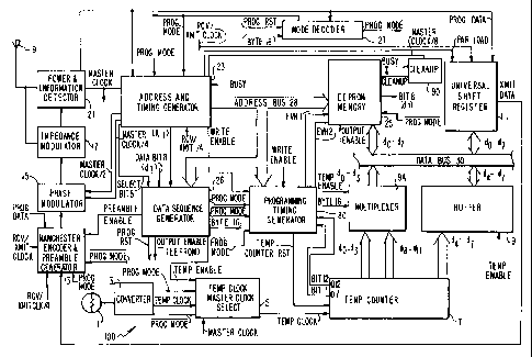
Reference is first made to FIG. 1 in which a block diagram of
an implantable passive transponder ("transponder"), generally
indicated as 100, is provided. Transponder 100 may be placed, for
example, under the skin of a laboratory animal, such as a rodent.
In an exemplary embodiment, transponder 100 communicates with
an interrogator 1000, as shown in FIG. 14, through inductive
' CA 02279582 2005-04-13
6
coupling generally known in the art from U.S. Patent No. 4,730,198.
Interrogator
1000 includes the structures as disclosed in U.S. Patent No. 5,250,944. A
signal at
a selected frequency is received from the interrogator by single coil antenna
19.
This frequency is the MASTER CLOCK frequency for the transponder. In the
exemplary embodiment described herein the MASTER CLOCK frequency is about
364 Khz. The waveform of the signal source can also contain data and control
information to be sent to the transponder.
Transponder 100 will remain in the OFF state, until a signal of a sufficient
power level is received by transponder 100 from the interrogator. The
interrogator,
which may be a handheld device, may also contain an adjustable exciter that
controls, along with the distance between the interrogator and the
transponder, the
signal level to the transponder. When the interrogator transmits a signal of
sufficient power to transponder 100, the transponder is placed in an "ON"
state and
can transmit data to, or receive data from, the interrogator. As will be
explained in
detail below, receipt and storage of data is only possible after the
transponder has
returned to the interrogator a signal indicating the transponder 100 has
received a
signal of sufficient voltage level to permit storage of data and the
interrogator has
responded with a command to enter the program mode. As will also be explained
below, transponder 100 transmits data to an interrogator in a READ mode and
receives and stores data from the interrogator in the PROGRAM mode.
To facilitate an understanding of FIG. 1, transponder 100 is initially
described
after transponder 100 has been programmed and after a user selected
identification
code has been stored in an electrically erasable programmable read only memory
25 ("EEPROM 25").
With reference to FIG. 1, single antenna is provided both
a 19 for
communication with,and receivingpower from, the interrogator.Upon
receipt of a signal of suitable power level,
CA 02279582 1999-08-16
7
transponder 100 turns ON and enters the read mode and transmits
data to the interrogator. The signal from antenna 19 is fed to a
power and information detection circuit 21. The power and
information detection circuit includes a full wave bridge
rectifier. Detector 21 provides do power for transponder 100,
detects the envelope of the signal from which is established the
PROG DATA signal, and generates the MASTER CLOCK signal by squaring
up a half wave rectified portion of the signal received by antenna
19. Detection circuit 21 also includes the necessary overvoltage
protection and level references needed for proper operation of the
transponder. The PROG DATA signal is applied to a mode decoder
circuit 27. Depending on the data, carried by the PROG DATA signal
the transponder will remain in the READ mode or will be placed in
the PROGRAM mode by outputting the associated PROG MODE and
PROG MODE signals.
An address and timing generator 23, including dividers 70a,
70b (FIG. 2), receives the 364 KHz MASTER CLOCK signal from the
power and information detection circuit 21 and through dividers 70a
and 70b and associated logic gates, develops a number of timing and
address signals: The TRANSMIT CLOCK and RECEIVE CLOCK signals are
developed in divider 70a and both are fed to MUX 70 where MUX 70
selects, based on the status of the PROG MODE and PROG MODE lines,
either the TRANSMIT CLOCR or the RECEIVE CLOCR for input to divider
70b as well as input to other blocks via the RCV/XMIT clock line,
MASTER CLOCK divided by 2 and MASTER CLOCK divided by 4 signals are
also developed in divider 70a and are used to develop 91 KHz signal
in phase and a 9lRHz out of phase (90 degrees out of phase) to be
used by phase modulator 15 for encoding data to be transmitted back
t~ the interrogator. The Ao-A3 outputs of divider 70b, whose input
is either the RECEIVE CLOCK or the TRANSMIT CLOCK, is used to
sequentially addresses the bytes of EEPROM 25 via address bus 28.
The bit address signals A-1 through A-3 signals are also outputs of
divider 70b and are used to identify the first and eighth bit of
each byte and the period of time when the first 4 bits of the data
stored in byte 15 of EEPROM 25 could be transmitted but are in fact
replaced with a preamble.
CA 02279582 1999-08-16
8
Reference is again made to FIG. 1 wherein universal shift
register 11 is depicted. Shift register 11 receives data from a
data bus 30 for output during the READ mode. Address and timing
generator 23 applies a PAR LOAD signal to shift register 11. When
the PAR LOAD signal is high and the TRANSMIT CLOCK signal
transitions from a low to high state during the first bit of every
eight bit sequence; either stored data from EEPROM 25 or
temperature data (described below) via buffer 9 or data multiplexer
9a is placed on data bus 30. During the READ mode, shift register
11 serially outputs the data to a preamble generator and Manchester
encoder and preamble generator 13 ("encoder and preamble generator
13"). Encoder and preamble generator 13, in response to a PROG
DATA signal, TRANSMIT CLOCK signal, and a divided TRANSMIT CLOCK
signal, encodes the serial data received from shift register 11,
generates a preamble and outputs the preamble and Manchester
encoded data to phase modulator 15.
Phase modulator 15, using the MASTER CLOCK/2 signal and MASTER
CLOCK/4 signal from address and timing generator 23 generates an
in phase signal and out of phase signal necessary to encode the
data appearing on the transmit data line. Phase encoding occurs
in phase modulator 15 as the data on the line selects, via a
multiplexes 55 (FIG. 6), the appropriate in phase or out of phase
signal. Phase modulator 15 outputs the phase encoded data to
impedance modulator 17.
Impedance modulator 17 modulates the apparent impedance of
antenna 19 by selectively placing a load resistance across the
antenna, at timing intervals that are determined by the signal
received from antenna 19 and the phase modulated, Manchester
encoded data. The changing load impedance across antenna 19 is
what is sensed by the interrogator as the receive signal.
A thermistor 1 changes its resistance in response to
temperature. A converter 3, controlled by thermistor 1, provides
an output signal TEMP FREQ. The frequency of TEMP FREQ signal from
temperature to frequency converter 3 ( "converter 3" ) is a function
of the temperature sensed by thermistor 1. A temperature clock-
master clock selector 5, receives as a first input a TEMP ENABLE
CA 02279582 1999-08-16
9
signal from a data sequence generator 26, either a PROG MODE signal
a MASTER CLOCK signal and a TEMP FREQ signal. Selector 5 selects
which of these signals will be upheld binary counter 7. In an
exemplary embodiment, In the READ mode, counter 7 counts the
positive going transitions in the TEMP CLOCK signal produced at the
output of converter 3 (TEMP FREQ) during the timing interval the
first 14 bytes from the EEPROM are being transmitted to the
interrogator. As noted above, buffer 9 and data multiplexes 9a
selectively couple the temperature data in counter 7 to data bus
30. Also as noted, the temperature data on data bus 30 is parallel
loaded into shift register 11 and then serially outputted to
Manchester encoder and preamble generator 13.
Data sequence generator 26 establishes when in the transmit
cycle of the READ mode the information stored in EEPROM 25 (via the
OUTPUT ENABLE signal), the preamble ( via the PREAMBLE ENABLE
signal) and the temperature (via the TEMP ENABLE signal) are
transmitted to the interrogator. The TEMP ENABLE signal controls
the input to the temperature counter 7 when not in the PROGRAM mode
via the temp clock- master clock selector 5. Data sequence
generator 26 also identifies byte 16 (via the BYTE 16 signal) to
allow the circuitry of mode decoder 27 to look for the command
sequence that places the transponder in the program mode and
provides the PROG RST signal that permits mode decoder 27 to look
for the command sequence only if data bit 8 of the 16th byte stored
in EEPROM 25 is not a zero.
The PREAMBLE ENABLE signal input to encoder and preamble
generator 13 permits encoder 13 to apply a non-Manchester encoded
preamble signal which indicates both transponder timing and the
whether the voltage level on the PROG DATA line is above or below
approximately 3 volts, i.e., sufficient to program transponder 100.
Provided that transponder 100 is receiving sufficient power to
remain ON, it remains in the READ mode unless and until it is
placed in the PROGRAM mode. A predetermined pulse sequence on the
PROG DATA line will place transponder 100 in the PROGRAM mode but
this sequence should not be sent from the interrogator unless the
transponder has notified the interrogator that the signal power
CA 02279582 1999-08-16
level is adequate for programming EEPROM 25. The PROG DATA line
is fed to mode decoder circuit 27 which decodes the sequence to
determine if the command to enter the program mode has been
received.
In the PROGRAM mode, data from the interrogator appears on the
PROG DATA line, is clocked into the universal shift register 11
using the RECEIVE CLOCK signal, and then output parallel outputs,
and therefor onto the data bus 30 and the input/output lines (d0-
d7) of EEPROM 25. The clock signal of universal shift register
11 is the signal on the RCV/XMIT line and, is selected by MUX 70
(FIG. 2) when transponder 100 is in the PROGRAM mode. Once the
eight bits of data are on data bus 30, address and timing generator
23 outputs a WRITE ENABLE signal to Programming Timing Generator
80.
Programming-timing generator 80, in response to the WRITE
ENABLE signal, provides signals to EEPROM 25 to control the timing
of the write cycles therein. During the write cycle, the busy
output of EEPROM 25 disables divider 70a of address and timing
generator 23 by removing the MASTER CLOCK input thus stopping the
RECEIVE CLOCK and therefor preventing the EEPROM address from
changing. Also during the write cycle, the temperature clock-
master clock selector 5, which is also receiving the MASTER CLOCK
and the TEMP FREQ, selects the MASTER CLOCK for input to counter
7 which provides the timing functions for the writing of data into
EEPROM 25. After each byte is written to EEPROM 25, a clean-up
circuit 90 is provided to enable EEPROM 25 to receive a subsequent
byte of data in response to the MASTER CLOCK and a Busy signal from
EEPROM 25 (FIG. 2).
READ MODE
When transponder 100 is "powered up", it defaults to the READ
mode. Accordingly, immediately upon receiving sufficient power,
and while transponder 100 is in the READ mode, transponder 100 will
transmit three distinct types of data: the temperature of the
animal in which the transponder is embedded; data stored in EEPROM
25, usually identification data for the animal; and a preamble that
indicates the voltage level received by the transponder 100 and
CA 02279582 1999-08-16
11
sets up a timing reference for the interrogator. The transmission
of this data (preamble, temperature data, identification data) by
transponder 100 is continually repeated as long as the signal
transmitted by the interrogator provides sufficient power to the
transponder and a command to enter the PROGRAM mode is not sent
from the interrogator.
In a preferred embodiment, the preamble is followed by the
temperature data and thereafter followed by the identification data
stored in EEPROM 25. The temperature data contains information
conveying the body temperature of the animal in which the
transponder is embedded. Thereafter, and until the transponder is
placed in the program mode or insufficient power is received by the
transponder, the entire data stream will be continuously repeated.
Reference is again made to FIG. 2 to specifically describe the
circuitry of transponder 100 for transmitting the above-mentioned
data to the interrogator. Providing the various clock signals is
the function of address and timing generator 23. Address and
timing generator 23 includes an OR gate 240 which receives the 364
RHz MASTER CLOCK signal from power and information detection
circuit 21 and a BUSY signal from EEPROM 25 and in the absence of
a Busy Signal outputs the MASTER CLOCK to divider 70a. Dividers
70a and 70b and MUX 70, develop a number of timing and address
signals : The TRANSMIT CLOCK and RECEIVE CLOCR signals are developed
in divider 70a and both are fed to MUX 70 where MUX 70 selects
either the TRANSMIT CLOCK or the RECEIVE CLOCR for input to divider
70b as well as input to other blocks in response to PROG MODE.
MASTER CLOCK/2 and MASTER CLOCK/4 signals are also developed in
divider 70a and are used to develop a first 91KHZ signal, and a
second 91RHZ, 90 degrees out of phase with the first signal phase
modulator 15 for encoding data to be transmitted back to the
interrogator. The A.fl-A3 outputs of divider 70b, whose input is
either the RECEIVE CLOCK signal or the TRANSMIT CLOCK signal, is
used to sequentially address the bytes of EEPROM 25 via address bus
28.
Address and timing generator 23 also includes an AND gate 24b
receiving the A-1, A-2, and signals on the RCV/XMIT line as inputs
CA 02279582 1999-08-16
12
and produces a Select Bit 8 signal. An AND gate 242 receives PROG
MODE, PROG DATA and Select Bit 8 signals as inputs and produces an
WRITE ENABLE signal. An AND gate 244 receives the A1-A-3 signals
as inputs and produces a Bit 1 signal. An AND gate 248 receives
an inverted PROG MODE signal and the Bit 1 signal produces the PAR
LOAD signal. As a result, the bit address signals A-1 through A-3
signals and the output signals of divider 70b are used to identify
the first and eighth bit of each byte. The appropriate clock is
selected by MUX 70 based on the status of the PROG MODE and not
PROG MODE signals.
With reference to Fig 1, EEPROM 25 preferably has 16
addressable bytes, each being addressable by address and timing
generator 23 via address bus 28, specifically, output signals and
Ao-A3 the four high order bits of divider 70b. The OUTPUT ENABLE
produced by data sequence generator 26 goes high permitting EEPROM
25 to output its data, and when low tri-states the output of EEPROM
25 so as not to conflict with data from buffer 9 and multiplexer
9A. In the preferred embodiment, address and timing generator 23
sequentially addresses the addresses of EEPROM 25. As each address
of EEPROM 25 is addressed in the READ mode, the data stored at that
address is output onto data bus 30 and shifted out to the encoder
and preamble generator 13. The loading of the data into shift
register 11 will next be described.
At the end of 8 clock pulses of the MASTER CLOCK, the data on
bus 30 is parallel loaded into shift register 11 when the high
level on the PAR LOAD signal line from address and timing generator
23 is clocked into universal shift register 11 by a low to high
transition of the TRANSMIT CLOCK appearing on the RCV/XMIT signal
line from address and timing generator 23. Thereafter the data in
shift register 11 is outputted serially to encoder and preamble
generator 13 at the TRANSMIT CLOCK rate of - 11 Khz (MASTER
CLOCK/32).
The PREAMBLE ENABLE signal output of data sequence generator
26 indicates when the first half of data byte 15 could be
transmitted, and forces encoder and preamble generator 13 to insert
the 4 bits of the preamble into the serial data stream instead.
CA 02279582 1999-08-16
13
The preamble both sets up a timing reference and indicates the
voltage level of the received signal. The preamble and the
circuitry necessary to insert the preamble into the data stream
will now be described.
Referring to FIG. 8, the preamble is readily detectable by the
interrogator since, although it is processed in a manner similar
to that used by the actual data, the exclusive OR gate 210 (FIG.
8) uses a clock rate of one half that used for the actual data and
samples the output of gate 200 (FIG. 8) which is actually the PROG
DATA line and this line indicates the signal level received by
transponder 100. Specifically, the preamble portion remains in one
state for two cycles of the TRANSMIT CLOCK and then remains in the
opposite state for another two clock cycles.
Although preamble generators and Manchester encoders are well
known in the art, by way of background, Manchester encoder and
preamble generator 13 converts the serial data into positive or
negative going transitions depending upon the logic level of the
data being encoded. Whether the preamble begins in a transition
to a high state or a transition to a low state depends on whether
the signal received by the transponder exceeds approximately 3
volts.
The generation of the preamble will now be described in detail
with further reference to FIG 8. Encoder and preamble generator
13 includes an OR gate 212, receiving the DATA ( from shift register
11) and PROG MODE signals as inputs. An EXCLUSIVE OR gate 216
receives the inverted output of OR gate 212 as a first input and
the signal on the RCV/XMIT line as its other input and outputs a
gated DATA signal to MUX 214. An AND gate 200 receives the PROG
DATA signal and PROG MODE signal and provides a first input signal
to EXCLUSIVE OR gate 210. EXCLUSIVE OR gate 210 receives the
TRANSMIT CLOCR/2 as its second input and outputs the PREAMBLE to
MUX 214. MUX 214 also receives the PREAMBLE ENABLE signal.
The A-Z signal output by sequence divider 23 is a signal that
is low for the first quarter (two clock cycles) and high for the
second quarter of the time period during which an individual
address of EEPROM 25-is addressed. Furthermore, when PROG DATA is
CA 02279582 1999-08-16
14
low, the output of EXCLUSIVE OR gate 210 is low for two cycles of
the A_Z signal and then high for two cycles of the A_Z signal.
Conversely, when PROG DATA is high, occurring when the supply
voltage from the interrogator is greater than approximately three
volts, the preamble, output by XOR gate 210, is high for two clock
cycles of the A_2 signal and then low for two clock cycles of the
A_Z signal. Therefore, when the supply voltage of transponder 100
is less than approximately three volts, the preamble starts low and
goes high. When the transponder supply voltage is greater than
approximately three volts, the preamble starts high and goes low.
In this way transponder 100 communicates the supply voltage to the
interrogator so that the interrogator can determine whether the
signal level at the transponder 100 is high enough for the
transponder to enter the PROGRAM mode.
The combination of OR gate 212 and EXCLUSIVE OR gate 216
generates, as the output of XOR gate 216, a Manchester encoded data
stream. MUX 214 selects between the Manchester encoded data and
the preamble in response to the PREAMBLE ENABLE control signal.
When the PREAMBLE ENABLE signal is low, one of the first fourteen
bl-tes of data from EEPROM 25 is being outputted by shift register
11, i.e. the output of XOR gate 216. When PREAMBLE ENABLE signal
is high, all fourteen bytes of data have been outputted from shift
register 11 and the PREAMBLE SIGNAL, the output of XOR 210 is
inputted to MUX 214.
Reference is now made to FIG. 4 wherein the circuit of data
sequence generator 26 for generating the PREAMBLE ENABLE signal is
depicted in detail. Data sequence generator 26 decodes the address
from address and timing generator 23 on address bus 28 and outputs
the appropriate enable signals accordingly. Data sequence
generator 26 includes an OR gate 101 which receives the A_o and A_1
outputs of address and timing generator 23, as its two inputs and
produces an input to an invertor 102. The output of invertor 102,
which is low when all even bytes are addressed or when the last 4
data bits are being transmitted, provides a first output to an AND
gate 103, AND gate 103 receiving Al-A3 as its remaining inputs which
are high during bytes 15 and 16. The output of AND gate 103, the
CA 02279582 1999-08-16
PREAMBLE ENABLE signal, is therefore only high during the first
half of the fifteenth byte, AND gate 103 will generate the PREAMBLE
ENABLE signal. Accordingly, in response thereto, MUX 214 will
output the preamble.
TEMPERATURE SENSING
A chip thermistor 1 is provided to sense and produce
information regarding the temperature of the animal. Chip
thermistor 1 is a variable resistor, varying in resistance in
response to changes in temperature. The combination of chip
thermistor 1 and voltage to frequency converter 3 form a
temperature to frequEncy converter whose output is a frequency
(TEMP FREQ) signal in response to the resistance of chip thermistor
1 and hence the temperature of the animal in which the transponder
is embedded. The TEMP FREQ signal is input to temp clock-master
clock select 5 and outputted to counter 7 when the TEMP ENABLE
signal is high and when the transponder 100 is not in the
PROGRAMMING mode. Temp counter 7 counts the number of frequency
cycles of the TEMP FREQ signal to obtain a digital number
indicating the temperature being measured. The disabling of
counter 7 in response to a low level on the TEMP ENABLE signal
output by data sequence generator 26 to temperature clock-master
clock selector 5 is discussed below. Counter 7 counts the number
of oscillations of the TEMP FREQ signal occurring during the
addressing of the first 14 bytes of EEPROM 25.
While in the READ mode and during the addressing of the
fifteenth byte and the first half of the sixteenth byte of EEPROM
25, the TEMP ENABLE signal is low which prevents, by the action of
temp clock-master clock select 5, the TEMP FREQ signal from being
inputted to the counter 7. Generation of the TEMP ENABLE signal
will now be described. Generation of the OUTPUT ENABLE signal of
EEPROM 25, which is essentially the inverse of the TEMP ENABLE
signal, will also be described.
Data sequence generator 26 includes a NAND gate 104 (FIG. 4)
receiving A_o and A_1 as its inputs and whose output will therefore
be low during the last half of the time when all even numbered
bytes are addressed. An AND gate 105 receives Al-A3 as its inputs
CA 02279582 1999-08-16
16
so that its output, which is a first input to AND gate 107, is high
during bytes 15 and 16. The output of NAND gate 104 is also input
to AND gate 107 so that the output of AND gate 107 is high during
the time interval of byte 15 and the first half of the time
interval defined by byte 16. The output of AND gate 107 is fed to
the input of OR gate 41 whose other input is the PROG MODE signal.
The output of OR gate 41, which is the OUTPUT ENABLE, either
follows the output of AND gate 107 or is held high in the PROGRAM
mode. The OUTPUT ENABLE signal must be high during the PROG MODE
to permit data to be stored in EEPROM 25 and low when data in the
EEPROM is being read; during the reading of the first fourteen
bytes of stored data and during byte 16 when bit 8 of byte 16 is
checked to determine whether a logic 0 is stored there.
The output of OR gate 41 is, along with the PROG MODE signal
the input to NAND gate 42 and the output of this NAND gate is the
TEMP ENABLE signal. The TEMP ENABLE signal is therefore low during
all of byte 15 and the first half of byte 16 and high during the
time interval defined by the second half of byte 16.
Reference is now also made to FIG. 3 which illustrates the
temp frequency-master clock selector 5 circuit in detail. A NAND
gate 42 receives the PROG MODE and the output of OR gate 41 and
provides the TEMP ENABLE signal as a first input to NAND gate 43.
NAND gate 43 also receives the TEMP FREQ signal and outputs a
signal to NAND gate 44. NAND gate 44 also receives the PROG MODE
signal and outputs a signal to NAND gate 46. A NAND gate 45
receives the MASTER CLOCK and PROG MODE and outputs a signal to
NAND gate 46 which outputs TEMP FREQ. After the fourteen bytes of
data have been transmitted, the output of a NAND gate 42 {TEMP
ENABLE), which is low during all of byte 15 and the first half of
byte 16, disables the TEMP FREQ signal from being input to counter
7. Therefore, the TEMP FREQ signal will no longer appear at the
input of NAND gate 44 and no further counting of the transitions
of the TEMP CLOCK signal takes place. The output of counter 7 is
placed on data bus 30 and then outputted as described below.
Buffer 9 is a tri-state buffer and multiplexer 9a is a 4 bit,
2 input multiplexer with tri-state outputs . During the second half
CA 02279582 1999-08-16
17
of the period during which the fifteenth byte of EEPROM 25 is
addressed, the most significant four bits of TEMP COUNTER 7 are
placed on the data bus 30 by multiplexer 9, and then loaded into
shift register 11 by the action of the PAR LOAD signal and the
TRANSMIT CLOCK. During the period in which the sixteenth byte of
EEPROM 25 would be addressed, the middle 4 bits of TEMP COUNTER 7
are placed on the data bus 30 by buffer 9 and the low order bits
of TEMP COUNTER 7 are placed on the data bus 30 by multiplexer 9a.
The lower 8 bits of the TEMP COUNTER which are now on data bus 30,
are loaded into shift register 11 by the PAR LOAD signal and the
TRANSMIT CLOCK. The data on data bus 30 is loaded into shift
register 11 at the beginning of each byte. The temperature data
is then serially shifted out of shift register 11 to encoder and
preamble generator 13 at the transmit clock rate. After the data
for byte 16 is latched into universal shift register 11 the
temperature counter 7 is reset to 0 by the TEMP RST signal output
by programming timing generator 80 so that it will be ready to
start counting again at the beginning of the next cycle.
Furthermore, in an exemplary embodiment, temperature counter 7 can
also be reset in response to the POWER ON reset signal which resets
each time the interrogator signal from antenna 19 first powers up
transponder 100.
The output of Manchester encoder and preamble generator 13
(the data stream, including the EEPROM data, the non-Manchester
encoded preamble and temperature data) is input to phase modulator
15 at a clock rate of 11 KHz {TRANSMIT CLOCK) selected by MUX 70
of the address and timing generator 23.
Reference is next made to FIG. 6, wherein a circuit diagram
of phase modulator 15 is provided. The MASTER CLOCR/2 and MASTER
CLOCK/4 signals output from address and timing generator 23 are
input to a phase modulator 15. A phase shifter 51 receives the
MASTER CLOCK/2 signal and provides as its output, an out of phase
PHASE CLOCK at 9lKHz that is 90° out of phase with the MASTER
CLOCK/4 (the in phase PHASE CLOCK) outputted by address and timing
generator 23. The 91 KHz unshifted PHASE CLOCK signal is input
directly into NAND gate 52. A second input to NAND gate 52 is the
CA 02279582 1999-08-16
18
output of an invertor 55 which inverts the output signal from the
encoder and preamble generator 13. A second NAND gate 53 receives
the 91 RHz signal out of phase, the PHASE CLOCK signal and the .
output of encoder 13. A NAND gate 54 receives the outputs of both
NAND gates 52, 53 so that phase modulator 15 outputs either an in
phase 9lRHz signal or an out of phase 9lRHz signal in response to
the signal from the encoder and preamble generator 13 and provides
an output to impedance modulator 17.
Impedance modulator 17 receives the output signal from phase
modulator 15. Impedance modulator 17 prevents overmodulation on
antenna 19 which could affect the proper reception of the 364 RHz
clock signal which is being received by the interrogator.
Impedance modulator 17 prevents impedance modulation from occurring
when the voltage across the coil is too high.
Impedance modulator 17 affects the combined coil and load
resistance impedance only during periods that will cause the least
amount of disturbance to the MASTER CLOCK signal so that a large
91 KHz return signal is produced without interrupting the 364 KHz
MASTER CLOCK signal.
Reference is made to FIG. 7 where impedance modulator 17 is
shown in detail. Impedance modulator 17 includes a MOSFET
transistor 63, a resistor 64, a Schmidt trigger 62 providing a
first input to AND gate 61. The output of phase modulator 15
provides the second input to AND gate 61. A high level output of
AND gate turns on MOSFET 63.
When MOSFET 63 is turned ON, one side of the coil forming the
antenna 19 is connected through resistor 64 to ground thereby
loading antenna 19. When MOSFET 63 is turned OFF, resistor 64 does
not load the coil. Switching the load resister 64 in and out of
the antennae circuit modulates the apparent impedance of antenna
19. The changing impedance of the antenna is sensed at the
interrogator as the receive signal carrier frequency of 91 KHz.
The interrogator detects the phase encoded data by sensing the
phase change of the carrier frequency. These phase transitions are
sensed by the interrogator, and depending upon when, relative to
CA 02279582 1999-08-16
19
the preamble transition the subsequent phase transitions occur,
indicates to the interrogator whether the data is a one or a zero.
Impedance modulator 17 switches the load onto the circuit when
the output of phase modulator 15 is high and the instantaneous
voltage at the antenna 19 is less than the input high level
threshold for inverter 62. If the voltage at antenna 19 is too
high or the output of phase modulator 15 goes low, the load is
disconnected from the antenna.
PROGRAMMING MODE
The second mode in which transponder 100 may operate is the
PROGRAM mode. Since Transponder 100 is in the READ mode by
default, to enter the PROGRAM mode, the interrogator must sense
that the voltage level on the PROG DATA line exceeds approximately
3 volts and then must transmit three pulses so that the voltage
level of the PROG DATA signal transitions through a threshold
voltage, of approximately 3 volts. This can be referred to as a
"window of opportunity". In the preferred embodiment described
herein, the voltage level is a function of the signal level output
of the interrogator and the distance from the interrogator, and the
"window of opportunity" is the time interval time when transponder
100 is transmitting the 16th byte of data (corresponding to the
temperature ) . The state of the actual voltage on the PROG DATA
line is communicated to the interrogator by the low to high or high
to low transition at the middle of the preamble. The logic level
of the preamble appears at the output level of EXCLUSIVE OR gate
210 (FIG. 9). Since the preamble is inserted into the data stream
during the first half of the fifteenth byte and the preamble timing
in this embodiment violates Manchester encoding timing in this
embodiment, the interrogator can establish timing with the
transponder.
The utilization of a deliberate signal at a predetermined
transition point ~.n the transponder timing cycle to place
transponder 100 in the program mode assists in preventing noise on
the PROG DATA line from placing transponder 100 in the PROGRAM
mode.
CA 02279582 1999-08-16
If the voltage level at the PROG DATA output signal of
transponder 100 is not at least approximately 3 volts, as indicated
by the direction of transition at the middle of the preamble, the
interrogator operator will realize that the signal output level of
the interrogator must be increased or the interrogator must be
moved closer to the transponder.
Reference is next made to FIG. 5 wherein mode decoder 27 is
described in greater detail. Assuming the transponder is receiving
sufficient power, entry into the programming mode will occur if
three pulses have been received during the time that byte 16 of
EEPROM 25 is addressed, and bit 8 of byte 16 is not a logic low ( or
binary zero). The programming mode is indicated by a high level at
the output of FLIP FLOP 124. Whether or not a high level appears
at the output of FLIP FLOP 124 is determined by the output of AND
GATE 123 when byte 16 is addressed at the end of the timing
interval. The transponder will remain in the PROGRAM mode until
power is removed therefrom.
A Select Bit 8 signal from address and timing generator 23 is
inputted through inverter 130 to OR gate 109. The other input to
OR gate 109 receives the output of the most significant bit of
EEPROM 25 so that the output of OR gate 109 can only be a low if
data bit 8 is low during the time bit 8 is being addressed (by the
Select Bit 8 signal). An AND gate 108 receives the signal from OR
gate 109 and from AND gate 106, which indicates that the 16th byte
of EEPROM 25 is being addressed, and outputs a low level PROG RST
signal to clear flip flop 122 if data bit 8 of byte 16 of EEPROM
is low or allows the PROG RST signal to remain high throughout
the time interval of byte 16.
Assuming that the PROG RST line is high, which can only occur
during the time byte 16 is being addressed, an input logic pulse
on the PROG DATA line clocks a logic 1 onto the Q output of flip-
flop 121. With the first pulse on the PROG DATA line, one input
of AND gate 123 goes high. With the second pulse on the PROG DATA
line, the Q output of f lip-f lop 121 goes high, causing the Q output
of flip-flop 122 to latch a logic 1 thereon. Therefore, the second
input of AND gate 123 goes high while the first input of AND gate
CA 02279582 1999-08-16
21
123 goes low. With the third pulse on the PROG DATA line, flip-
flop 121 toggles once again and the Q output of flip-flop 121
becomes a logic 1. Because the Q output of f lip-f lop 121 goes
high, f lip-f lop 122 does not toggle so the second input of AND gate
123 remains high, while the first input of AND gate 123 is also
high, placing a logic high on the output of AND gate 123 which
indicates that three pulses have occurred.
The output of AND gate 123 will remain a logic 1 providing
that the PROG RST does not reset the flip flops prior to the end
of the 16th byte.
The method by which clocking of flip flop 124 occurs is now
described . NAND gate 125 ( FIG . 5 ) receives , in addition to the high
level indicating that the 16th byte is being addressed, the
PROG MODE signal which is a logic high since the transponder is in
the READ mode. Therefore, at the end of the 16th byte, the output
of NAND gate 125 will change state from a low to a high and thus
clock the state of the output of AND gate 123 into flip flop 124.
Therefore, if the output AND gate 125 is low, either because 3
pulses were not received during byte 16 or a 0 was located in bit
8 of byte 16, mode decoder 27 maintains the transponder in the READ
mode and if the output of AND gate 125 is high, mode decoder 27
places the transponder in a PROGRAMMING mode.
If however there is a logic low stored in bit 8 in the 16th
byte of EEPROM 25, the output of AND gate 108 will remain low
during the time bit eight of the 16th byte would be transmitted and
this would clear the flip flops 121 and 122, bringing the output
of AND gate 123 low. The low signal from gate 123 will be applied
to flip flop 124 at the end of byte 16 and therefore prevent the
transponder from entering the PROGRAMMING mode.
The method by which byte 16 is identified by Data sequence
generator 26 will now be described. During the 15th and 16th
bytes, address lines A,-A3 are all at a logic high, and the output
of AND gate 105 is high and is inputted to AND gate 106 (FIG. 4).
Since the other input to AND gate 106 is Ao, the output of AND gate
106 will be high only during byte 16's addressing time.
CA 02279582 1999-08-16
22
In the PROG MODE the RECEIVE CLOCK from sequence divider 23
is used to clock in data to register 11 and the temperature freq-
master clock selector 5 selects the MASTER CLOCK as the clock
input to temperature counter 5.
During the PROGRAM mode the interrogator causes data to appear
on PROG DATA by changing the amplitude of the received signal which
causes the supply voltage of the transponder to move above or below
approximately 3 volts. Also, as stated above, once the PROGRAM
mode is initiated, shift register 11 starts shifting in data at the
rate determined by the receive clock. The interrogator determines
when to send each bit of data because the interrogator is receiving
the transponders receive clock. Specifically, this is the clock
input to EXCLUSIVE OR gate 216. The interrogator sends out the
first bit of data, most significant bit first, and then waits for
a positive transition of the RECEIVE CLOCK before sending the next
bit . Once it receives a positive transition, the interrogator sends
the next bit and this process is continued until the first byte of
data has been sent.
After all eight bits of data have been shifted into the
universal shift register 11 and put on the data bus, a logic high
or low ( which would be the ninth bit ) is sent f rom the interrogator
to indicate whether the prior eight bits are to be stored. If it
desired to store the prior 8 bits a logic one is sent and if it is
not desired that a particular address byte be programmed or
reprogrammed, the interrogator transmits a logic zero. If a high
is sent from the interrogator, indicating that it is desired to
store the prior eight bits, the address and timing generator 23
outputs the WRITE ENABLE signal to the programming timing generator
80 and thus starts the write cycle. The development of the write
enable signal is described as follows.
An AND gate 246 of address and timing generator 23 determines
when the last half of bit eight is being received by sensing
address lines A1-A_3 and the RECEIVE CLOCK. The output of AND gate
246 is fed to AND gate 242 which also has as its inputs, PROG DATA
and PROG MODE signals. Accordingly, when all the inputs are high
a WRITE ENABLE is generated.
CA 02279582 1999-08-16
23
WRITE ENABLE going high starts the write cycle timing sequence
with timing for the writing cycle of EEPROM 25 established by the
MASTER CLOCK and counter 7 in conjunction with the Q7 and Q12
outputs of counter 7. Logic levels on Q7 and Q12 are sensed within
program and timing generator 80 to determine when a specific number
of MASTER clock transitions are counted and therefore a specific
time period has passed. Temp-clock-master clock selector 5 acts
as a multiplexer selecting between the MASTER CLOCK or TEMP FREQ
as an output. In response to a high signal on the PROG MODE line,
the output of NAND gate 46 is the MASTER CLOCK.
When WRITE ENABLE goes high, the write cycle begins with EHVl
output of programming timing generator 80 being high and the EHV2
output of programming timing generator 80 being low for a period
of 5.63 ms. (FIG. 1) When the EHV1 signal goes high EEPROM 25
begins the write cycle and outputs a high on the BUSY signal line
keeping the output of OR gate 240 ( of the address and timing
generator 23 ) high and disabling the MASTER CLOCK signal input to
divider 70a of address and timing generator 23. The MASTER CLOCK
is disabled so that the addressed byte of EEPROM 25 does not change
during the write cycle and the RECEIVE CLOCK being sent back to the
interrogator, also does not change state. For the next 176~s both
EHV1 and EHV2 are low. Then for the next 5.63 ms the EHV2 is high
and the EHV1 signal is low. When EHV1 is high EEPROM 25 is erasing
the data in the byte that was being addressed at the time the
MASTER CLOCK signal was disabled. The write cycle is 11.43 ms
based on a master clock signal of 364 KHz.
Because the MASTER CLOCK has been disabled from address and
timing generator 23, there are no timing signals being transmitted
by address and timing generator 23 while data is being written into
EEPROM 25. Accordingly, the RECEIVE CLOCK signal is not being
transmitted by transponder 100. Accordingly, no RECEIVE CLOCK
signal is detected by the interrogator and the interrogator is able
to determine that the write cycle is being performed.
If the person programming the interrogator wishes to write
into only that single byte, the interrogator must wait until it
detects the receive clock again, indicating that the write cycle
_ CA 02279582 1999-08-16
24
has been completed and then power the transponder down, removing
transponder 100 from the PROGRAM mode. Transponder 100 may then
be powered up again to verify the change because transponder 100
will enter the READ mode by default upon repowering. If the person
programming transponder 100 wishes to write data into the next
byte, the interrogator uses the RECEIVE CLOCR as a signal to
transmit the next byte of data and then sends a logic one after the
data and waits for transponder 100 to finish the next write cycle.
Any address of EEPROM 25 may be written to in this manner. Bytes
15 and 16, although never output because the preamble and
temperature are transmitted during the time the data in these
address locations would otherwise be transmitted, may be accessed
for programming. As previously noted, by writing a zero to the
most significant bit of byte 16, the data within EEPROM 25 may be
made permanent.
EEPROM 25 requires a CLEAN UP pulse after the data has been
programmed therein so that EEPROM 25 is ready for the next write
cycle. A CLEAN UP circuit 90 outputs a clean-up pulse in response
to both the BUSY SIGNAL of EEPROM 25 and the MASTER CLOCK /8 signal
(FIGS. 1, 2) . Furthermore, when the BUSY signal is brought low the
MASTER CLOCK can pass to address and timing generator 23 and the
next address location of EEPROM 25 will be addressed.
A method of calibrating each transponder so that a user or
programmer can receive accurate temperature information about the
host in which the transponder is embedded, will now be provided.
It has been determined for example, that the tolerances of
electrical components in a particular transponder may result in an
inaccurate temperature reading by that particular transponder. For
example, the TEMP FREQ signal may not be accurately calibrated,
temp counter 7 may not be able to accurately count the number of
frequency cycles of the TEMP FREQ signal or acceptable variation
in tolerances of the actual components may result in a variation
in temperature determinations by the transponder to a degree
unacceptable to users of the transponder.
Accordingly, in order to ensure that a host's temperature
characteristic is accurately indicated to the user or programmer,
CA 02279582 1999-08-16
a calibration operation must be performed to take into account any
offset in the particular transponder~s temperature output.
Therefore, prior to the implantation of transponder 100 into
the host, transponder 100 is placed into a controlled liquid bath,
preferably water. The programmer knows the precise temperature of
the liquid bath.
As described above, transponder 100 will output a signal
representing data characteristic of the temperature of the bath in
which transponder 100 is submerged. The programmer then compares
the known temperature of the liquid bath with the temperature
indicated by interrogator 1000 based on the output signal provided
by transponder 100. The difference between the known temperature
of the liquid bath and the temperature indicated by interrogator
1000 is known as the of f sett.mP value . This of f sett.mP value may be
greater than zero, less than zero or equal to zero.
The programmer then causes interrogator 1000 to write the
particular offsett.mp value, determined for the particular
transponder, into a predetermined memory location in EEPROM 25 of
the particular transponder, as disclosed in the preceding sections.
In this way, each particular offsett.mp value, being unique to each
particular transponder, can remain in the memory of the particular
transponder until such time that the particular transponder is
recalibrated. For example, if the known temperature of the liquid
bath is 70°F and the temperature data contained in the output
signal indicates that the temperature is 68°F, an offsettemp value
of 2 is stored in the predetermined memory location. If the known
temperature of the liquid bath is 70°F and the temperature data
indicates that the temperature is 72°F, an offsett.mp value of -2 is
stored in the predetermined memory location.
In operation, and as disclosed in the preceding sections,
transponder 100 can then be embedded in a host. Transponder 100
outputs to interrogator 1000 an output signal including temperature
data as also disclosed above. Interrogator 1000 also receives the
contents of memory of the transponder, including the offsett.mP
value stored in the predetermined memory location of EEPROM 25.
CA 02279582 1999-08-16
26
The interrogator then determines the temperature corresponding
to the output signal as a determined temperature and performs an
arithmetic operation whereby the of f setL,mP value is added to the
determined temperature data of transponder 100 to produce an actual
temperature. This sum total is then displayed by interrogator 1000
so as to provide a more precise and accurate temperature of the
host in which transponder 100 is embedded.
Alternatively, the predetermined memory location could have
a default value of zero if during the calibration operation,
transponder 100 is outputting the precise temperature of the liquid
bath. The programmer does not have to program interrogator 1000
to write a zero value into the predetermined memory location since
a default value of zero has been previously stored therein.
Accordingly, this alternative construction and method to calibrate
each individual transponder may reduce the time in which it takes
to calibrate each transponder.
The above utilizes calibration of temperature by way of
example only. The use of a programmed offset determined from a
controlled environment can be utilized to calibrate other
characteristics such as pressure, pH or the like. By storing the
offset "on-board" the transponder, the calibration follows the
transponder thereby simplifying the construction of the
interrogator, which itself merely universally performs the function
of adding the stored offset value to the temperature as derived
from the transponder output signal.
Reference is now made to FIGS . 9-12 in which a transponder 100
constructed in accordance with the instant invention is provided.
Transponder 100 includes a substrate 700. A chip thermistor 1 is
mounted on substrate 700. A chip 710 housing each of the
structures including EEPROM 25 and Manchester encoder and preamble
generator 13 is also supported upon substrate 700. Capacitors 711
and 712 are also mounted on the substrate. These capacitors were
not included on the chip because the required capacitance was too
large. Capacitor 712 is used to tune coil 731 to 364 RHz and
capacitor 711 is used to filter the output of the on-chip full
bridge rectifier. Chip 710, chip thermistor 1, capacitor 711 and
CA 02279582 1999-08-16 -
27
capacitor 712 are electrically coupled to each other by connecting
traces 727 deposited on substrate 700. Antenna 19 is formed about
a ferrite rod 721. Antenna 19 is formed by wrapping a coil 731
about ferrite rod 721. Coil 731 is coupled to chip 710 and
capacitor 712 through bonding pads 724.
In an exemplary embodiment, transponder 100 is encapsulated
in a glass capsule 750. The capsule is no more than 0.600 inches
and has a inner diameter between 0.068 and 0.072 inches and an
outer diameter of between .082 and .086 inches. The glass capsule
may either be coated with a protective epoxy, replaced entirely
with a protective epoxy or treated to prevent migration in animals .
Furthermore, a glass tube may be sealed using direct heat, flame
or laser.
A passive transponder constructed and arranged as disclosed
herein provides many advantages heretofore not obtainable. By
providing a transponder which changes the preamble in response to
the voltage level of an incoming signal, the transponder is able
indicate to the interrogator whether sufficient power is being
received in order to be programmed. By monitoring the addressing
of the memory addresses and utilizing the time during which certain
memories are addressed, the monitoring of the characteristic of the
transponder is performed in a more accurate and efficient manner.
By providing an impedance modulator coupled to the antenna coil,
it is possible to exchange information with the signal source
substantially simultaneously.
It will thus be seen that the objects set forth above, among
those made apparent from the preceding description, are efficiently
attained and, since certain changes may be made in carrying out the
above method without departing from the spirit and scope of the
invention, it is intended that all matter contained in the above
description or shown in the accompanying drawings shall be
interpreted as illustrative and not in a limiting sense.
It is also to be understood that the following claims are
intended to cover all of the generic and specific features of the
invention herein described and all statements of the scope of the
CA 02279582 1999-08-16
28
invention which, as a matter of language, might be said to fall
therebetween.