Note: Descriptions are shown in the official language in which they were submitted.
CA 02279585 1999-08-03
Method and system for transmitting information
by means of phase modulation
The invention relates to a method for transmitting
information by means of phase modulation, in particular
2PSK. 2PSK is a digital phase modulation having two
different states of the signals modulated in phase. These
methods are well known and the person skilled in the art
knows that the demodulated signal is not unamuiguous and
therefore special measures have to be taken to produce
unambiguity, namely a phase recovery has to be undertaken.
After demodulation it is unknown, specifically, whether a
bit has the value 0 or 1. In the case of 2PSK, it is known
only that the demodulated signal is made up of bits having
two different values. To produce unambiguity, the
unrnodulated high-frequency signal may, for example, be
transmitted at the same time. Another approach to a
solution may be to transmit a bit sequence known to the
receiving end at least at the beginning of an information
transmission so that it is possible, at the receiving end,
to adjust the polarity of the demodulated bits so that they
have precisely said bit sequence.
Motorola, Lonworks Section 4, page 6 dieclose;s a coding,
namely the Differential Manchester Code which; according to
the information at the place cited, is insensitive to
reversal of the polarity on the transmission path. This
states nothing ether than that the reliable information
transmission is not impaired if the two conductors of an
3o electrical transmission path are interchanged.
The object of the invention is to provide a method and a
system in which the expenditure on phase demodulation at
the receiving end is reduced. In the method according to
the invention, this object is achieved in that the
Differential Manchester Code is used together with a
modified phase modulation transmission method, preferably
2PSK method, in which, in contrast to the prior art, a
polarity recovery is not undertaken. Accordingly, a device
CA 02279585 1999-08-03
2
for polarity recovery is not necessary and does not exist
in the system according to the invention.
The invention is not restricted to the Differential
Manchester Cvde being used precisely in the form in which
it is~defined. On the contrary, it is possible to use for
the invention any code which, like the code just mentioned,
always permits the differentiation of bite 0 sand 1 in an
unambiguous manner independently of the phase position. For
this purpose, for example, the meaning of the bits 0 and 1
could be interchanged in the Differential Manchester Code;
it would also be possible to use such a modified code fox
the invention.
In the case of the invention, it is advantageous that the
receiving-end expenditure, in particular the aaquipment
cyst, is reduced compared with the standard 2;PSK
demodulation.
2o In an embodiment of the method according to the invention
of the system according to the invention, a pilot tone ie
transmitted by means of the method according to the
invention, it being advantageous that said pilot tone
(which is used, ae is known, to set a particular level of
the signal at the receiving end) can transmit a message.
Further features and advantages of the invention emerge
from the description below of an exemplary embodiment of
the invention with reference to the drawing, which shows
details essential to the invention, and from Ghe claims.
The individual features can each be implemented
individually and separately or several at a time in any
desired combination in one embodiment of the invention. In
the drawing:
CA 02279585 1999-08-03
3
Figure 1 shows a block circuit diagram of they transmitting
section of a tran~miseion system according to the
invention,
Figure 2 shows a block circuit diagram of ba.~ic devices of
a receiving section of a transmission system
according to the invention,
Figure 3 shows a block circuit dfagr~m of an exemplary
embodiment of a receiving section o1: a system
according to the invention,
Figure 4 shows a diagram of the bite 0 and 1 in accordance
with the Differential Manchester Cotie.
i~
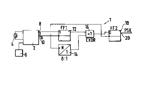
In Figure 1, a transmitting section 1 has a d~ita processor
2 whose clock is controlled by a quartz resonator 4. In
data source 6 of any type, data are generated which are fed
to the data processor 2. In the data processor: 2, the data
are converted into data coded in accordance w:~th the
Differential Manchester Code and emitted at a data
output 8. A clock signal is emitted from the processor 2 at
a clock output 10. The data from the data output a are re-
clocked in a first flip-flop 12 (FF1) to set them to a
precise time position. The processor clock from the clock
output 10 is divided, in the example in the ratio 8:1 (this
division ratio does not have any necessary relationship to
the standard representation of messages in thsa form of
bytes which each comprise a bits) by a clock divider 14.
The output signal of the first flip-flop 12 iaa fed to one
of the two inputs of an exclusive OR circuit :L6 (EXOR) and
the output signal of the clock divider 14 is :fed to the
other input of said~circuit 16. The exclusive OR circuit 16
emits an output signal having the value logic 1 only if
exactly one of its input signals has the value logic l;
this is symbolized by the symbol ~~=1~~ inside r_he circuit
symbol. The exclusive OR circuit 16 brings about an
CA 02279585 1999-08-03
4
inversion, controlled by the data output of the first flip-
flop 12, of the clock from the output of the clock divider
14, in each case during the passage of the clock through
zero. The output signal Of the exclusive OR circuit 16 is
phase-modulated with two phases which differ by 180° and
2pSK occurs. The output signal of the exclusiyre OR circuit
16 is fed to a second flip-flop 18 (FF2) in which switching
peaks, which are generated in real exclusive OR circuits,
axe eliminated. The signal appearing at the data output 20
of the second flip-flop 18 has been cleaned up in terms of
switching peaks and can be processed technically further,
in particular a phase-modulated signal which can be
transmitted via a data channel.
In the arrangement according to Figure 2, the received
phase-modulated signal to be demodulated is first fed to a
comparator 40 which generates precise pulses again having
constant amplitude from the phase-modulated signal which
may have been modified or rounded in the course of the
transmission. A clock-recovery device 42 recovers a clock
signal having a 1:1 duty factor~from the signal leaving the
comparator 40 at its output. The data signal ;leaving the
comparator 40 and the clock signal leaving the device 42
are fed to an exclusive OR circuit 44 at its two inputs and
said circuit brings about a demodulation of the phase-
modulated signal. The output of the exclusive OR circuit 44
is connected to the input of a low-pass filter 46 at whose
output the demodulated data signal, which corresponds to
the output signal at the output 8 of the processor 2 of
Figure 1 or is inverted with respect thereto, is available.
The clock signal at the output of the device 42 has the
clock frequency as it is available at the output of the
clock divider 14 of Wle ai'1'dilc~.etttCtll. auuc~tdi~a~' tv Figure 1.
In the detailed block circuit diagram of Figure 3, the
phase-modulated signal, which has to be demodulated, ie fed
to the input of a variable amplifier 60, whose gain can be
CA 02279585 1999-08-03
adjusted. The output 62 of the variable amplifier 60 is
connected via a low-pass filter 64 to the input of a
rectifier arrangement 66, at whose output a signal is
emitted which is proportional to the amplitude at the
5 output 62 of the variable amplifier 60. Said signal is fed
to a gain-controlled amplifier 68 at its first input 69 and
a reference voltage Uref is fed to a reference input 70 of
the gain-controlled amplifier 68. The output of the gain-
controlled amplifier 68 is connected to an adjustment input
of the variable amplifier 60 and alters its gain. In this
way, a control ie carried out which ensures that the output
signal of the rectifier arrangement 66 is exactly equal to
the reference voltage Uref. The output signal of the
variable amplifier 60 then has the amplitude necessary and
desired for the further processing.
Connected to the output of the low-pass filter 64 ie a
comparator 80 whose function, is comparable with that of the
comparator 40 in Figure 2. The data signal from the output
of the comparator 80 is fed to an input of an exclusive OR
circuit 84, to whose other input the clock signal necessary
for the demodulation is fed. Compared with the arrangement
according to Figure 2, this is recovered in a somewhat more
complicated way and, to be specific, the output signal of
the comparator 80 is first fed to an edge detector 88 which
detects the rising and falling edges. The output signal of
the edge detector 88 is fed to an input of a PLL circuit
90, which delivers an output signal having double the clock
frequency. In said output signal, gaps in the clock signal
are filled in. The edge detector 88 forms in each case a
pulse for each of the two edges (rising edge and falling
edge). A clock divider 92 reduces the frequen.~y of the
output signal of the PLL circuit 90 in the ratio 1:2 and
thereby generates the clock signal with the correct
frequency and 1:1 duty factor.
CA 02279585 1999-08-03
6
As also in the case of the arrangement according to Figure
2, the exclusive OR circuit 84 is followed by a low-pass
filter which carries here the reference symbol 94, and in
the arrangement according to Figure 3, the signal leaving
the low-pass filter 94 is furthermore clocked ao as to be
peak-free by a flip-flop 96 to whose clock input the clock
signal from the output of the clock divider 92 is fed.
Figure 3 furthermore shows that not only the abovementioned
to phase-modulated signal (PSK) is fed to the input of the
variable amplifier 60, but a useful signal, s~~mbolized by
the letters TV, which, in the example, is a signal in the
frequency range from 5 MHz to 70 MHz for the upstream
channel (cable phone), is fed to it simultaneously. said
signal is taken off at the output 62 of the variable
amplifier 60, optionally by a band-pass filter 100. The
variable amplifier 60 amplifies the useful signal TV in the
same way as the phase-modulated signal. In the exemplary
embodiment, the last-mentioned phase-modulated signal is
therefore a pilot tone which reveals the amplitude to which
it has to be amplified at the receiving end eo that the
useful signal also acquires the amplitude necessary for its
further use.
z~ Figure 4 shows the representation of the bite 0 and 1 in
accordance with the Differential Manchester Code. The bit 0
is notable for the fact that a transition is present in the
bit centre.~The bit 1 is notable for the fact that no
transition is present in the bit centre. Additionally,
transitions are present at the bit boundaries. As can
easily be seen, a phase reversal of the bit 0 ox the bit 1
does not bring about any interchange of the bits themselves
because the transition mentioned is also present in the
case of the bit 0 after phase inversion, but not in the
case of the bit 1. Other codings in which this property
described last exists can also be used for the invention,
CA 02279585 1999-08-03
7
As becomes clear from the above description of the
exemplary embodiment, the receiving device or demodulation
device according to the invention does not comprise any
devices for fixing a particular phase position for the
demodulated signal. The method according to the invention
therefore makes it possible to simplify the receiving-end
circuit compared with conventional phase-modulation methods
in which the phase position of the signal sent: has to be
~re-established.
to
The above description serves as an explanation and is not
intended to restrict the area of protection of the
invention. That the invention can also be applied in
modulation methods other than 2PSK is not ruled out.