Note: Descriptions are shown in the official language in which they were submitted.
CA 02279956 1999-08-OS
WO 98/36626 ~ PCT/US98/02707
-1-
PRINTED CIRCUIT ASSEMBLY
Backnround of the Invention
1. Field of the Invention
The present invention relates to the field of printed circuit assembly
construction. More specifically, the
present invention relates to component and lead soldering techniques for
preventing solder reflow during serially
performed soldering steps.
2. Description of the Related Technology
In the manufacture of electrical and electronic products, it is essentially
universal practice to create circuits
by soldering components to printed circuit boards which incorporate conductive
traces interconnecting the components
in the desired manner. In some instances, components are individually hand
soldered to their appropriate locations.
In other applications, several components are placed on a printed circuit
board at once, and are soldered in place
essentially simultaneously by a wave soldering method, or by an infrared or
convection oven reflow technique.
Reflow methods are especially common in printed circuit assemblies which
include surface mount components.
In a typical reflow procedure, the pads of the printed circuit board traces
are coated with a solder paste
by a stencil or screening process. Circuit components such as resistors,
capacitors, and the like are then secured
to their appropriate positions, typically with a small amount of adhesive. The
assembly is then placed inside an oven,
where the solder paste is raised to a temperature above its temperature of
"liquidus", the temperature at which the
solder is completely liquid. Upon cooling, the solder solidifies, securing the
components to the pads.
In many modern electronic applications, a printed circuit assembly as
described above is packaged or
encapsulated to form a single electronic module having terminals andlor leads
for external connection to other
circuitry. Such a module can be then used as a component of another,
"downstream", printed circuit assembly. In
this case, the terminals or leads of the module are soldered to another
printed circuit board at a downstream
manufacturing facility. This soldering process may again comprise hand, wave,
ar reflow soldering techniques. It
can be appreciated that during this subsequent soldering procedure performed
on the module, it is desirable to have
the solder interns! to the module remain below its temperature of "solidus",
the temperature at which the solder alloy
is entirely solid. If the solder internal to the module is raised above the
solidus temperature, migration and cracks
will begin to form, reducing the stability of the internal solder connections.
If the liquidus temperature is approached,
the solder internal to the module may reflew again, forming internal short
circuits and causing module failure.
Efforts to resolve this problem have focused on the use of a module solder
system which have higher
solidus and liquidus temperatures than the soldering system used to secure the
module to the other printed circuit
board. Most common solders use alloys of tin (Sn) and lead (Pb) having a
solidus temperature of approximately 183
degrees C. A 63% tin, 37% lead (63Sn137Pb) alloy is a common formulation, and
ratios can often range from 40%
to 60% Pb, with the balance being Sn. Although these tin-lead alloys are most
common, other elements can be
added or substituted for all or part of the Pb or Sn to produce solders with
different mechanical strengths, grain
sizes, or liquiduslsolidus temperatures. Such elements include, for example,
cadmium (Cd), bismuth (Bi), antimony
(Sb), and silver (Ag).
CA 02279956 1999-08-OS
WO 98/36626 ~ PCT/US98/02707
.2.
Most downstream printed circuit assembly manufacturers use a SnIPb alloy
solder at a reflow -oven
temperature of approximately 220 to 235 degrees C. To try to avoid module
reflow under these oven conditions,
a higher temperature module soldering system using an 85P6110Sb15Sn has been
employed in some commercially
available prior act modules. This solder has a solidus temperature of
approximately 239 degrees C, and a liquidus
temperature of approximately 243 degrees C. Even though modules using this
solder alloy have been produced using
pads plated first with nickel and then gold (thereby eliminating the thin
coating of SnIPb solder typically placed on
bare copper printed circuit board pads), these modules have been found to
exhibit undesired solder reflow and its
associated module failure in many downstream manufacturing environments which
use standard SnIPb solder alloys.
Another prior art system, one that is currently produced by the assignee of
the present application, uses
88Pb110SnJ2Ag solder on pads treated with a standard SnIPb solder dip rather
than nickel and gold plate. The
88Pb)10Sn12Ag solder alloy has a liquidus temperature of approximately 299
degrees C. This solder does not have
subsequent reflow problems in downstream manufacturing, but the initial reflow
temperature of 320 to 330 degrees
C required with this solder renders the use of expensive high temperature
printed circuit boards 30 such as
epoxylpolyphenylene oxide resin boards, available, for example, as type GETEK
(TM) from General Electric. This high
initial reflow temperature also tends to over-stress the components mounted on
the printed circuit board 30, as they
are commonly rated by component manufacturers to withstand only approximately
260 degrees C during soldering.
There is accordingly a need in the art far an improved module soldering system
which does not have reflow
problems during downstream incorporation into another printed circuit assembly
which utilizes standard PbISn
soldering methods. The module soldering technique should also use a reflow
temperature which can be tolerated by
standard inexpensive printed circuit boards and circuit components.
Summary of the Invention
In one aspect of the present invention, a lead-antimony alloy solder is
utilized which has liquidus and solidus
temperatures that avoid both subsequent reflow problems and component over-
stress. A printed circuit assembly
in accordance with this aspect of the invention thus comprises a printed
circuit board having a dielectric substrate
and conductive traces, and a circuit component secured to a pad on one of the
traces with solder, wherein the metal
content of the solder comprises approximately 90% lead and 10'Yo antimony. In
some embodiments, the pads
comprise a layer of copper having a layer of nickel and a layer of gold plated
thereon.
The present invention also comprises a method of making a printed circuit
assembly comprising the steps
of placing solder paste at selected locations on a printed circuit board,
placing circuit components on selected
locations on the printed circuit board, and reffowing the solder paste at a
temperature between approximately 280
degrees C and 290 degrees C. The method may advantageously include the use of
solder paste having a composition
of approximately 90% lead and 10% antimony.
Benefits in printed circuit assembly reliability created by the present
invention are especially apparent when
printed circuit assemblies in accordance with the principles described above
are incorporated into additional printed
CA 02279956 1999-08-OS
WO 98/36b26 PCT/US98/02707
-3-
circuit assemblies during subsequent manufacturing steps. Accordingly, the
present invention additionally comprises
a module which includes (1 ) a first printed circuit board comprising a
dielectric substrate and a plurality of conductive
traces, (2) a terminal having a portion coupled to one of the plurality of
conductive traces, and (3) a circuit
component secured to a pad on one of the traces with a first solder
composition which excludes tin. In addition, a
second printed circuit board comprising a dielectric substrate and a plurality
of conductive traces is provided, wherein
a portion of the terminal of the module is coupled to one of the plurality of
conductive traces on the second printed
circuit board with a second solder composition comprised of approximately 40%
or greater of tin. In preferred
embodiments of this assembly, reflow of the tin containing solder does not
affect the integrity of the non-tin
containing solder bonds of the module.
1p Brief Description of the Drawinns
FIG. 1 is a perspective view of a printed circuit assembly according to one
aspect of the present invention.
FIG. 2 is an internal perspective view of one sub-assembly which is part of
the printed circuit assembly of
FIG. 1.
FIG. 3 is a cross sectional view taken along lines 3-3 of FIG. 2 of a solder
bond in the module of that
Figure.
Detailed Description of the Preferred Embodiment
Preferred embodiments of the present invention will now be described with
reference to the
accompanying Figures, wherein like numerals refer to like elements throughout.
The terminology used in the
description presented herein is intended to be interpreted in its broadest
reasonable manner, even though it is being
utilized in conjunction with a detailed description of certain specific
preferred embodiments of the present invention.
This is further emphasized below with respect to some particular terms used
herein. Any terminology intended to
be interpreted by the reader in any restricted manner will be overtly and
specifically defined as such in this
specification.
In Figure 1, a portion of a printed circuit assembly 10 is illustrated. The
printed circuit assembly 10
comprises a printed circuit board 12 made of a dielectric material that may
comprise a wide variety of materials and
constructions well known to those of skill in the art. Some knowri
alternatives include laminated paperlphenolic and
glasslepoxy formulations. Copper traces 14 are provided on at least one
surface of the printed circuit board, and
are often also provided on the opposite side and on internal laminations of
the printed circuit board 12. The traces
14 provide conductive electrical connections between components mounted to the
printed circuit board 12 such as
the capacitor 16 and resistor 18 illustrated in Figure 1. Typically, the
components 16, 18 are soldered to the pads
22 of the traces 14, either with leads inserted into through-holes in the
printed circuit board 12 or an the circuit
board surface if the component is intended for surface mount.
In many printed circuit assembly applications, a packaged or encapsulated
module 20 forms part of the final
printed circuit assembly. Many different types of encapsulated modules are
presently available, including devices such
as optical isolators, amplifiers, digital logic circuits such as gate arrays
or processors and the like. In some cases,
the encapsulated module 20 will itself include an internal printed circuit
board with solder mounted components.
CA 02279956 1999-08-OS
- WO 98/36626 PCT/US98/02707
-4-
In communications applications, far example, it has become increasingly common
to encapsulate inductive components
such as telephone line interface transformers, high inductance common mode
chokes, two wire digital interface
transformers, and other similar components and circuits. Such components are
typically soldered to a printed circuit
board and encapsulated for subsequent incorporation into a "downstream"
printed circuit assembly as illustrated in
Figure 1. In these cases, the printed circuit board internal to the
encapsulated module 20 has its own traces which
connect to terminals 24 which may form leads out of the encapsulation. These
leads are then soldered to the
printed circuit board 12 in a manner similar to that described with respect to
the above-mentioned components such
as the resistor 16 and the capacitor 18. Of course, those of skill in the art
will appreciate that the type of circuitry
present in the module can vary, and the scope of the present invention is not
in any way limited to the nature of
the components or circuits provided in the encapsulation. As with the
components 16, 18, the encapsulated module
may be for through-hole mounting, or surface mount.
In some embodiments of the present invention, the components 16, 18, and the
encapsulated module 20
are soldered to the printed circuit board with a SnIPb alloy solder having a
solidus temperature of approximately 183
degrees C. As mentioned above, soldering of the printed circuit assembly 10
may be accomplished with hand
15 soldering, wave soldering, or with an IR or convection oven reflow
technique. The oven reflow methods are most
commonly performed when the printed circuit assembly 10 comprises a large
number of surface mount components.
During an oven reflow process with SnlPb solder having a solidus temperature
of 183 degrees C, the reflow oven
temperature is typically approximately 220 to 240 degrees C. This ensures that
all of the solder is raised above
the liquidus temperature so that sufficient wetting and intermetallic bonding
will occur.
20 Figure 2 illustrates the internal structure of an encapsulated module 20
according to one aspect of the
present invention. The module 20 comprises a printed circuit board 30 with
components such as inductors andlor
resistors 32 soldered to pads on traces 34 on the surface of the printed
circuit board 30. As a specific example,
illustrated also in Figure 3 and described in more detail below, a surface
mount resistor 38 is secured to a pad on
a trace by a solder bond 36. Internal construction of the module 20 may thus
be similar in many ways to the
downstream printed circuit assembly illustrated in Figure 1.
Due to size considerations, surface mount components are generally used for
many components in
encapsulated modules 20 of the type illustrated in Figure 2. Surface mount
components are generally bonded to the
printed wiring board by screening solder paste onto selected locations of the
printed circuit board and securing the
component to the board in appropriate relation to the screened on solder paste
via adhesive. The entire assembly
is then usually placed in a reflow oven to raise the solder above its liquidus
temperature. Lfpon cooling. the solder
bonds are formed. Non-surface mount components, like typical inductors, are
hand soldered to the printed circuit
board 30 following the oven reflow procedure.
After incorporation into the downstream printed circuit assembly 10, the
module 20 may again be placed
into a reflow oven. Accordingly, the solder system used to secure components
to the printed circuit board 30 inside
the encapsulated module 20 should withstand the temperature found in
subsequent soldering steps without bond
weakening through partial or total solder reflow within the module 20. Prior
art attempts to prevent this undesirable
CA 02279956 1999-08-OS
WO 98/36626 PCTNS98/02707
.5.
reflow in the module 20 have included significant drawbacks. Thus, a solder
formulation should have a sufficiently
high solidus temperature to remain solid in subsequent soldering procedures.
While it is true that many solder
formulations have solidus temperatures well above the typical 220 to 240
degree C used in downstream reflow
soldering operations, the liquidus temperature of the solder used in the
module 20 should also be low enough that
the necessary oven temperature used to perform the initial reflow process on
the module 20 does not damage either
the printed circuit board 30 or the components 32, 38. As mentioned above,
attempts at finding suitable soldering
systems which satisfy these needs have, prior to the present invention, been
unsuccessful as to one or the other
requirements.
An improved solder bonding system which avoids these disadvantages of the
prior art is illustrated in Figure
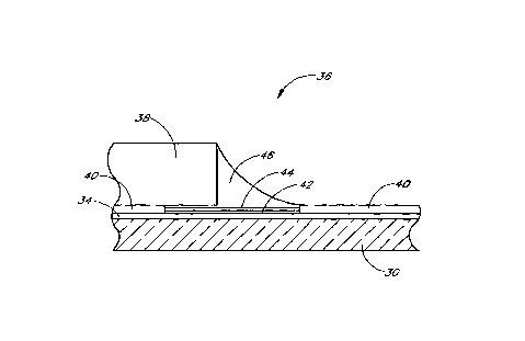
3, which shows a cross sectional view of one surface mount component 38 of
Figure 2 bonded to the printed circuit
board 30. Referring therefore to Figure 3, the printed circuit board 30
includes a trace 34, preferably of copper.
The trace thickness will vary with the required current capacity of the
connection, but a thickness of approximately
1.4 mil is suitable for many applications. Except at the pad region, the trace
34 is covered with a layer of solder
mask 40 which may suitably be approximately 1.5 to 2.0 mil thick. The
component 38 is secured to the printed
circuit board 30 to a pad on the trace with a suitable quantity of solder 46.
Preferably, the metal content of the
solder 46 is approximately 90% lead and 109'o antimony (90Pb110Sb). Generally,
the solder 46 is applied as a
quantity of solder paste having a mesh size of -200+325, a metal content of
92%, and comprising a water soluble
or RMA flux.
The 90Pb110Sb solder composition has a solidus temperature of approximately
252 degrees C, and a liquidus
temperature of approximately 260 degrees C. This solder composition thus has a
solidus temperature slightly higher
than the 220-240 degrees C typically encountered in subsequent downstream
incorporation into a second printed
circuit assembly. Furthermore, the liquidus temperature of the 90Pb110Sb
solder is at a temperature which
inexpensive printed circuit board 30 material and electrical components can
tolerate without significant harmful
effects.
It may be noted that initial experiments with 90Pb110Sb solder were not
particularly encouraging. In many
trial modules, reflow during downstream manufacturing processes recurred when
90Pb110Sb solder paste was
substituted for 88Pb110Sn12Ag solder paste. However, additional
experimentation revealed that the performance of
the 90Pb110Sb system improved significantly if the pads on the printed circuit
board were gold plated rather than
dipped in a PbISn solder bath to coat the pads. Accordingly, preferred
embodiments of the present invention provide
a pad comprising a portion of the trace 40 having a first layer of nickel 42
plated thereon. The nickel thickness
can vary widely, but is preferably between approximately 80 and 120 micro-
inches thick. On top of this nickel film
42, a gold plating is provided, preferably approximately 5 to 10 microinches
thick. During the reflow process, the
gold layer evaporates into the solder alloy, and a strong intermetallic bond
is formed with the nickel. Though the
solder bond is actually formed with the nickel layer, the gold is provided to
prevent nickel oxidation which occurs
rapidly when nickel is exposed to air, and which would interfere with solder
bond formation during the reflow
CA 02279956 1999-08-OS
- WO 98/3662b PCTNS98/02707
-6-
process. It can be appreciated that the layers illustrated in Figure 3 are not
drawn to scale for clarity, and are
shown much thicker than they would actually appear in visual inspection.
The substitution of a gold-solder alloy interface for an interface comprising
the 90PbllOSb alloy and the
PblSn coating often provided on bare circuit boards apparently stabilizes the
solid phase of the 90Pb110Sb alloy,
thereby raising the solidus temperature enough to prevent the initially
observed reflow problems. Furthermore, the
iiquidus temperature of the 90Pb110Sb alloy remains low enough that the
initial reflow step in the manufacture of
the module 20 does not over-stress standard printed circuit board materials or
circuit components such as resistors
and capacitors.
Manufacture of a preferred encapsulated module according to one aspect of the
present invention therefore
begins with plating pads on the printed circuit board with a nickel film 42
and a gold film 44 as described above.
Solder paste including a 90Pbl10Sb solder alloy is screened onto appropriate
locations on the printed circuit board.
Components are placed on the printed circuit board with the solder paste, and
the assembly is placed in an IR or
convection oven for reflow soldering of the components at a temperature of
approximately 280 to 290 degrees C.
This ensures that all of the solder shaving a liquidus temperature of
approximately 260 degrees C) is completely
molten and the appropriate surfaces are wetted with the solder alloy. After
cooling and bond formation, the printed
circuit board 30 is encapsulated to form the module 20.
Subsequent downstream manufacturing operations may then take place to
incorporate the module onto
another printed circuit board. In most common cases, a PbISn alloy solder
system will be used far this downstream
operation. The oven temperatures used in these downstream operations of
typically 220 to 240 degrees C, will not
raise the temperature of the solder in the module to above the solidus
temperature of approximately 252 degrees
C, thereby preventing migration or reflow of the module solder during the
downstream manufacturing process.
Accordingly, the invention described and claimed herein overcomes the
aforementioned problems in the art by
providing a solder system which avoids reflow in downstream manufacturing, but
which can be used with inexpensive
printed circuit board material and circuit components.
The foregoing description details certain preferred embodiments of the present
invention and describes the
best mode contemplated. It will be appreciated, however, that no matter how
detailed the foregoing appears in text,
the invention can be practiced in many ways. As is also stated above, it
should be noted that the use of particular
terminology when describing certain features or aspects of the present
invention should not be taken to imply that
the broadest reasonable meaning of such terminology is not intended, or that
the terminology is being re-defined
herein to be restricted to including any specific characteristics of the
features or aspects of the invention with which
that terminology is associated. The scope of the present invention should
therefore be construed in accordance with
the appended Claims and any equivalents thereof.