Note: Descriptions are shown in the official language in which they were submitted.
CA 02280385 1999-08-16
SC-5303-C
CONTROL ARRANGEMENT AND METHOD FOR HIGH-SPEED
SOURCE-TRANSFER SWITCHING SYSTEM
BACKGROUND OF THE INVENTION
1. Field of the Invention
The present invention relates generally to high-speed source-transfer
switching systems
and more particularly to a control arrangement and method that controls the
transfer of a load
from one source to another in a desirable fashion to minimize transfer delays
while also avoiding
undesirable current flow between the sources.
2. Description of Related Art
High-speed source-transfer switching systems (HSSTSS) for electrical power
distribution
systems provide reliable, continuous power delivery to a load by transferring
the supply of the
load from a first source to a second independent source when undesirable
characteristics are
sensed in the first source. To achieve high-speed transfer operation, one type
of HSSTSS utilizes
solid-state switches formed by thyristors, one solid-state switch for each of
the sources. These
high-speed switches are also known as static transfer switches. To control the
transfer
operations, the HSSTSS utilizes control arrangements to provide appropriate
control signals to
control the operation of the thyristors of each solid-state switch via the
gate of each thyristor.
The control arrangements sample the voltage waveforms of each source to detect
when transfer
between the sources is necessary, e.g. sensing outages and momentary
interruptions as well as
voltage sags and swells based on the source supplying the load being above or
below preset
levels. Under certain circuit conditions, transfer between sources by the
control arrangements
can introduce undesirable transfer delays and/or permit undesirable current
flow between the
sources. The arrangement in U.S. Patent No. 5,808,378 avoids undesirable
current flow between
sources by delaying transfer until a polarity comparison is satisfied that
ensures that the current
will flow in the incoming source after transfer will be in opposition to the
current flowing in the
outgoing source before transfer. Undesirable transfer delays are also
minimized by establishing a
forced commutation condition before transfer between sources, i.e. transfer is
delayed until the
CA 02280385 1999-08-16
SC-5303-C
incoming source voltage differential and the outgoing current establish an
initial change in
current flow in opposition to current flow in the switch to be turned off.
SUMMARY OF THE INVENTION
Accordingly, it is a principal object of the present invention to provide a
control
arrangement and method for high-speed source-transfer switching systems that
avoids
undesirable current flow via open-transition transfers to avoid the
paralleling of sources.
It is another object of the present invention to provide a control arrangement
and method
for high-speed source-transfer switching systems that minimizes undesirable
transfer delays by
establishing appropriate conditions before performing the transfer between
sources.
It is a further object of the present invention to provide a control
arrangement for solid-
state transfer switches that inhibits the transfer of a load from one source
to another if the transfer
condition is initiated by a downstream fault.
It is yet another object of the present invention to provide a control
arrangement for high-
speed source-transfer switching systems that both avoids undesirable current
flow between
sources via either the establishing of forced commutation conditions or by
waiting before issuing
control signals to perform the transfer between sources.
These and other objects of the present invention are efficiently achieved by
the provision
of a control arrangement and method for a power electronic system configured
as a high-speed
source-transfer switching systems (HSSTSS). The HSSTSS supplies an electrical
load with
alternating current from either a first source or a second source via
respective first and second
solid-state switches. The HSSTSS also includes a controller that samples the
voltage waveforms
of each of the first and second sources to detect when transfer between the
sources is desirable,
e.g. outages or voltage that is either too low or too high. The controller
provides appropriate
control signals to control operation of the solid-state switches and transfer
supply of the load
therebetween. The control arrangement avoids undesirable current flow between
sources via a
comparison of the voltages of the-sources and current in the outgoing source,
i.e. a polarity
comparison to ensure that the current that will flow in the incoming source
after transfer will be
in opposition to the current flowing in the outgoing source before transfer.
Thus, the transfer is
-2-
CA 02280385 1999-08-16
SC-5303-C
delayed until the polarity comparison is satisfied. Additionally, the control
arrangement
minimizes undesirable transfer delays by establishing appropriate transfer
conditions before
issuing control signals to perform the transfer between sources, i.e. the
transfer to turn on the
incoming switch is delayed until after appropriate conditions establish that
the outgoing source is
off or can be effectively turned off. One form of appropriate conditions
include the establishing
of forced commutation conditions, preferably established by the incoming
source voltage
differential and the outgoing current being of the same polarity such that the
voltage differential
across the solid-state switch that is being turned on is sufficient to
establish an initial change in
current flow in opposition to the current flow in the solid-state switch to be
turned off. The
lo appropriate forced commutation is established by the voltage differential
between the two
sources being of sufficient magnitude to force the outgoing current to zero.
Additionally, under
certain conditions, the transfer is accomplished by awaiting the next current
zero.
BRIEF DESCRIPTION OF THE DRAWING
The invention, both as to its organization and method of operation, together
with further
objects and advantages thereof, will best be understood by reference to the
specification taken in
conjunction with the accompanying drawing in which:
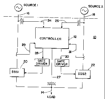
FIG. I is a one-line, block diagram representation of a power electronic
system
configured as a high-speed source-transfer switching system utilizing the
control arrangement of
the present invention;
FIG. 2 is a one-line, diagrammatic representation of portions of a solid-state
switch of
FIG. l;
FIG. 3 is a state diagram representation of a high-speed source-transfer
switching system
illustrating a specific control arrangement of the present invention;
FIGS. 4 and 5 are flow diagrams illustrating portions of the control
arrangement of FIG.
4;and
FIG. 6 is a one-line, block- diagram representation of another circuit
configuration
different than FIG. 1.
-3-
CA 02280385 1999-08-16
SC-5303-C
DETAILED DESCRIPTION
Referring now to FIG. 1, a high-speed source-transfer switching system
(HSSTSS) 10
includes a controller stage 12 to provide an illustrative embodiment of the
control arrangement
and method of the present invention. The HSSTSS 10 supplies a load at 14 with
an alternating-
current waveform via either a first AC source at 16 or a second AC source at
18. The first and
second AC sources 16 and 18 and the load at 14 as provided in an electrical
power distribution
system are typically multi-phase circuits which are represented in FIG. 1 by a
one-line diagram.
The HSSTSS 10 includes a first solid-state switch, SSS1, 20 and a second solid-
state switch,
SSS2, 22. The HSSTSS 10 via the controller stage 12 controls either SSSI to
supply the load at
14 via the first source 16 or controls SSS2 to supply the load at 14 via the
second source 18. The
solid-state switches SSS1 and SSS2 may also be referred to as power electronic
switches.
The controller stage 12 samples the voltage waveforms of each source 16, 18,
e.g. via
respective sensing inputs at 24, 26 to detect when transfer between the
sources is desirable, e.g.
sensing outages and momentary interruptions as well as voltage sags and swells
based on the
source supplying the load being above or below preset levels. The controller
stage 12 provides
appropriate control signals at 28, 30 to control the operation of each
respective solid-state switch,
SSS1 20 and SSS2 22. For example, assume that SSS1 20 is turned on by the
controller stage 12
via signals at 28 so as to be conductive and supply the load at 14. If the
controller stage 12 via
the sensing input 24 senses that the voltage of the first source at 16 is
exhibiting undesirable
characteristics, the controller stage 12 via the control signals at 28, 30
turns off SSSI and turns
on SSS2 so as to transfer the supply of the load at 14 from the first source
at 16 to the second
source at 18. As used herein, the term "incoming" is used to describe the
source and the SSS that
will be turned on to supply the load (e.g. the second source at 18 and SSS2 in
the illustrative
example), and the term "outgoing" is used to describe the source and the SSS
that is being turned
off (e.g. the first source at 16 and SSS 1 in the illustrative example).
Referring now to FIG. 2, each of the solid-state switches SSS 1 and SSS2
includes one or
more arrays of back-to-back connected thyristors, e.g. 40a and 40b for SSS 1
and 42a and 42b for
SSS2. In illustrative implementations, each array of thyristors is rated in
the range of 2-10kv. To
-4-
CA 02280385 1999-08-16
SC-5303-C
provide operation in medium voltage systems, e.g. operating in the range of 2-
34.5 kv, one or
more of such thyristors SSS1 and SSS2 are connected in series for each phase
of the sources, e.g.
a plurality of such thyristors being referred to as a stack. Thus, while the
term thyristor is used
for the solid-state switches SSS 1, 40 and SSS2, 42, this commonly refers to a
thyristor stack.
Considering now operation of the control arrangement and method of the present
invention, transfer of the load at 14 from one source to the other, e.g. the
first source at 16 to the
second source at 18, is generally accomplished by removing the gating signals
at 28a, 28b to shut
off SSSI and starting the gating signals at 30a, 30b to turn on SSS2. Thus,
the first source at 16
ceases to supply the load at 14 and the second source at 18 begins to supply
the load at 14. This
general approach can encounter problems especially when the transfer is
initiated due to an
upstream fault on the outgoing source, e.g. the first source at 16 in the
illustration. For example,
because power system loads generally are not of unity power factor, there are
times when the
current between the source and the load flows in opposition to the source
voltage, i.e. the polarity
of the voltage and current are different. If a fault and the initiation of a
transfer occur when the
current and voltage are of the same polarity, i.e. the current flows into the
load (defined as
positive) and the source voltage (relative to ground) is also positive, the
cessation of gate signals
to SSS1 quickly followed by the application of gate signals to SSS2 results in
a desirable transfer
referred to as forced commutation since the current from SSS2 opposes the
current flowing in
SSS1, rapidly driving the current in SSS1 to zero. However, if the load
current and the first
source voltage at 16 are of opposite polarity at the time transfer is
initiated, e.g. if the source
voltage at 16 is positive and the load current is negative, when the gating
signals from SSS 1 are
removed, the thyristor 40b will continue to conduct until the occurrence of a
current zero. If
SSS2 receives gating signals before the current zero in SSS 1, the second
source at 18 can supply
current but this current flow will not be in opposition to the current in SSS
1 which results in a
condition referred to as a shoot-through via the thyristors 42b and 40b. If
the first source at 16
has a fault condition, the second source at 18 would begin to feed this fault
condition which, of
course, is very undesirable. Thus-the present invention is arranged to provide
open-transition
transfers and not closed-forward transfers.
-5-
CA 02280385 1999-08-16
SC-5303-C
In accordance with important aspects of the present invention, the controller
12 performs
the transfer and the application of the appropriate gating signals based on a
polarity comparison
between the outgoing current and the differential voltage between the first
and second sources at
16, 18, e.g. by delaying the application of the gate signals to the incoming
thyristor 42b in the
illustrative example under predetermined detected conditions as explained in
more detail
hereinafter. Specifically, the source-voltage differential (i.e. difference),
the voltage across the
incoming SSS, is used to define a positive indication of the initial current
which will flow
through the incoming SSS. If the initial current which will flow through the
incoming SSS
opposes the current in the outgoing source, forced conunutation will occur and
no delay of the
1o application of the gate signals to the incoming SSS2 is necessary. On the
other hand, if the
initial current which will flow through the incoming SSS supports the current
in the outgoing
source, a shoot-through would occur, and a delay of the application of the
gate signals to the
thyristor 42b is performed, i.e. until the polarity comparison is satisfied.
The incoming source-
voltage differential may be determined by the load voltage at 14 as sensed via
a sensing input 27
or by the differential of the source voltages sensed at 24, 26. Additionally,
after a decision to
transfer occurs, the controller 12 is arranged to not immediately remove or
cease gate signals to
the outgoing SSS, e.g. SSS1. Instead, the controller 12, after a decision to
transfer is made, waits
until the occurrence of appropriate transfer conditions.
Considering now additional important aspects of the present invention and
referring now
additionally to FIG. 3, the depicted state diagram illustrates a specific
implementation of the
control of the high-speed source-transfer switching system to transfer between
sources. Each
phase of the each source traverses the state diagram of FIG. 3 independently.
A "First Source
On" state 150 depicts the condition of the system when the first source 16 is
supplying the load at
14 and a "Second Source On" state 152 depicts the condition of the system when
the second
source 18 is supplying the load at 14. Any decision to leave the states 150 or
152 is based on any
phase of the source being found to be unsuitable and the decision is then made
for all phases of
that source, assuming that the other available sources are determined to be of
better quality than
the present source.
-6-
CA 02280385 1999-08-16
SC-5303-C
For example, in an illustrative embodiment, if the controller 12 determines
that a severe
sag or swell is present on this first source 16, after the second source 18 is
verified to be suitable,
a transfer to the second source is begun with a transition to a "Forced
Commutation State" 154.
In a specific arrangement, the controller 12 also verifies that the sag
condition is not caused by a
downstream fault before proceeding. If the forced commutation conditions are
satisfied, a
transition is made to the "Second Source On" state 152 via the removing of the
gate signals from
SSS1 and applying gate signals to SSS2. Subsequently, if the controller 12
determines that a
severe sag or swell is present on the second source 18, after the first source
16 is verified to be
suitable, a transfer to the first source 16 is begun with a transition to a
"Forced Commutation
State" 156. If the forced commutation conditions are satisfied, a transition
is made to the "First
Source On" state 150 via the removing of the gate signals from SSS2 and
applying gate signals
to SSS 1. When in the state 150, if the controller 12 determines that a
transfer to another source
is suitable due to another category of conditions, e.g. a predetermined swell
conditions or a more
minor sag, a transition is made to an "Await Transfer Conditions" state 158.
When suitable
transfer conditions are met, a transition is made to a "Timing" state 160.
When a timing
condition is met, a transition is made to the state 152. Alternatively, in the
state 158 or 160, if
suitable forced commutation conditions are met, a transition is made, as
indicated, directly to the
state 152. Similarly, when predetermined swell conditions or more minor sag
conditions are
detected, transitions are made from the state 152 through states 162 and 164
to the state 150. In
accordance with a preferred embodiment, when transfer is desired for one or
more conditions,
either transfer may be initiated via both transition paths, 154, 156 or 158-
160 or 162-164, such
that transfer is accomplished by whichever occurs first.
Referring now additionally to FIG. 4, the flow diagram depicts an
implementation of the
forced commutation conditions to be established in the states 154 and 156 of
FIG. 3. In
accordance with important aspects of the present invention, the forced
commutation conditions
of the flow diagram of FIG. 4 utilize the polarity of the sources, the
direction of current flow, and
a determination that the voltage differential between sources is sufficient to
force the load current
to zero in a suitable time frame corresponding to the point on the existing
waveform. These
forced commutation conditions are utilized in response to a detected severe
sag condition, e.g.
-7-
CA 02280385 1999-08-16
SC-5303-C
caused by a fault condition, before a transfer is made between sources. The
forced commutation
conditions are required and/or desirable for the more severe sag and swell
conditions because it is
not desirable to wait for a current zero nor can the current zero necessarily
be accurately
predicted in some of these situations, e.g. severe sags.
For the transition conditions to be established in states 158-160 and 162-164,
one
implementation turns off the outgoing switch and establishes that the switch
is off via the voltage
across the outgoing switch, e.g. the outgoing voltage minus the load voltage
being greater than
3% of the nominal peak voltage over a suitable time period or number of
samples thus
establishing that the outgoing switch is off, although it should be understood
that lower voltages,
e.g. in excess of 100 volts should suffice. The transition conditions 158-160
and 162-164 are
utilized for the less severe category of disturbance conditions because forced
commutation
conditions are not necessarily required and can not always be satisfied in the
presence of such
conditions.
In FIG. 4, process flow begins in a block 170 which responds to a request for
transfer.
The process flow then proceeds to a determination block 172 to determine if
the transfer request
is for the more severe fault conditions, and if so, the process flow proceeds
in parallel to two
process blocks 174 and 176. If this is not a fault condition, the process flow
returns to the block
170. The process block 174 calculates source differentials and a parameter
denoted "DV" which
corresponds to the voltage differential between the sources multiplied by the
sign of the reference
voltage. This parameter DV is stored in a process block 178. The process block
176 calculates
the load current IL through the outgoing switch and supplies this to a
determination block 180,
which also receives as an input the stored DV parameter. The block 180
determines whether the
product of these two inputs is greater than zero, and if so, the process flow
proceeds to another
determination block 182. If the product is not greater than zero, the process
flow returns to the
block 170. The determination block 182 determines whether the ratio of "t"
(the time to perform
a transfer) to the time "to" (the time remaining before the next voltage zero)
is less than 1 so as to
establish that a transfer is possible. If the result is less than 1, the
process flow proceeds to a
process block 186 to stop the gating of the outgoing switch. The process flow
then proceeds to
-8-
CA 02280385 1999-08-16
SC-5303-C
the termination block 188 to start the incoming switch gating. If the
determinations in the block
182 is no, the process flow returns to the block 170.
This flow process can be summarized as performing the following relationship
of
conditions:
L i
tt < 1, ie when Lo 1 V< 1
o
V
O
where:
- Vo: the maximum, steady-state voltage difference between the reference
voltage and
the sag level 5 voltage
- io: the peak current flowing into the load. Note that it is not the rated
current of the
HSST unit
- to: based on the point on wave at which the transfer request is made, the
time
remaining before the reference voltage next goes through a zero
- Lo: total source inductance, e.g. approximately 0.6mH
and the properties of the system are:
- V: the instantaneous difference between the incoming and outgoing voltages
- i: the instantaneous value of the load current
- t: the time required to make a transfer. This value is actually calculated,
since we
know that if the dimensionless time (t/to) exceeds one, then a loop current
will result
- L: the value of the line inductance between the outgoing switch and the
nearest
significant voltage source. Where there are large lumped capacitors on the
system,
this will be the inductance up to the nearest pole-top bank, but where there
are none,
then it will be the short circuit inductance of the line.
Of course, the value of Lo can be varied depending on system properties.
-9-
CA 02280385 1999-08-16
SC-5303-C
In accordance with a specific embodiment to provide a practical generalized
approach to
a correlation equation derived from commutation data and adjusted to provide a
conservative
approach to ensure proper commutation, the following relationship is utilized
for the process
block 182:
OV = p=i4, where p= 26.5 and q= 1.75.
This approach, being conservative, delays transfers which might be feasible in
borderline
conditions such that transfer will occur when the correlating equation is
later satisfied, e.g. with a
delay probably less than 3 milliseconds.
In accordance with additional aspects of the present invention to provide a
more
conservative approach to establish that the forced commutation conditions will
be satisfied for
possible borderline conditions and severe operating environments, a minimum
voltage criterion
is also utilized to ensure that the outgoing switch will remain off after the
incoming switch is
turned on. For example, a voltage in the range of 3% of the nominal peak
voltage over a suitable
time period or number of samples thus establishing that the outgoing switch is
off, although it
should be understood that lower voltages, e.g. in excess of 100 volts, should
suffice.
Referring now to FIG. 5 and in accordance with other important aspects of the
present
invention relating to an illustrative alternate embodiment to establish the
transfer conditions of
the "Current Zero" states 160 and 164, the process begins at a block 190 to
respond to a request
for transfer. If there is a request for transfer, the process flow proceeds to
a determination block
192 to determine if the transfer request applies to the current zero
conditions. If so, the process
flow proceeds through two process blocks 194 and 198 and a determination block
200 to
calculate the necessary parameters to evaluate if the rate of change in
current is less than zero in
the block 200. If the rate of change is satisfied, the process flow proceeds
to a determination
block 202 if a current zero is predicted. If a current zero is predicted, the
process flow proceeds
to a process block 204 to stop the gating of the outgoing switch (if not
already accomplished) and
start a delay timing interval. The process flow then proceeds to a termination
block 206 to start
the gating of the incoming switch. If the result in either of the
determination blocks 200 or 202
is not established, the process flow returns to the process block 194. In
blocks 198, 200 and 202,
T2/T1 is in the range of 2-5, with T1 in a specific implementation being about
.5 milliseconds, k
-10-
CA 02280385 1999-08-16
SC-5303-C
is approximately 50% in a specific implementation, IL is an instantaneous
overcurrent threshold,
and m is a maximum current level for the current zero prediction to be valid,
e.g. .16 per unit
with a rate of change dependency in a specific implementation, Di is the slope
of the current.
Referring now additionally to FIG. 6 and considering another illustrative
source transfer
switching system 110 where more than two solid-state switches are controlled,
a controller 112
of a high-speed source-transfer switching system (HSSTSS) 110 controls solid-
state switches
SSS1, 120, SSS2, 122 and SSS3 121 via respective control signal paths 128,
130, and 132. The
specific illustrative circuit configuration of FIG. 6 implements a split-bus
primary selective
system, which is used to split the load during normal operation. Specifically,
in normal
operation, a first source 16 supplies a first load circuit 114 via SSS 1 and a
second source 18
supplies a second load circuit 116 via SSS2, with SSS3 normally being turned
off
(nonconducting) and functioning as a bus-tie switch. Thus, each of the sources
16, 18 is a
preferred source for its respective load circuit 114, 116 and each is an
alternate source for the
other load circuit, 116, 114 respectively. When one of the sources at 16, 18
is lost or exhibits
undesirable characteristics, the controller 112, after a transfer decision is
made, and as described
hereinbefore, removes the signals at 128 or 130 and applies signals at 132
such that the load
circuits 114, 116 are supplied from one of the sources at 16 or 18. For
example, if the source 16
is lost, SSS1, 120wil1 be turned off and SSS3, 121, the bus-tie switch, will
be turned on to supply
the load circuit 114 while SSS2, 122 continues to supply the load circuit 116.
The polarity
comparison to establish the appropriate application of control signals in the
circuit configuration
of FIG. 6 utilizes the differential voltage across the incoming switch, e.g.
SSS3, 121 when
transferring the load circuit 114 so as to be supplied from the source 18 via
SSS3, 121 and SSS2,
122. Similarly, upon the return of the source 16, when the normal
configuration is to be restored,
the differential voltage across the incoming switch, e.g. SSS 1, 120 is
utilized for the polarity
comparison.
While there have been illustrated and described various embodiments of the
present
invention, it will be apparent that-various changes and modifications will
occur to those skilled in
the art. Accordingly, it is intended in the appended claims to cover all such
changes and
modifications that fall within the true spirit and scope of the present
invention.
-11-