Note: Descriptions are shown in the official language in which they were submitted.
CA 02280619 2004-05-20
ELECTRIC SHOCK PREVENTION APPARATUS
FOR USE WITH A COMPONENT HAVING
AN UNINSULATED EXTERIOR SURFACE
BACKGROUND OF THE INVENTION
Field of the Invention:
The present invention relates to an apparatus and method for preventing
electrical
shock due to contact with an uninsulated electronic component, such as a
passive infrared
detector. More particularly, the present invention relates to a mechanical
apparatus, such as a
finger guard, which restricts physical contact with an uninsulated component,
such as
infrared detector, carrying a voltage, and an electrical apparatus, such as a
current limiting
circuit, which limits current supplied to the uninsulated, to prevent
electrical shock due to
inadvertent or intentional contact with the uninsulated component.
CA 02280619 2006-09-11
-2-
Description of the Related Art:
A motion sensor switch, such as Model AT277W motion sensor switch
manufactured by Hubbell Incorporated, Orange CT, includes a passive infrared
detector (PIR), and an ambient light detector. Motion sensor switch can be
used, for
example, as an occupancy detector which shuts off lights after a delay in a
room when
no one is present in the room, and turns on the lights in the room when a
person
enters the room. Motion sensor switch also can be used, for example, as a
motion
sensor for an alarm system.
The motion sensor senses motion in an occupied area, such as an office,
conference
room in a building, or a home, and in turn controls the lighting loads to save
energy. The
motion sensor detects a change in the infrared energy radiating from the
occupant as the
occupant move in and out of or between the PIR lenses sensing lobes. The PIR
detector has
a pass band in the 8-14 m infrared range.
If a person enters the monitored area, the person changes the amount of
infrared
energy being detected by the PIR detector. Therefore, the magnitude of the
signal output by
PIR detector, which is representative of the amount of detected infrared
energy, will change.
The detection circuit in the motion detector device processes this signal, and
outputs a signal
indicating that the amount of infrared energy received by the infrared
detector has changed.
The control circuit interprets the signal output by the IR detection circuit,
along with
the signal provided by ambient light detector. If the signal provided by
ambient light
detector indicates that the ambient light in the monitored area is low (e.g.,
very little natural
light is present in the monitored area), the control circuit will turn on or
increase the
brightness of the lights in the monitored area. However, if the signal
provided by ambient
light detector indicates that the ambient light in the monitored area is
sufficient (e.g., due to
sunlight, etc.), the control circuit may not tum on or brighten the lights, or
may only brighten
the lights slightly. In either event, control of the lights is based on the
signals provided by
the infrared detector and ambient light detector.
If a person (occupant) then leaves the monitored area for a period of time
exceeding
the "off delay", the circuit of the motion sensor turns off the lighting load
in the monitored
area
The infrared detector and ambient light detector employed in a motion detector
switch of the type described above are non-insulated electronic components
which during
CA 02280619 1999-08-23
-3-
operation typically carry voltages on at least a portion of their outer
casing, or on exposed
uninsulated temlinals. Because these voltages can create an electrical shock
hazard, UL
Standards covering uninsulated live parts (i.e., UL773A, effective August 30,
1998) require
either that physical access to the infrared detector and ambient light
detector be restricted, or
s that the current provided to infirared detector and ambient light detector
be limited to less
than 500 A.
Accordingly, in a motion sensor switch of the type described above, a fresnel
lens,
which is made of, for example, polyethylene, flexible plastic or any other
suitable material, is
installed in front of infrared detector and ambient light detector. The lens
is most
1.o transmissive in the 8-14 m infi-ared range, but will also allow visible
ambient light (400-
700nm wavelength) to pass. This enables the infrared'detector and ambient
light detector to
receive infrared energy and ambient light, respectively, while also preventing
physical
contact with the infrared detector and ambient light detector.
Although a lens of the type described above is typically suitable for
preventing
15 contact with the infrared detector in the motion detector switch while in
place, tampering
(e.g., cutting, prying with a tool) with the motion detector switch may result
in the lens being
removed. Once the lens has been removed, the surfaces of the infrared detector
and ambient
light detector are exposed and can be contacted by, for example, a person's
finger, which
could result in the person receiving an electrical shock from the voltage and
current being
20 carried by those detectors. Furthermore, the lens is made of a material
which will usually
melt when exposed to fire. Therefore, due to the required infrared
transmicsive properties,
the lens is not capable of passing a 5-inch flame test required in UL773A.
Although it is possible to provide a flame resistant lens over the infrared
energy and
ambient light detectors, these type of lenses can be very expensive, and thus
not provide a
25 cost effective solution.
Accordingly, a continuing need exist for an apparatus and method which
provides
added safety in preventing electrical shock due to contact with infrared and
ambient light
detectors in, for example, a motion detector switch, which does not
significantly obstruct the
passage of infrared energy and ambient light to the infrared and ambient light
detectors,
30 respectively, and which also fully complies with UL773A.
CA 02280619 2004-05-20
-4-
SUMMARY OF THE INVENTION
Accordingly, the present invention seeks to provide an apparatus which
restricts
physical access to an uninsulated component, such as an infrared or ambient
light detector,
in a device, such as a motion detector device, to thus prevent electrical
shock due to the
voltage and current carried by the uninsulated component, and which fuliy
complies with
UL773A.
Another aspect of the present invention seeks to provide an apparatus which
restricts
physical contact with an uninsulated component, such as an infrared or ambient
light detector,
in a device, such as a motion detector device, while allowing a sufficient
amount of infrared
energy and light to be received by the uninsulated component to enable the
uninsulated
component to operate as intended.
A further aspect of the present invention seeks to provide an apparatus, such
as an
electronic circuit, which limits an amount of current provided to an
uninsulated component,
such as infrared or ambient light detector, in a device, such as a motion
detector device to
safeguard against electrical shock to a person contacting the uninsulated
component, while
enabling the uninsulated component to operate as intended.
These and other aspects of the present invention are essentially attained by
providing
an apparatus, such as a finger guard, for use with an electronic device, for
restricting physical
access to a component of the electronic device having a surface adapted to
carry a voltage.
The apparatus includes a housing which defines a first opening therein, and
which is adapted
to mount to the electronic device so that the first opening permits passage of
light to the
component. The apparatus further includes a projection arrangement, extending
from the
housing and defining a second opening which permits infrared energy and light
passing
therethrough to pass through the first opening to the component, while also
limiting physical
access to the surface of the component through the first opening.
The projection arrangement can include a plurality of projection which are
disposed
at intervals about the first opening, and which each include a first
projection portion which
extends away from the housing and a second projection portion which extends
transversely
CA 02280619 2006-09-11
- 4a -
of the extension direction of the first projection portion. The edges of the
second projection
portion of each projection falls substantially within a periphery defining the
second opening.
The above aspect, along with other aspects, are also essentially achieved by
providing
an apparatus, for use with an electronic device, for limiting current being
provided to an
s uninsulated component, such as a infrared detector of the electronic device,
from a circuit of
the electronic device. The apparatus includes a resistive element which
couples a terminal of
the uninsulated component to ground, and a capacitive element which also
couples the
terminal of the uninsulated component to ground. The resistive and capacitive
elements have
resistance and capacitance values, respectively, which limit the current to
less than about
1 o 500 A. The capacitive element preferably comprises a plurality of
capacitors which are
coupled in series. Therefore, if one of the capacitors becomes short-
circuited, the remaining
capacitor or capacitors provide a capacitive sufficient to enable the
apparatus to limit the
current being provided to the uninsulated component to less than about 500 A.
A method or restricting physical access to a spectral energy detector of an
electronic
15 device having an uninsulated external surface adapted to carry a voltage,
comprising the steps
of: providing a housing defining a first opening therein and a projection
arrangement
extending from the housing and defining a second opening therein; and
positioning the
housing in the electronic device such that the first opening is substantially
aligned with the
detector, the projection arrangement permitting spectral energy passing
through the second
20 opening to pass through the first opening to the detector while limiting
physical access to the
surface of the detector through the first opening.
A method for limiting a current being provided to a spectral energy detector
of an
electronic device from a circuit of the electronic device, comprising the
steps of: coupling
a current limiting circuit, comprising a resistive element and a capacitive
element coupled in
25 parallel, between a terminal of the spectral energy detector and ground;
and operating the
current limiting circuit to limit the current to less than about 500 A.
CA 02280619 2004-05-20
'5-
Other aspects, advantages and salient features of the invention will become
more
apparent from the following detailed description, which taken in conjunction
with the annexed
drawings, discloses preferred embodiments of the invention.
BRIEF DESCRIPTION OF THE DRAWINGS
Referring now to the attached drawings which form a part of the original
disclosure:
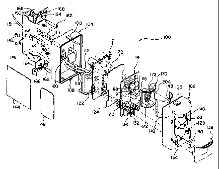
Fig. 1 is an exploded perspective view of a motion detector device employing a
finger guard according to an embodiment of the present invention;
Fig. 2 is an enlarged front view of the motion detector device shown in Fig.
1, with
the lens being removed to expose the finger guard;
Fig. 3 is an enlarged prospective view of the finger guard show in Figs. 1 and
2;
Fig. 4 is a front view of the finger guard shown in Figs. 1-3;
Fig. 5 is a cross-sectional view of the finger guard taken along lines 5-5 in
Fig. 4;
Fig. 6 is a cross-section view of the finger guard taken along lines 6-6 in
Fig. 4;
Fig. 7 is a cross-sectional view of the finger guard taken along lines 7-7 in
Fig, 4;
Fig. 8 is a top view of the finger guard shown in Fig. 4;
CA 02280619 2006-09-11
-6-
Fig. 9 is an enlarged detail view of the opening and projections of the finger
guard
shown in Fig. 4;
Fig. 10 is a schematic front view of an articulate probe according to UL
guidelines
UL773A, which is used to determine whether the finger guard shown in Fig. 4
sufficiently
limits access to the infrared detector and ambient light detector of the
motion sensor device
shown in Figs. 1 and 2;
Fig. 11 is a side view of the probe shown in Fig. 10;
Fig. 12 is a plan view of the proximal end of the probe taken in the direction
of lines
12-12 in Fig. .10;
Fig. 13 is a cross-sectional view of the probe taken along lines 13-13 in Fig.
10;
Fig. 14 shows a cross-sectional view of the finger guard shown in Figs. 3-9 in
relation to the distal end of articulate probe shown in Figs. 10-13;
Fig. 15 is a perspective view of a finger guard according to another
embodiment of
the present invention;
Fig. 16 is a top plan view of the fiinger guard shown in Fig. 15;
Fig. 17 is a top plan view of a finger guard according to a further embodiment
of the
present invention; and
Fig. 18 is an electronic schematic of a circuit according to an embodiment of
the
present invention for limiting current being provided to an infirared detector
in the motion
detector device shown in Figs. 1 and 2.
DETAILED DESCRIPTION OF THE PREFERRED EMBODIMENTS
A motion detector 100, in which a finger guard according to an embodi-
ment of the present inventon is employed, is illustrated in Figs. I and 2.
Motion
detector 100 can be, for example, model AT277W motion detector switch manufac-
ture by Hubbell Incorporated, Orange CT, or any other suitable motion
detector.
Motion detector 100 includes a front housing 102 and a rear housing 104, which
are
each made of a plastic, composite, or any other suitable material, and
interlock with each
other to form the housing of motion detector 100. Specifically, front housing
102 includes
latch members 106 on its top and bottom which receive locking tabs 108 on the
top and
CA 02280619 1999-08-23
-7-
bottom of rear housing 104 to releasable lock the front and rear housings 102
and 104
together.
Motion detector 100 further includes a circuit assembly comprising a power
supply
circuit board 110 having a wire 112 coupled thereto which connects to an AC
power source
(not shown) to provide power to the power supply circuit 110. Power supply
circuit board
110 also has a wire 113 coupled thereto which is used to provide an output of
the motion
detector 100 to, for example, control a lighting circuit.
Motion detector 100 further includes a printed circuit board assembly 114
including
components, such as motion indicator LED 116, infrared detector 118, and
ambient light
detector 119, the purposes of which are described in more detail below.
Circuit board
assembly 114 further includes connectors 120 which plug into the PCB 122 of
power supply
circuit board 110 to enable circuit board assembly 114 to receive power from
power supply
circuit board 110. An insulator 124 is positioned between power supply circuit
110 and
circuit board assembly 114 to prevent unintentional contact between components
on power
supply circuit board 110 and circuit board assembly 114.
Motion detector 100 also includes a light pipe 126 which is positioned over
LED 116
to direct light from LED 116 through an opening 128 in front housing 102. A
button 130 is
positioned on the front of front housing 102, and is mechanically connected to
override push
button 132 on circuit board assembly 114. Front housing 102 further includes a
switch
opening 134 which provides access to off/auto switch 136 on circuit board
assembly 114. A
door 138 is removably attached to front housing 102 to cover off/auto
switch'136, and thus
permits access to off/auto switch 136 only when removed.
Front housing 102 also includes a window 140 therein, which allows passage of
infrared energy and light to infrared detector 118 and ambient light detector
119, as is
described in more detail below. A lens 142, which is made, for example, of a
flexible plastic
material and is essentially transparent to infrared energy and usable for
ambient visible light,
is mounted in window 140. When lens 142 is mounted in window 140, lens 142
prevents
physical access to components, such as infrared detector 118 and ambient light
detector 119,
on circuit board assembly 114. Lens 142 includes tabs 143, the purpose of
which is
described below.
CA 02280619 1999-08-23
-8-
Motion detector 110 can also include a label 144, which is attached to wires
112 and
113, for example, and includes information pertaining to the wiring
attachment. Motion
detector 110 can further include a label 146, which is attached to external
portions of front
and rear housings 102 and 104, and includes information, such part number, UL
rating
criteria, and the like.
Motion detector 100 also includes a bracket assembly 148 having openings 150
therein, which receive locking tabs 108 of rear housing 104 and latch members
106 of front
housing 102, to mount bracket assembly 148 to the assembled front and rear
housings 102
and 104. Bracket assembly 148 further includes a ground wire 151, which can be
coupled to
ground or, for example, to a grounded terminal of power supply (not shown)
which provides
power to power supply circuit board 110 as described'above. A metal pin
assembly 152 is
mounted to bracket assembly 148 by a screw 154, whose shaft passes through
opening 156
in bracket assembly 148 and into opening 158 in pin assembly 152. Pin assembly
152 passes
through opening 160 in rear housing 104, and engages with a slot (not shown)
in power
supply circuit board 110 to provide an electrical connection between power
supply circuit
board 110 and ground wire 151.
Bracket assembly 148 further includes screws 162 which pass through openings
164
in bracket assembly 148 to mount bracket assembly and hence, motion detector
100, in an
electrical box, for example. Washers 166 can be used in conjunction with
screws 162 to
mount the bracket to the electrical box. Bracket assembly 148 also includes
additional
openings 168, which can receive additional screws, rivets, or any other
suitable structure to
motion detector 100 to the support surface.
As described above, a finger guard 170 according to an embodiment of the
present
invention is employed motion detector 100 as shown. Finger guard 170 is an
integral, one-
piece unit made, for example, of a hard or relatively hard plastic or
composite material, or
any other suitable material as required by UL773A Standards cited above.
Finger guard 170
also can include warning labels 172, which provide information pertaining to a
potential
hazard created by infirared detector 118 and ambient light detector 119 as
described in more
detail below.
As shown in Fig. 2, in particular, finger guard 170 is positioned between
circuit
board assembly 114 and front housing 102, so that finger guard 170 aligns with
or essentially
CA 02280619 1999-08-23
-9-
aligns with window 140 in front housing 102. When lens 142 is mounted in
window 140,
lens 142 covers the front of finger guard 170. For illustrative purposes,
however, Fig. 2
shows the motion detector 100 with lens 142 being removed to expose finger
guard 170.
As further shown in Fig. 2, and as described in more detail below, finger
guard 170
includes a circular or substantially circular opening 174 which aligns with
infrared detector
118 when finger guard 170 is mounted in motion detector 100. Finger guard 170
also
includes a substantially rectangular shaped opening 175 which aligns with
ambient light
detector 119 when finger guard 170 is mounted in motion detector 100. Hence,
as described
in more detail below, infrared energy and ambient light entering window 140 of
front
housing 102 passes through openings 174 and 175 in finger guard 170 and are
detected by
infrared detector 118 and ambient light detector 119, respectively.
Finger guard 170 is shown in more detail in Figs. 3-9. Finger guard 170
includes a
vertical wall portion 176, a top wall portion 178 and a bottom wall portion
180 which are
integral with each other. Vertical wall portion 176 has a planar or
substantially planar
portions 182 and 183, slanted portions 184 and 186, and a recessed planar or
substantially
planar portion 188 which extends parallel or substantially parallel to planar
portions 182 and
183. Planar portions 182 and 183 each has a thickness T1 of about 0.025
inches. Slanted
portions 184 and 186 each extend at an angle 01 with respect to their
respective planar
portion 182 and 183, respectively, and each has a width D1 measured from a
central vertical
plane Y which, as shown in Fig. 6, extends through the center of finger guard
170. In this
example, 01 is about 20 , and width Wl is about 0.320 inches. The combined
width W2 of
slanted portions 184 and 186 in this example is therefore about 0.640 inches.
Recessed planar portion 188 is divided by vertical plane Y into two halves
having
essentially equal widths, with the overall width W3 of recessed planar portion
188 in this
example being about 0.400 inches. The rear surface of recessed planar portion
188 is
recessed at a distance Dl from the rear surfaces of planar portions 182 and
183. In this
example, distance D 1 is about 0.044 inches.
A raised portion 189 extends outward from slanted portions 184 and 186 and
recessed planar portion 188. Raised portion 189 includes a circular or
substantially circular
portion 190 which encircles opening 174 in finger guard 170, and a
substantially rectangular-
shaped portion 191 which encircles second opening 175 in finger guard 170. In
this
CA 02280619 1999-08-23
-10-
example, circular portion 190 has a diameter of about 0.530 inches, and
opening 174 has a
diameter of about 0.400 inches, which is sufficient to accommodate infrared
detector 118
such that none of circular portion 190 obstructs the front surface of infrared
detector 118.
Circular portion 190 therefore has a thickness of about 0.130 inches. Also in
this example,
opening 175 has a length L1 of about 0.215 inches, with each lengthwise edge
of
rectangular-shaped portion 191 having about a 5 draft (see Fig. 9, in
particular), and has a
height H1 of about 0.160 inches with each heightwise edge of rectangular-
shaped portion
191 having about a 5 draft. In this example, rectangular-shaped portion 191
has a thickness
of about 0.030 inches, with each of the four corners of rectangular-shaped
portion 191 being
rounded to have an inner radius of about 0.030 inches.
Finger guard 170 further includes projection portions 192, 194, 196 and 198
which
each extend outwardly from raised portion 190 to a distance D2 from the rear
surface of
recessed planar portion 188, a distance D3 from the rear surfaces of planar
portions 182 and
183, and at an angle of about 2 with respect to vertical plane Y. In this
example, distance
D2 is about 0.215 inches, and distance D3 is about 0.171 inches. Further
details of
projection portions 192, 194, 196 and 198, and their purpose, are described
below.
Vertical wall portion 170 further includes vertical edge portions 200 and 202
which
extend outward from opposite side edges of planar portions 182 and 183,
respectively, in a
direction normal or substantially normal to planar portions 182 and 183 at a
distance D4
from the rear surface of planar portions 182 and 183, respectively. In this
example, distance
D4 is about 0.090 inches. The width W4 of finger guard 170 taken between the
inner
surfaces of vertical edge portions 200 and 202 is about 1.030 inches in this
example.
Vertical edge portion 202 includes a notch 204 therein having a depth D5 and a
length L2, which functions as a locating notch to position finger guard 170
correctly with
respect to lens 142 of motion detector 100. In this example, depth D5 is about
0.045 inches
and length L2 is about 0.120 inches. As shown in Fig. 1, notch 204 receives
tab 143 of lens
142 and thus maintains finger guard 170 at a predetermined position with
regard to lens 142.
Top portion 178 of finger guard 170 includes a lower planar or substantially
planar
portion 206, and an upper planar or substantially planar portion 208 which is
parallel or
substantially parallel to lower planar portion 206. Top portion 178 further
includes a step-
edge portion 212 which include an outer edge surface 214, a step surface 216,
and an inner
CA 02280619 1999-08-23
-11-
edge surface 218. Step edge portion 212 receives a ridge (not shown) along the
top inner
surface of lens 142 to assist in securing finger guard 170 to the lens 142
during assembly.
Outer edge surface 214 extends normal or substantially normal to lower planar
portion 206 and is integral with step surface 216 which extends normal or
substantially
normal to outer edge surface 214 and thus parallel or substantially parallel
to lower planar
portion 206 and upper planar portion 208. Inner edge surface 218 extends
between an edge
of upper planar portion 208 and an edge of steps surface 216 normal or
substantially normal
to step surface 216 and upper planar portion 208.
In this example, outer edge surface 214 extends for a height H2 which, in this
1 o example, is about 0.030 inches, and inner edge surface 218 extends for a
height H3 which, in
this example, is about 0.030 inches. Accordingly,. the overall height H4
between lower
planar portion 206 and upper planar portion 208 is about 0.060 inches in this
example.
Furthermore, as shown in Fig. 8, in particular, outer edge surface 214 extends
arcuately at a radius Rl which, in this example, is about 0.565 inches, and
inner edge surface
218 extends arcuately at a radius R2 which, in this example, is about 0.531.
Accordingly,
lower planar portion 206 and upper planar portion 208 each have a semi-
circular or
substantially semi-circular shape.
However, as further shown in Fig. 8, outer edge surface 214 includes straight
or
substantially straight portions 220 and 222, and inner edge surface 218
includes straight or
substantially straight portions 224 and 226. Straight portions 220-226 each
extend normal or
substantially normal to vertical wall portion 176 at a distance D6 from the
rear surface of
planar portions 182 and 183. In this example, D6 is about 0.130 inches.
Finger guard 170 therefore has an overall width W5 of about 1.080 in this
example as
measured between the outer surfaces of straight portions 220 and 222. Width W6
measured
between inner surfaces of straight portions 220 and 222 is about 1.010 in this
example.
Top portion 178 further includes projections 228 and 230 which each extend
from
upper planar portion 208 in a direction normal or substantially normal to
upper planar
portion 208 to a height H5 which is about 0.030 inches in this example.
Projection 228 has a
chamfered end 232, and projection 230 has a chamfered end 234. Chamfered ends
232 and
234 each extend at an angle of about 30 with respect to upper planar portion
208 and thus, at
an angle of about 30 with respect to the top surfaces of projections 228 and
230.
CA 02280619 1999-08-23
-12-
Projections 228 and 230 each extend backward along upper planar portion 208
from inner
edge surface 218 to a distance D7 from the back surface of respective planar
portions 182
and 183. In this example, distance D7 is about 0.250 inches.
Projections 228 and 230 each have a width W7 which, in this example, is about
0.050
inches. Outer sides of projections 228 and 230 each extend at an angle 02 of
about 5 with
reference to respective planes which are parallel to vertical plane Y. The
centers of
projections 228 and 230 are spaced at a width W8 which, in this example, is
about 0.750
inches, and are thus each at a distance W9 of about 0.375 inches from vertical
plane Y.
Top portion 178 further includes a slanted portion 236 which extends at an
angle 03
with respect to upper planar portion 208. In this example, 03 is an angle of
about 26 .
Vertical sections 238 and 240 extend downward in a direction normal or
substantially normal
to lower planar portion 206 to slanted portion 236 as shown. As further
illustrated, label 172
is attached to the inner surface of slanted portion 236. Slanted portion 236
has a width W10
which, in this example, is about 0.393 inches, and extends from the rear
surfaces of planar
portions 182 and 183 for a distance D8 which, in this example, is about 0.400
inches taken
along vertical plane Y. As further shown, the width Wl l of rear surface of
recessed planar
portion 188 is about 0.450 in this example, which is slightly greater than the
width W10 of
slanted portion 236.
Bottom portion 180 includes a lower planar portion 242 and an upper planar
portion
244 which extends parallel or substantially parallel to lower planar portion
242. Bottom
portion 180 further includes a step-edge portion 246 which includes an inner
edge surface
248, a step surface 250, and an outer edge surface 252. Step-edge portion 246
receives a
ledge (not shown) which extends along the bottom inner surface of lens 142 to
assist in
securing finger guard 170 to the lens 142 during assembly.
Inner edge surface 248 extends upward from lower planar portion 242 in a
direction
normal or substantially normal to lower planar portion 242. Step surface 250
extends from
inner edge surface 248 in a direction normal or substantially normal to inner
edge surface
248, and outer edge surface 252 extends between step surface 250 and upper
planar portion
244 and is curved at a radius of about 0.020 inches. Inner edge surface 248
extends arcuately
at the radius R2 described above, while outer edge surface 252 extends
arcuately at the radius
Rl described above.
CA 02280619 1999-08-23
-13-
In this example, finger guard 170 also has the following dimensions.
A height H6 of finger guard 170 taken between lower planar portion 242 and
upper
planar portion 208 in this example is about 1.092 inches. A height H7 taken
between upper
planar portion 244 and lower planar portion 206 in this example is about 0.977
inches. A
height H8 taken between lower planar portion 242 and the lower edge of slanted
portion 236
in this example is about 0.820 inches. This height H8 is also essentially
equal to the height
of slanted portions 184 and 186 as taken from lower planar portion 242.
A height H9 taken from lower planar portion 242 to the bottom edge of second
opening 175 in this example is about 0.108 inches, and a height H10 taken from
the bottom
edge of second opening 175 to horizontal plane X, which passes through the
center of
opening 174, is about 0.403 inches in this example: Height H11 between lower
planar
portion 242 and the bottom edge of notch 204 in this example is about 0.440
inches. Height
H12 between step surface 250 and step surface 216 in this example is about
1.030 inches.
Details of projection portions 192, 194, 196 and 198 will now be described.
As shown explicitly in Figs. 7 and 9, projection portion 192 includes a first
portion
254 and a second portion 256. As discussed above, projection portion 192
extends at a draft
angle of about 2 with respect to vertical plane Y. Hence, first portion 254
extends outward
from raised portion 190 at that draft angle, and thus, substantially normal to
the upper surface
of raised portion 190. Projection portion 194 includes a first portion 258 and
a second
portion 260 which are similar or identical in size and. construction to first
and second
portions 254 and 256, respectively. Projection portion 196 includes first
portion 262 and
second portion 264 which are similar in size of construction to first portion
254 and second
portion 256, respectively. Projection portion 198 includes first portion 266
and second
portion 268 which are similar in size and construction to first portion 254
and second 256.
Each first portion 254, 258, 262, and 266 has a thiclrness T2 of about 0.031
inches,
and each second portion 256, 260, 264, and 268 has a thickness T3 of about
0.030 inches.
As shown in Fig. 9, second portions 256, 260, 264, and 268 extend radially
from inner edges
270, 272, 274, and 276, respectively, to outer edges 278, 280, 282, and 284
respectively,
such that sides 286 and 288 of second portion 256 extend at an angle.04 with
respect to each
other, sides 290 and 292 of second portion 260 extend at angle 04 with respect
to each other,
sides 294 and 296 of second portion 264 extend at angle 04 with respect to
each other, and
CA 02280619 1999-08-23
-14-
sides 298 and 300 of second portion 268 extend at angle 04 with respect to
each other as
shown. In this example 04 has a value of about 15 . Inner edges 270, 272, 274,
and 276
each lie in or substantially in as perimeter of a circle defined by inner
edges 270, 272, 274,
and 276, which in this example has a diameter of about 0.255 inches and lies
within a plane
parallel or substantially parallel to a plane in which opening 174 is formed.
The thickness of
each second portion 256, 260, 264 and 268 taken along their respective inner
edges 270, 272,
274 and 276 is about 0.034 inches in this example.
As further shown in this example, the centers of second portions 256, 260,
264, and
268 each are at an angle 05 with respect to horizontal plane H. In this
example, 05 is about
lo 45 . Also, adjacent sides of adjacent second portions are angled at an
angle 06 with respect
to each other which, in this example, is about 75 .
It is noted that although specific dimensions, angles and radii have been
discussed
above for finger guard 170, the components of finger guard 170 discussed above
can have
any suitable dimensions, angles and radii which enable finger guard 170 to
achieve the
purpose discussed below.
Specifically, as explained above, finger guard 170 functions to permit
infrared energy
to be received by infrared detector 118, and to permit ambient light to be
received by
ambient light detector 119, while restricting physical contact with infrared
detector 118 and
ambient light detector 119. In particular, the positions and dimensions of
projection portions
192-198 are such that projection portions 192-198 prevent, for example, a
person's finger
from contacting infrared detector 118, while allowing a sufficient amount of
infrared energy
to pass through opening 174 to be detected by infrared detector 118 so that
the sensitivity of
motion sensor 100 is not significantly diminished. Similarly, rectangular-
shaped portion 191
of finger guard 170 which surrounds ambient light detector 119 prevents, for
example, a
person's finger from contacting ambient light detector 119, while allowing a
sufficient
amount of ambient light to pass through opening 175 to be detected by ambient
light detector
119 so that the sensitivity of motion sensor 100 is not significantly
diminished.
As explained above, the finger guard 170 and, in particular, projection
portions 192-
198 and rectangular-shaped portion 191 have dimensions which restrict physical
contact with
infrared detector 118 and ambient light detector 119 to a degree necessary to
comply with
UL773A Standards discussed above. The finger guard 170 therefore must prevent
an
CA 02280619 1999-08-23
-15-
articulate probe having dimensions in accordance with Fig. 4.1 of UL773A from
contacting
infiared detector 118 and ambient light detector 119 when finger guard 170 is
positioned in
motion detector 100. The dimensions and positioning of projection portions
192, 194, 196
and 198 are such that projection portions 192, 194, 196 and 198 sufficiently
prevent contact
with infrared detector 118 to comply with UL773A, while only minimally
bloclcing passage
of infrared energy into opening 174 at certain angles.
An example of an articulate probe 304 having dimensions in accordance with
UL773A is shown in Figs. 10-13. In particular, articulate probe 304 has a tip
portion 306
and a base portion 308. Articulate probe 304 has the dimensions P1-P25 which
are as
follows:
P1 =97.0mm;P2=78.0mm;P3=0.05mm;P4=0.05mm;P5=0.05mm;P6=
0.05mm;P7=16.0mm;P8=25.4mm;P9=0.05mm;P10=50.0mm;P11=78.0mm;
P 12 = 234.0 mm; P 13 =1 54.0 mm; P 14 = 136.0 mm; P 1 5= 100.0 mm; P 16 =
96.0 mm; P 1 7=
90.0 mm; P18 = 60.0 mm; P19 = 30.0 mm; P20 = 5.0 mm; P21 = 5.8 mm; P22 =
15.0mm;
P23 = 19.0 mm; P24 = 21.5 mm; and P25 = 25.4 mm.
Also, the distal tip of tip portion 306 has a radius PR1 of about 3.5 mm, and
base
portion 308 has radius PR2 and PR3 each of about 25 mm. Also, the distal end
of tip portion
306 is slanted at an angle AP1 of about 30 as shown. As further indicated,
tip portion 306
includes a first section 310, a second section 312 and a third section 314
which are pivotally
coupled together by screws 316.
As shown in Fig. 14, the orientation and dimensions of projections 192-198
prevent
the distal end of tip portion 306 from contacting infrared detector 118 when
finger guard 170
is positioned motioned detector 100. The projection portions 192-196 prevent
the distal end
of tip portion 306 of articulate probe 304 from contacting infrared detector
118 regardless of
the angle at which tip portion is attempting to end opening 174. Also,
rectangular-shaped
portion 191 prevents the distal end of tip portion 306 from contacting ambient
light detector
119. Accordingly, finger guard 170 fully complies with the guidelines set
forth in UL 773
A.
Although finger guard 170 is shown as having four projection portions, finger
guard
170 can be configured to include any number of projection portions which will
enable finger
guard 170 to remain in compliance with UL 773 A. It is also preferable that
the projection
CA 02280619 1999-08-23
-16-
portions be narrow so that they obstruct only a small fraction of infrared
energy propagating
toward opening 174, and thus do not significantly diminish the sensitivity of
motion detector
100. Also, the projections need not be spaced circularly about opening 174,
but can have any
suitable spacing airangement.
Specifically, the projection portions 192-198 are positioned to minimi~e the
obstruction of infrared energy, or any other spectral energy (e.g., visible
light, and so on),
propagating to infrared detector 118, so that no attenuation of passive
infrared energy or
visible light occurs along a horizontal axis extending normal to the surface
of infrared
detector 118, and the umbra of the lenses of the infrared detector 118 is
minimized.
Projection portions 192-198 positioned as exemplified above essentially align
with a
segment to segment joining area in the lens of the infrared detector 118 where
minimal gain
occurs. Any attenuation that may be caused by projection portions 192-198
occurs for
infrared energy propagating toward infrared detector 118 at angles with
respect to the
horizontal axis which would result in the path of the infrared energy
intersecting any of the
projection portions 192-198.
A finger guard 318 according to another embodiment of the present invention is
shown in Figs. 15 and 16. Finger guard 318 is made of a plastic, composite or
any other
suitable material as required by UL773A. Finger guard 318 includes a
cylindrical or
substantially cylindrical base 320 having a disc-shaped portion 322 and a
cylindrical or
substantially cylindrical-shaped portion 324. Projection portions 326, 328 and
330 extend
from the top of one side of cylindrical portion 324 as indicated. Although not
shown in Fig.
15 for illustrative purposes, another set of projection portions 332, 334 and
336 extend
upwardly from the top of cylindrical portion 324 and face projection portions
326, 328 and
330 respectively as shown in Fig. 16.
Finger guard 318 is positioned on infrared detector 118 so that infrared
detector 118
is received into opening 325 in cylindrical portion 324, and is positioned so
that a tab 337 on
infrared detector 118 extends through opening 338 in cylindrical portion 324.
Accordingly,
projection portions 326-336 prevent articulate probe 304 (see Figs. 10-13)
from contacting
infrared detector 118 regardless of the angle at which articulate probe 304
attempts to enter
opening 325 in cylindrical portion 324. Hence, finger guard 318 also complies
with
UL773A for infrared detector 118.
CA 02280619 1999-08-23
-17-
Alternatively, the finger guard can be arranged as finger guard 339 which
includes a
pair of snap-on finger guard portions 340 and 342. As indicated, finger guard
portion 340
includes three projection portions 344, 346 and 348, and finger guard portion
342 includes
projection portions 350, 352, and 354. Finger guard portions 342 and 344 are
removably
snap-fit onto infrared detector 118 directly, or onto a sleeve member 355
which has a
cylindrically shaped portion 356 that surrounds infrared detector 318 and a
rectangular
portion 357 that surrounds ambient light detector 119. Finger guard portions
342 and 344,
and sleeve member 355 each are made of plastic, composite or any other
suitable material as
required by UL773A.
Projection portions 344-354 prevent articulate probe 304 (see Figs. 10-13)
from
contacting infrared detector 318 regardless of the -angle at which articulate
probe 304
attempts to contact infrared detector 118. Rectangular portion 357 prevents
articulate probe
304 from contacting ambient light detector 119 from any angle. Hence, finger
guard 338
also is in full compliance with UL773A for infrared detector 118 and ambient
light detector
119.
Alternatively, instead of including projection portions as discussed above,
finger
guard 320 and sleeve member 355 can include an infiared transmissive
insulative window
(not shown) made of, for example, high density polyethylene, silicon,
germanium, or any
other suitable material, which covers infrared detector 118. Hence, the window
permits
infrared energy to pass to infrared detector 118 while also preventing
physical contact with
infrared detector 118.
Instead of providing a mechanical device, such as a finger guard, which
prevents
contact with infrared detector 118 to prevent the possibility of electrical
shock, a current
limiting circuit can be coupled to infrared detector 118 to limit the current
that infrared
2.5 detector 118 receives from power supply circuit 110. That is, as shown
schematically in Fig.
18, infrared detector 118 includes terminals 358 and 360 which are coupled to
circuitry (not
shown) and thus receive power from power supply circuit board 110 (see Fig.
1). Infrared
detector 118 further includes a termina1362. A current limiting circuit 364
according to an
embodiment of the present invention is coupled to terminal 362 of infrared
detector 118 as
shown. The current limiting circuit 364 thus gives no optical attenuation to
infrared energy
or ambient light being received by infrared detector 118.
CA 02280619 1999-08-23
-18-
Current limiting circuit 364 includes a resistor 366 in a plurality of
capacitors 368
and 370. In this example, resistor 366 has a resistance value of 820kS2, and
capacitors 368
and 370 each have a capacitance of 500 pf. One terminal of resistor 366 is
connected
directly to terminal 362 of infrared detector 118, and the other terminal of
resistor 366 is
connected to ground. One terminal of capacitor 368 is connected directly to
termina1362 of
infrared detector 118, and the other terminal of capacitor 368 is connected to
a terminal of
capacitor 370. The other terminal of capacitor of 370 is connected to ground
as indicated.
Accordingly, in this example, capacitors 368 and 370 are coupled in series
with each
other to provide a high frequency noise shunt path, and are coupled in
parallel with resister
366 which provides the DC current limited connection. Current limiting circuit
364 operates
to limit current being provided to infrared detector 1-18 to less than about
500 A (rms).
Current limiting circuit 364 therefore complies with UL773A in that it limits
the ma_Ximum
current that can be provided to an uninsulated electronic component (i.e.,
infrared detector
118) to less than 500 A.
Although current limiting circuit 364 in this example includes one resistor
366 and
two capacitors 368 and 370, the circuit can include any number of resistors
and capacitors,
having any suitable resistance and capacitance values which will limit the
maximum current
received by infrared detector 118 to less than 5001LA. Also, it is preferable
to use at least two
capacitors as shown to provide the desired amount of capacitance, instead of
one capacitor
having that desired capacitance value. Hence, if one of the capacitors 368 or
370 become
short circuited, the other capacitor will provide a sufficient capacitance to
limit the maximum
current provided to infrared detector 118 to less than 500 A. However, if only
one capacitor
were to be used and that capacitor became shorted, the resistor 366 would be
shunted by the
shorted capacitor, which would not limit the maximum current being provided to
infrared
detector 118 to below 500 A.
Also, although not shown, a current limiting circuit similar to current
limiting circuit
364 can be coupled to ambient light detector 119 to limit the current being
provided to
ambient light detector 119 to less than 50011A.
Although only a few exemplary embodiments of this invention have been
described
in detail above, those skilled in the art will readily appreciate that many
modifications are
possible in the exemplary embodiments without materially departing from the
novel
CA 02280619 1999-08-23
-19-
teachings and advantages of this invention. Accordingly, all such
modifications are intended
to be included within the scope of this invention as defined in the following
claims.