Note: Descriptions are shown in the official language in which they were submitted.
CA 02280996 1999-08-26
TITLE: ELECTRIC FIELD SENSOR
FIELD OF THE INVENTION
This invention relates to electric field sensors.
A particular application is in the medical field for the
detection of body potentials to produce electro-cardiograms
(ECG's) and electro-encephalograms (EEG's).
BACKGROUND TO THE INVENTION
The detection of electrical potentials occurring on
the human body is the basis for ECG/EEG diagnostic procedures
used to assess heart conditions and brain functions. An
extensive science has been established on the basis of
coupling conductive electrodes to the human body to sense
electrical activity that the body is able to generate.
A feature of this technology has been the focus on
reducing electrical resistance at the skin/electrode
interface. For this purpose ECG electrodes are often used in
conjunction with conductive gels and suction cup attachment
mechanisms. These arrangements are uncomfortable for the user
restrict mobility, and have limited useful life.
Investigations have been made into using capacitive
pick-ups to detect electrostatic potentials on the skin of a
1
CA 02280996 1999-08-26
patient. Examples in the literature include the text
"Introduction to Bio-Electrodes" by Clifford D. Ferris,
published by Plenum Press in 1974. In this text the author
discusses experiments with insulated, capacitive electrodes
based upon the configuration (page 184):
Body surface (skin)/Dielectric/metal/FET.
A shielded single electrode and a two-electrode
circuit based on such an electrode are depicted on page 185.
Electrode capacitance is reported as 14 uF/cm2 at page 187.
The text "Electrodes and Measurement of Bio-Electric
Events" by L.A. Geddes, published in 1972 by Wiley-
Interscience discusses "dry electrodes" at pages 98 - 103. A
single electrode circuit based on a insulated anodized
electrode and FET transistor is depicted at page 100. A value
for capacitive coupling to the subject is reported at page 102
as being 3200 picofarads. Capacitance ranges of 5000-20000
picofarads/cm' are referenced at page 102. In particular,
this reference reports (page 102):
"At present there are attempts to provide ultra
thin films of insulating materials having high
dielectric constants and strengths so that a high
electrode-to-subject capacitance will be
attained...".
This statement necessarily presumes that such electrodes will
be placed in intimate contact with the body of the subject
being measured.
CA 02280996 1999-08-26
In the text "Principles of Applied Biomedical
Instrumentation" 2nd edition, L.A. Geddes, L.E. Bater
published by Wiley Interscience, 1975, the author observes (at
page 217j:
"To obtain an electrode-subject impedance that is a
low as possible, every effort is made to obtain a
high capacitance by using a very thin dielectric
having a high dielectric constant."
In the IEEE Transactions on Bio-Medical Engineering
dated October, 1970, Allan Potter and L. Menke report tests on
a capacitive electrode having a capacitance of approximately
800 picofarads.
In the IEEE Transactions on Bio-Medical Engineering
dated March 1971, C.H. Lagow, K.J. Sladex and P.C. Richardson
report (at page 162) values for the capacitance per area of
capacitive electrodes, coated with a 175-4550 Angstrom
tantalum oxide film, of 14/Vf(micro-farads/cm2) where sample
values for Vf of 10 to 260 volts are referenced.
Accordingly, the prior art has addressed the problem
of capacitive dry electrodes in terms of developing high
capacitive values for insulated electrodes placed in intimate
contact with the surface being monitored. These prior
investigative efforts have been focused on maximizing the
coupling between the electrode and the skin surface carrying
the potential to be detected. This has led to electrodes that
3
CA 02280996 1999-08-26
employ thin dielectric surfaces that provide capacitive values
between the electrode and skin in contact with the dielectric
from about 800-1000 picofarads/cm2 and much higher.
The results have been only moderately successful.
One problem that has arisen is the extensive sensitivity of
these capacitive electrodes of prior design to the gap or
distance of separation between the electrode and the skin.
This sensitivity has presented similar inconveniences to those
arising in the use of conductive electrodes, e.g., discomfort
and limited mobility due to intimate contact protocols. In
particular, prior art systems have never been reported as
operating through clothing fabric.
A need exists in the medical field to provide an
electrical field sensor that is less demanding in terms of
electrode/body coupling. In non-medical fields, useful
applications may also arise where the measurement of surface
charge is to be effected without contact arising between the
charged surface and the electrical sensor, as in the case of
measurement over clothing or bandages. The invention herein
addresses such needs.
The invention in its general form will first be
described, and then its implementation in terms of specific
embodiments will be detailed with reference to the drawings
following hereafter. These embodiments are intended to
demonstrate the principle of the invention, and the manner of
4
CA 02280996 1999-08-26
its implementation. The invention in its broadest and more
specific forms will then be further described, and defined, in
each of the individual claims which conclude this
Specification.
SUN~IARY OF THE INVENTION
According to the invention in one aspect, an
electric field sensor is provided that includes a first pick-
up electrode for placement next to a surface whose electrical
field is to be sensed through capacitive coupling. This pick-
up electrode is not in intimate contact with the body but is
positioned at a "stand-off" location that reduces the
sensitivity of the measured output to motion artifacts that
arises from variations in the separation of the pick-up
electrode from the surface of the body being sensed. An
insulating layer may be provided over the electrode to
separate it from a body by the gap required to achieve the
result of the invention. In some cases, signals can be
obtained by placing sensors of the invention over protective
layers already present on the body.
This electrode functions as a capacitance element
located at one end of a voltage divider network that is
coupled, either resistively or capacitively at another end to
another portion of the surface over which an electrical
potential difference exists. The geometry of the arrangement
5
CA 02280996 1999-08-26
of the pick-up electrode and the sensed surface are selected
to provide the following result. When the electrode is placed
adjacent the surface whose field is to be measured, the rate
of change in capacitance with a change in the distance between
the surface and the pick-up electrode, upon displacement of
the electrode towards or away from the surface, is relatively
insensitive to such displacement.
The objective in designing the sensor in accordance
with this criterion is to ensure that the overall, effective
capacitance formed between the pick-up electrode and any
surface that may be presented to the outer face of the pick-up
electrode will always have a value in the region of a plot of
capacitance value versus separation distance wherein, upon
displacement of the electrode, the capacitance is varied by a
small value which is proportional to the percentage change in
the separation distance occurring between the pick-up
electrode and the confronted surface.
In particular, and preferably, when the separation
of the electrode from the surface varies by 0.1 mm or less,
the capacitance value of the coupling between the body and the
pick-up electrode varies by less than 50~. More preferably
the capacitive value varies by less than 20~.
A useful parameter to characterize body surface
inhomogeneities that are encountered in practical situations
is the variation in the separation distance, "d", such
6
CA 02280996 1999-08-26
variation being designated as "delta-d". A suitable nominal
value of delta-d is O.l mm. This value represents the
thickness of typical protective coatings, dirt layers and
surface roughness for many objects. The value delta-d = 0.1
mm is also representative of spatial inhomogeneities in the
sensor-to-body separation gap for human skin which are due to
human hair or skin irregularities. The same delta-d = 0.1 is
approximately equal to temporal variations in sensor-to-body
separation which arises from vibrations of the skin or from
the compression of clothing layers, when present, between the
sensor and the body. For the purposes of this discussion the
value delta-d = 0.1 mm is taken as an illustrative value. The
value delta-d = 0.1 mm also represents the practical lower-
limit of sensor-to-body gap variations in most conditions of
interest. Larger values of delta-d are, however, accommodated
by the invention.
Given that delta-d gives rise to motion artifacts in
the sensed signal which are uncontrollable below a minimum
practical limit due to irregularities in the sensed surface,
such as curvature and body hair, the required configuration of
the invention is achieved by increasing d the separation of
the pick-up electrode from the body. This is completely
counter-intuitive to the methodologies applied by the prior
art experiments with capacitive, "dry" electrodes. Prior art
systems employ extremely thin dielectric layers to establish
7
CA 02280996 1999-08-26
small values of d and then proceed to place the sensor in
intimate contact with the surface of the body being sensed.
The present invention, in one aspect, employs a
dielectric layer for the pick-up electrode that ensures that
sensing is occurring at a stand-off location which is
insensitive to minor motion artifacts and/or surface
irregularities.
Other prior art systems employ dielectric layers
with extremely high dielectric constants of several hundred or
more. However, for the full benefits of the high dielectric
constant to be realized, these must be placed in intimate
contact with the body being sensed.
For the present invention satisfactory values of
dielectric constant have been found in the range 1 to 10, the
nature of the dielectric material having little effect on the
invention when the pick-up electrodes are placed in 'casual'
mechanical contact with the body being sensed as in the case
of ECG pick-up on hairy skin or over clothing.
Signals arise in the sensor of the invention when
the voltage divider network is electrically coupled between a
sensed body location and a separate body part that is
connected through the body to the surface over which potential
or field is being measured. In the case of ECG's, the source
of the measured potential difference arises in the intervening
body tissue which generates an electric potential within the
8
CA 02280996 1999-08-26
body. In the case of extracting ECG signals from the human
body, it has been found that a resistive contact coupling to
the skin at one end of the voltage divider network may have a
resistance value and up to on the order of 500 k ohms
resistance. Alternately, coupling to the body can be effected
capacitively.
The output signal of the sensor is extracted by
measuring the voltage difference across an electrical
component in the voltage divider network that is connected to
the subject electrical source. This can be done through a
high impedance, low capacitance sensing circuit to minimize
signal loss. A field effect transistor or operational
amplifier having an input impedance of on the order of 1012
ohms and an input capacitance of about 3 Picofarads has been
found to be satisfactory when the other capacitors) in the
voltage divider network have values of on the order of 10
Picofarads. Used in conjunction with a pick-up electrode
having an area of on the order of one to ten square
centimetres, dielectric media having a total effective
dielectric constant of 1-10 and a body-to-surface gap distance
of on the order of 0.1 to 4 millimetres, signal values of the
order of 1 millivolt or less may be detected from the skin
surface of the human body.
With this type of sensor configuration useful
signals may be obtained with the pick-up electrode separated
9
CA 02280996 1999-08-26
from the skin or sensed body by a gap that allows the pick-up
to qualify as a "stand-off" electrode. As the gap varies, the
strength of the output signal will vary. But by operating the
sensor in the capacitance/gap separation region specified by
the criterion of the invention, such variations will not
detract inordinately from the value of the signals being
obtained. In the case of heart monitoring, heart rate and at
least the S-T interval can be measured to a satisfactory
degree, as well as other intervals, from the virtually
complete ECG trace that can be provided by the invention.
As is done in the case of conductive electrode ECG
systems, two pick-up sensors may be applied at a spaced
separation on the skin. By taking the difference in the
output signals from two locations on the body the benefits of
common mode noise rejection may be obtained.
Because signals arise in the presence of a
connection of a circuit-completing coupling to the body, the
detection of signals can be switched on and off by
intermittently opening and closing the connection of the
divider network to the body. This enables the employment of
synchronized detection procedures whereby the sensing network
is intermittently connected to the source. Noise signal
values detected when the sensors are disabled in the interim
may be used to process the sensor outputs to reduce the noise
component present therein.
CA 02280996 1999-08-26
As a further feature of the invention, it has been
found that the circuit completing connection to the body need
not be made at a location that is remote from where the pick-
up electrode is sensing a signal. In fact, it is possible to
combine a contacting plate to effect the conductive connection
to the body along with a capacitive pick-up sensor in a single
module. A further capacitive coupling to the body is
required, but this can be effected through a large gap, such
as from the wrist to the chest or to an adjacent leg, without
the need for any additional physical body connection. This
single-location, combined sensor unit can then be placed at a
location on the skin and still detect a useful signal, at
least at certain locations on the body.
Consequently, a single location pick-up can be used
to detect gross signals, such as heart beats, relying on
effecting only two direct, physical couplings to the body
about a single location.
On this basis, this invention provides a means for
detecting electrical fields present on the surface of a body
without the use of conductive gels and suction-based
appliances. Useful signals may be obtained based on the
combination of multiple electrodes assembled in a fixed,
preformated array. Thus, multiple electrodes, e.g. 4 or more,
may be carried by a clothing-type of support as an array that
can be readily donned or removed with minimal inconvenience.
11
CA 02280996 1999-08-26
This provides considerable freedom for the tele-monitoring of
patients while they engage in daily routines. Freedom from
the limitations of conventional tele-monitoring arrangements
represents a valuable advance in this field.
The foregoing summarizes the principal features of
the invention and some of its optional aspects. The invention
may be further understood by the description of the preferred
embodiments, in conjunction with the drawings, which now
follow.
BRIEF DESCRIPTION OF THE DRAWINGS
Figure lA is a combined pictorial/electrical
schematic depiction of a single pick-up of the invention in
position adjacent to a body whose electrical field is to be
sensed. The voltage divider network is capacitively coupled
to the body at both ends.
Figure 1B is a conventional electrical schematic
corresponding to Figure lA.
Figure 2A is Figure lA with the substitution of a
resistive, conductive coupling to the body at one end of the
voltage divider network. A smaller parallel capacitive
coupling remains present as well.
Figure 2B is a conventional electrical schematic
corresponding to Figure 2A.
12
CA 02280996 1999-08-26
Figure 3 is an electrical schematic for a dual pick-
up electrode configuration, based on the pick-up of Figure lA,
with signals being fed to a differential amplifier.
Figure 4 is an expanded electrical schematic of the
circuit of Figure 3 with the additional presence of a buffer
amplifier and optical coupler to provide electrical isolation.
Figure 5 is a graph showing the change of
capacitance for various areas of pick-up electrodes for a
range of separation distances.
Figure 6 is a graph showing the percentage change in
capacitance for a 0.1 mm change in electrode-to-body gap
distance as a function of nominal electrode-to-body gap
distance over a range of 0.1 mm to 1.0 mm.
Figure 7 is a plan view of an electrical circuit
corresponding to Figure 4 laid-out in a belt to be worn over
the chest of a patient.
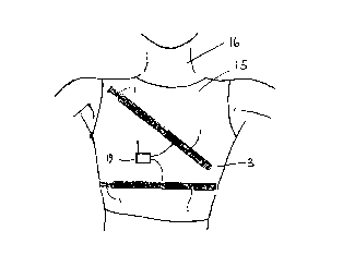
Figure 8 is a pictorial depiction of the belt of
Figure 7 in place over the chest of a patient.
Figure 9 is a pictorial version of a garment worn by
a patient that carries four pick-up electrodes.
DESCRIPTION OF THE PREFERRED EMBODIMENT
In Figure lA a schematic is shown of an electrical
sensor system incorporating a pick-up electrode 1 in the form
of a flat conductive surface placed adjacent a first location
13
CA 02280996 1999-08-26
2 on a body 3 where an electrical signal is to be sensed
originating from an electrical signal generator 4 within the
body 3 that provides a source voltage Vs. The pick-up
electrode 1 develops a capacitive coupling to the body 3
through an intervening dielectric layer separating it from the
body 3. This capacitive coupling for the pick-up electrode 1
is represented schematically by the capacitor Cp.
The electrode 1 is connected to the input of an
operational amplifier - IC1A, or its equivalent such as a
field effect transistor. High resistance diodes D1, connected
to the electrode 1 in parallel if high resistance at low
forward voltage diodes are used, or in series otherwise, have
an effective leakage value of on the order of 1012 ohms at low
voltage and serve to discharge the electrode and restore
proper voltage input levels. Diodes D1, if in parallel
format, also serve to protect the operational amplifier IClA
from excessive input voltages.
The output Vo from the operational amplifier IC1A is
measured across output resistor Rl that extends between the
output of the operational amplifier IC1A and a reference
capacitor CR that is coupled to the body at a second, separate
location 5. This location 5 may be separated from the first
location 2 in obtaining conventional ECG signals. The
locations 2,5 may also be proximate, e.g. adjacent, at certain
body locations and still provide useful signals. In such
14
CA 02280996 1999-08-26
arrangement signals are obtained effectively from virtually a
single location.
Capacitive coupling CR is effected by means of an
electrode (not shown in Figure 1A) that is separated from the
body 3 by a non-conducting material that acts as a dielectric.
Conveniently, the case for an on-board battery holder can
serve as this electrode, as shown further below.
Inside the body 3, the signal generator 4 is seen as
being subject to internal resistance RB within the body 3.
The circuit of Figure 1A is redrawn as Figure 1B in
more conventional form. In Figure 1B, the capacitance Co
arises from the combined input capacitance of the operational
amplifier IC1A and the diodes D1. The input resistance of
this amplifier is represented by Ro, including the resistive
value of the diodes D1. Collectively, the capacitances C~, Co,
CR act as a voltage divider network whereby the output voltage
Vo is proportional to the source voltage VS . In Figures 2A and
2B, the coupling to the body 3 at the end of the voltage
divider network opposite to the pick-up electrode 1, is
effected principally by a direct, conductive contact. The
resistance of the interface is indicated by RR. Necessarily,
some slight capacitance coupling is also still present,
indicated by C1R
In Figure 5 a graphic plot is depicted of the
variation of capacitance C with a variation in the separation
CA 02280996 1999-08-26
distance d at various separation distances d, based upon the
theoretical formula: C =k.A
a
where: C is the effective capacitance of, for example CP,
d is the separation distance of the electrode plate
from the body giving rise to the capacitance,
A is the area, or effective area, of the pick-up
electrode 1; and
k is a proportionality constant affected by the
dielectric material in the separation gap.
Four curves are shown in Figure 5 for pick-up
electrodes 1 having surface areas as follows:
a = 1 cm2 c = 50 cm2
b = 10 cm2 d = 10 0 cm2
Each capacitance curve can be separated into two
important regions: region 6, in which the capacitance chances
relatively rapidly with a given change in separation distance;
and region 8 in which the capacitance changes relatively
slowly with a similar given change in separation distance.
These regions are separated on Figure 5 by boundary line 7.
For capacitors with an electrode area of around 25 cm2 and
capacitive values below 200 picofarads, region 6 approximately
corresponds to the zone with d = 0.1 mm or less; while for
such values region 8 approximately corresponds to the values
above d = 0.1 mm.
16
CA 02280996 1999-08-26
An important implication of Figure 5 is that sensors
with capacitance values within regime 6 are very sensitive to
small additional changes in the separation distance (delta-d).
In contrast, sensors with capacitance values corresponding to
region 8 are relatively insensitive to such changes. This is
illustrated more succinctly in Figure 6.
In Figure 6, the percentage change in capacitance
corresponding to a delta-d = 0.1 mm is graphed as a function
of the nominal separation distance d.
Figure 6 is dimensionless along the C axis and
applies to all capacitive sensors which obey or approximately
obey the relation C=kA/d. According to the invention the
capacitive value of the pick-up electrode, and other
capacitive sensors when employed, are designed to operate in
region 8' of Figure 6, as opposed to region 6' from which it
is separated by boundary line 7'.
In this latter regime the capacitance, and hence
the output signal is sufficiently insensitive to spatial and
temporal body surface variations so as to provide the
advantages of signal stability inherent in the invention.
In Figure 3 two pick-ups similar to that of Figure
lA are used to drive a differential amplifier IC3A. The
additional electrode 1A is placed at a further location 10,
separated from the first and second locations 2,5. Within the
17
CA 02280996 1999-08-26
body the signal source vs may be treated as distributing its
potential over the resistors RB, R'B, R"H.
By use of this differential signal detection
circuit, common mode noise present in the two pick-up circuits
will be eliminated.
Figure 4 shows the circuit of Figure 3 extended by
an optical isolator ISO1 driven by a buffer operational
amplifier IC4A. By mounting these circuits as close as
possible to the pick-up electrode 1, interference from ambient
60 Hz electromagnetic signals can be minimized.
In Figure 4, a shielding conductive layer 11 is
depicted as overlying the externally-directed side of the
circuitry. This layer/structure 11 is preferably connected to
the circuit common point. Its role is to exclude effects
arising from intruding electro-magnetic signals, e.g. 60Hz,
originating in the environment.
In Figure 7 a belt 12 is depicted that carries the
circuit of Figure 4. The pick-up electrodes 1 are mounted on
a MYLAR~T"'~ or KAPTON~TM~ film 13 that serves both as a spacer
and as an insulating dielectric of approximately 0.13 mm
thickness. The pick-up electrodes 1 have been measured
against a copper plate as providing a capacitance value of 20
picofarads.
It is preferable for the insulating layer to have a
thickness which is equal to, or grater than, the size of
18
CA 02280996 1999-08-26
surface irregularities of the body being measured, and equal
or greater than the variations in the sensor-to-body
separation gap.
The belt 12 of Figure 7 has its own on-board power
supply in the form of batteries 14. The case 15 of the
batteries 14 is connected to circuit common point and serves
as an electrode to provide the reference capacitor CR. A
measured value for its capacitance, when placed against a
copper plate, of 160 picofarads has been observed with the
case 15 coupled to the entire circuit. The substrate for the
belt 12 is made of KAPTON~TM~ having a thickness of 5
thousandths of an inch. This forms the principal dielectric
element for both of the capacitors Cp, CR. The nature of the
dielectric material has little effect on the invention when
the pick-up electrodes are located at a sufficient "stand-off"
gap from the body.
The shield 11 in the belt 12 of Figure 7 is in the
form of a flexible conductive layer, with an insulated
undersurface that overlies the circuitry on the outer side
portion of the belt 12.
The pick-up electrodes 1 in Figure 4 are held by the
substrate 13 of the belt 12, at a fixed, intervening interval.
This interval is dimensioned to permit the electrodes 1 to
respectively overlie electrical nodes (not shown) on the body
3 of a wearer 16 as shown in Figure 8. The belt 12 is held in
19
CA 02280996 1999-08-26
place by tension developed by connectors, e.g. hook-and-loop
fastening means, once positioned on the body 3. While a
narrow belt 12 is depicted in figure 8, a wider belt or vest
15 could carry three or more electrodes 1 as shown in Figure
9.
An advantage of the invention is that multiple pick-
up electrodes can be assembled in a preformatted, fixed array
that can be fitted to the body collectively, as a unitary
assembly, much as in the manner of donning an article of
clothing. This permits a wearer to be "fitted-up" for
electrical field measurement in a very short period of time.
Data acquisition can readily be suspended and resumed by the
simple act of removing and then re-donning the pre-assembled
array. No components are consumed in this process.
The electrodes 1 of such a piece of apparel may feed
signals to a radio transmitter 19 carried by the wearer 16.
In this manner an especially convenient form of tele-
monitoring can be achieved.
CONCLUSION
The foregoing has constituted a description of
specific embodiments showing how the invention may be applied
and put into use. These embodiments are only exemplary. The
invention in its broadest, and more specific aspects, is
further described and defined in the claims which now follow.
CA 02280996 1999-08-26
These claims, and the language used therein, are to
be understood in terms of the variants of the invention which
have been described. They are not to be restricted to such
variants, but are to be read as covering the full scope of
the invention as is implicit within the invention and the
disclosure that has been provided herein.
21