Note: Descriptions are shown in the official language in which they were submitted.
CA 02281448 1999-08-25
. ..
V
HIGH FREQUENCY LOW LOSS ELECTRODE
BACKGROUND OF THE INVENTION
1. Field of the Invention
The present invention relates to a high frequency low loss
electrode for use in transmission lines and resonators operative
in a microwave band and a millimeter wave band which are used
mainly in radio communication, a transmission line, a high
frequency resonator, a high frequency filter, an antenna common
device, and a communication equipment each including the. high
frequency low loss electrode.
2. Description of the Related Art
In microwave IC' s and monolithic microwave IC' s operated
at a high frequency, used generally are strip-type transmission
lines and microstrip-type transmission lines which can be easily
produced and of which the size and weight can be reduced. As
a resonator for such uses, one in which the above-described line
is set at a length equal to a quarter-wavelength or a half-
wavelength, or a circular resonator containing a circular
conductor are employed. The transmission loss of these lines
and the unloaded Q of the resonators are determined mainly by
the conductor loss. Accordingly, the performance of the
microwave IC' s and the monolithic microwave IC' s depends on how
much the conductor loss can be reduced.
These lines and resonators are formed with conductors with
CA 02281448 1999-08-25
- 2 -
a high conductivity such as copper, gold, or the like. However,
the conductivities of metals are inherent to the materials.
There is a limitation in a method of selecting a metal with a
high conductivity, and forming the metal into an electrode to
reduce the loss. Accordingly, great attention has been given
to the fact that at the high frequency of a microwave or a
millimeter wave, a current is concentrated onto the surface of
an electrode, caused by the skin effect, and most of the loss
occurs in the vicinity of the surface (end portion) of the
conductor. It has been investigated to reduce the conductor loss
from the standpoint of the structure of the electrode. For
example, in Japanese Unexamined Patent Publication 8-321706,
disclosed is the structure in which plural linear conductors with
a constant width are arranged in parallel to the propagation
direction at constant intervals to reduce the conductor loss.
Moreover, in Japanese Unexamined Patent Publication 10-13112,
disclosed is the structure in which the end portion of an
electrode are divided into plural parts, so that a current
concentrated at the end portion is dispersed to reduce the
conductor loss.
However, the method by which the whole of an electrode
is divided through plural conductors having an equal width as
disclosed in Japanese Unexamined Patent Publication8-321706has
the problem that the effective cross-sectional area of the
electrode is decreased, so that the conductor loss cannot be
CA 02281448 2002-04-02
effectively reduced.
Moreover, a~:, regards the method in which the end of
the electrode ~.s divided inl:o plural sub-conductors
having substantia:Lly the same width as disclosed in
Japanese Unexami~ae~d Patent Publication 10-13112, it is
effective to some degree in relaxing the current
concentration and reducing the conductor loss. However,
it can not be recognized that the effect is satisfactory.
SUMMARY OF THE INVENTION
Accordingly, i.t is an object of an aspect of the
present invention to provide a high frequency low loss
electrode of which the conductor loss can be reduced
effectively, suff:ic~iently.
It is anotl-~.e:r obj ect of an aspect of the present
invention to provide a transmission line, a high
frequency resonator, a high frequency filter, an antenna
common device, and a communication equipment each
including the above-described high frequency low loss
electrode and hawing a low loss.
The present invention has been achieved based on a
finding that in an e:Lectrode having an end portion
divided into plural sub-conductors, the conductor loss
can be effectively redu~~ed by setting the widths of the
sub-conductors ac°cording to a principle.
According to an aspect. of the present invention,
there is provided a first high frequency low loss
electrode which comprises a main
CA 02281448 1999-08-25
> ..
- 4 -
conductor, and at least one sub-conductor formed along a side
of the main conductor, at least one of the sub-conductors having
a multi-layer structure in which thin-film conductors and
thin-film dielectrics are laminated alternately.
Preferably, in the first high frequency low loss electrode
of the present invention, the sub-conductor positioned nearest
to the outside of the sub-conductors has a width smaller than
(~c/2 ) times the skin depth b at an applied frequency. Accordingly,
an ineffective current in the sub-conductor positioned nearest
to the outside can be reduced. More preferably, in order to
reduce an ineffective current in the sub-conductor positioned
nearest to the outside, the width of the sub-conductor is set
at a value smaller than (~c/3 ) times the skin depth S at an applied
frequency.
More preferably, in the first high frequency low loss
electrode of the present invention, when the high frequency low
loss electrode includes the plural sub-conductors, the width of
each of the sub-conductors is smaller than (~c/2 ) times the skin
depth b at an applied frequency.
Still more preferably, in the first high frequency low
loss electrode of the present invention, when the high frequency
low loss electrode includes the plural sub-conductors, the
plural sub-conductors are formed so that a sub-conductor thereof
positioned nearer to the outside is thinner. Accordingly, the
conductor loss can be effectively reduced.
CA 02281448 2002-04-02
-
Further, in the first high frequency low loss electrode
of the present invention, sub-dielectrics may be provided
between the main conductor and the sub-conductor adjacent to the
main conductor and :between adjacent sub-conductors,
respectively.
Preferably, in the first high frequency low loss electrode
of the present invention, the interval between the main conductor
and the sub-conductor- adjacent to the main conductor and the
intervals between adjacent sub-conductors are formed so that an
interval thereof positioned nearer to the outside is shorter,
correspondingly to the widths of the respective adjacent
sub-conductors, in order that currents substantially in phase
are made to flow through the sub-conductors.
Further, in they first high frequency low loss electrode
of the present invention, when the high frequency low loss
electrode includes the sub-dielectrics, the plural sub-
dielectrics may be farmed so that a sub-dielectric thereof
positioned nearer to the outside has a lower dielectric constant.
Preferably, in the first high frequency low loss electrode
of the present invention, the thin-film conductors in the
sub-conductor having a multi.-layer structure are formed so that
a thin-film conductor thereof lying at a further inside position
is thicker.
According to another aspect of the present invention,
there is provided a high frequency low loss electrode which
comprises a main
CA 02281448 1999-08-25
- 6 -
conductor, and plural sub-conductors formed along a side of the
main conductor, the sub-conductors being formed so that a
sub-conductor thereof positioned nearer to the outside has a
smaller width, at least one of the sub-conductors having a
multi-layer structure in which thin-film conductors and
thin-film dielectrics are laminated alternately.
Preferably, in the second high frequency low loss
electrode of the present invention, at least one of the sub-
conductors is set at a width smaller than (~/2) times the skin
depth 8 at an applied frequency in order to reduce the ineffective
current.
More preferably, in the second high frequency low loss
electrode of the present invention, at least one of the sub-
conductors is set at a width smaller than (~/3 ) times the skin
depth b at an applied frequency in order to reduce a more
ineffective current.
Also, in the second high frequency low loss electrode of
the present invention, sub-dielectrics may be provided between
the main conductor and the sub-conductor adjacent to the main
conductor and between adjacent sub-conductors, respectively.
Preferably, in the second high frequency low loss
electrode of the present invention, the interval between the main
conductor and the sub-conductor adjacent to the main conductor
and the intervals between adjacent sub-conductors are set so that
an interval thereof positioned nearer to the outside is shorter,
CA 02281448 2002-04-02
- 7 -
correspondingly to the widths of 'the respective adjacent
sub-conductors in order that currents substantially in phase are
made to flow through the sub-conductors.
More preferab:Ly, in the second high frequency low loss
electrode of the present invention, the dielectric constants of
the plural sub-dielectrics are set so that the dielectric
constant of a sub-dielectric positioned nearer to the outside
of the plural sub-d:ielectrics is lower, correspondingly to the
widths of the adjacent sub-conductors in order that currents
substantially in phase are made to flow through the respective
sub-conductors.
Still more preferably, in the second high frequency low
loss electrode of the present invention, in the sub-conductor
having a mufti-layer structures the thin-film conductors are
formed so that a thi.n~-film conductor thereof lying at a further
inside position is thicker. Accordingly, the conductor loss of
the sub-conductors having a mufti-layer structure can be
reduced.
According to yet another aspect of the present invention,
there is provided. a high frequency low loss electrode which
comprises a main conductor and plural sub-conductors formed
along a side of the main conductor, the sub-conductors
excluding at least he sub-conductor positioned nearest to the
outside of the sub-conductors having a mufti-layer structure
in which thin-film conductors anal thin-film dielectrics are
laminated alternately,
CA 02281448 1999-08-25
$ -
the sub-conductors being formed so that a sub-conductor thereof
positioned nearer to the outside has the less number of laminated
thin-film conductors.
Preferably, in each of the first through third high
frequency low loss electrodes of the present invention, the main
conductor is a thin-film multi-layer electrode comprising
thin-film conductors and thin-film dielectrics laminated
alternately.
Preferably, in each of the,first through third high
frequency low loss electrodes of the present invention, at least
one of the main conductor and the sub-conductors is made of a
superconductor.
The first high frequency resonator of the present
invention includes any one of the first through third high
frequency low loss electrodes of the present invention.
Further, the first high frequency transmission line of
the present invention includes any one of the first through third
high frequency low loss electrodes of the present invention.
Preferably, the second high frequency resonator of the
present invention includes the first high frequency transmission
line of which the length is set at a quarter-wavelength multiplied
by an integer.
More preferably, the third high frequency resonator of
the present invention includes the above-described first high
frequency transmission line of which the length is set at a
. . CA 02281448 1999-08-25
_ g _
half-wavelength multiplied by an integer.
The high frequency filter of the present invention
includes any one of the first through third high frequency
resonators.
The antenna common device of the present invention
includes the. high frequency filter.
Further, characteristically, the communication
equipment of the present invention includes one of the high
frequency filter and the antenna common device.
BRIEF DESCRIPTION OF THE DRAWINGS
FIG. 1 is a triplet type strip line including a high
frequency low loss electrode according to an embodiment of the
present invention;
FIG. 2 is a graph showing the attenuation of a current
density inside a conductor;
FIG. 3 illustrates the phase change of a current density
inside of a conductor;
FIG. 4 illustrates the phase change of a current density
when conductors and dielectrics are alternately arranged;
FIG. 5A is a perspective view of a triplet type strip line
model for analysis of a multi-line structure electrode according
to the present invention;
FIG. 5B is an enlarged cross-sectional view of the strip
conductor in the model of FIG. 5A;
CA 02281448 2002-04-02
- 10 -
FIG. 5C is a still enlarged cross-sectional view of the
strip conductor;
FIG. 6 is a two-dimensional equivalent circuit diagram of
the multi-layer mult.i-line model of FIG. 5C;
FIGS. 7A anti 7B are one-dimensional equivalent circuit
diagrams, each circuit diagram being in one direction of the
multi-layer multi-line model of F:IG. 5C;
FIG. 8 is a perspective view of a triplet type strip line
model used in the simulation of the multi-line structure
electrode according to the present invention;
FIG. 9A is a view of a conventional electrode not having
a multi-line structure used in the simulation;
FIG. 9B illusi:rates the simulation results of the electric
field distribution;
FIG. 9C illustrates the simulation results of the phase
distribution;
FIG. 10 illustrates an electrode having a multi-line
structure according to the present. invention used in the
simulation;
FIG. 11A illustrates the simulation results of an electric
field distribution i:n the electrode of FIG. 10;
FIG. 11B illustrates the simulation results of a phase
distribution in the electrode of fig. 10;
FIG. 12 is a cross-sectional view showing the
configuration of a high frequency low loss electrode of the
modification example 1;
CA 02281448 1999-08-25
- 11 -
FIG. 13 is a cross-sectional view showing the
configuration of a high frequency low loss electrode of the
modification example 2;
FIG. 14 is a cross-sectional view showing the
configuration of a high frequency low loss electrode of the
modification example 3;
FIG. 15 is a cross-sectional view showing the
configuration of a high frequency low loss electrode of the
modification example 4;
FIG. 16 is a cross-sectional view showing the
configuration of a high frequency low loss electrode of the
modification example 5;
FIG. 17 is a cross-sectional view showing the
configuration of a high frequency low loss electrode of the
modification example 6;
FIG. 18 is a cross-sectional view showing the
configuration of a high frequency low loss electrode of the
modification example 7;
FIG. 19 is a cross-sectional view showing the
configuration of a high frequency low loss electrode of the
modification example 8;
FIG. 20 is a cross-sectional view showing the
configuration of a high frequency low loss electrode of the
modification example 9;
FIG. 21 is a cross-sectional view showing the
CA 02281448 1999-08-25
- 12 -
configuration of a high frequency low loss electrode of the
modification example 10;
FIG. 22 is a cross-sectional view showing the
configuration of a high frequency low loss electrode of the
modification example 11;
FIG. 23 is a cross-sectional view showing the
configuration of a high frequency low loss electrode of the
modification example 12;
FIG. 24 is a cross-sectional view showing the
configuration of the high frequency low loss electrode of the
modification example 13 of the present invention;
FIG. 25 is a cross-sectional view showing the
configuration of the high frequency low loss electrode of the
modification example 14 of the present invention;
FIG. 26 A is a perspective view showing the configuration
of a circular strip resonator which is an application example
1 of a high frequency low loss electrode according to the present
invention;
FIG. 26B is a perspective view showing the configuration
of a circular resonator wick is an application example 2 of a
high frequency low loss electrode according to the present
invention;
FIG. 26C is a perspective view showing the configuration
of a microstrip line which is an application example 3 of a high
frequency low loss electrode according to the present invention;
CA 02281448 1999-08-25
". .
- 13 -
FIG. 26D is a perspective view showing the configuration
of a coplanar line which is an application example 4 of a high
frequency low loss electrode according to the present invention;
FIG. 27A is a perspective view showing the configuration
of a coplanar strip line which is an application example 7 of
a high frequency low loss electrode according to the present
invention;
FIG. 27B is a perspective view showing the configuration
of a parallel slot line which is an application example 6 of a
high frequency low loss electrode according to the present
invention;
FIG. 27C is a perspective view showing the configuration
of a slot line which is an application example 7 of a high
frequency low loss electrode according to the present invention;
FIG. 27D is a perspective view showing the configuration
of a high impedance microstrip line which is an application
example 8 of a high frequency low loss electrode according to
the present invention;
FIG. 28A is is a perspective view showing the
configuration of a slot line which is an application example 7
of a high frequency low loss electrode according to the present
invention;
FIGS. 28B and 28C are perspective views each showing the
configuration of a half-wave type microstrip line resonator
which is an application example 10 of a high frequency low loss
CA 02281448 1999-08-25
- 14 -
electrode according to the present invention;
FIG. 28D is a perspective view showing the configuration
of a quarter-wave type microstrip line resonator which is an
application example 11 of a high frequency low loss electrode
according to the present invention;
FIGS. 29A and 29B are plan views showing the configuration
of a half-wave microstrip line filter which is an application
example 12 of a high frequency low loss electrode according to
the present invention;
FIG. 29C is a plan view showing the configuration of a
circular strip filter which is an application example 13 of a
high frequency low loss electrode according to the present
invention;
FIG. 30 is a block diagram showing the configuration of
a duplexer 700 as an application example 14; and
FIG. 31 illustrates the configuration of an application
example including the duplexer 700 of FIG. 30.
DESCRIPTION OF THE PREFERRED EMBODIMENT
Hereinafter, a high frequency low loss electrode
according to an embodiment of the present invention will be
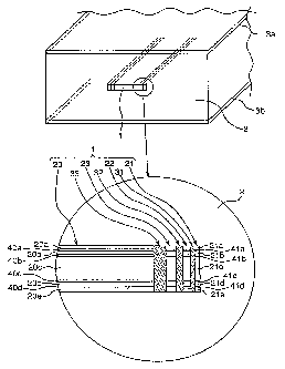
described. FIG. 1 shows a triplet type strip line including the
high frequency low loss electrode 1 of the embodiment. The strip
line has the configuration in which the high frequency low loss
electrode 1 having a predetermined width is formed in the center
CA 02281448 1999-08-25
- 15 -
of a dielectric 2 with a rectangular cross-section, and ground
electrodes 3a and 3b are formed in parallel to the high frequency
low loss electrode 1. In the high frequency low loss electrode
1 of this embodiment, as shown in the enlarged view of ~'IG. 1,
the end portion is divided into sub-conductors 21, 22, and 23,
so that an electric field concentrated in the end portion is
dispersed, and the conductor loss at a high frequency is reduced.
In this embodiment, the sub-conductors 21, 22, and 23 are formed
to have a lamination structure in which thin-film conductors and
thin-film dielectrics are laminated alternately, and thereby,
the conductor loss in the sub-conductors 21, 22, nd 23 is reduced,
that is, the conductor loss in the end portion of the high
frequency low loss electrode is reduced.
In particular, in the high frequency low loss electrode
1 of this embodiment, the sub-conductor 23 is formed to be
adjacent to the main conductor 20 through a sub-dielectric 33.
The sub-dielectric 32, the sub-conductor 22, the sub-dielectric
31, and the sub-conductor 21 are formed sequentially toward the
outside in that order. The sub-conductors 23, 22, and 21 are
formed so that the width of a sub-conductor thereof positioned
nearer to the outside (more distant from the main conductor) is
smaller to reduce the conductor loss of all the sub-conductors,
the sub-conductors 21, 22, and 23 are formed to have a width of
up to ~c/2 times the skin depth b at an applied frequency, and
the respective widths of the sub-dielectrics 33 , 32 , and 31 are
CA 02281448 1999-08-25
i
- is -
set so that currents substantially in phase flow through the
respective sub-conductors 21, 22, and 23. Accordingly, the
concentration of an electric field in the end portion of the
electrode, caused when no sub-conductors are provided, can be
effectively dispersed in the respective sub-conductors 21, 22,
and 23.
Further, the sub-conductor 21 has a multi-layer structure
in which a thin-film conductor 21a, a thin-film dielectric 41a,
a thin-film conductor 21b, a thin-film dielectric 41b, a
thin-film conductor 21c, a thin-film dielectric 41c, a thin-
film conductor 21d, a thin-film dielectric 41d, and a thin-film
conductor 21e are laminated.
In the sub-conductor 21, the thin-film conductors 21a,
21b, 21c, 21d, and 21e are formed so that a thin-film conductor
thereof lying at a further inside position is thicker, in order
that the conductor loss of the sub-conductor is reduced. The
film-thicknesses of the thin-film dielectrics 41a, 41b, 41c, and
41d are set so that currents substantially in phase flow through
the thin-film conductors 21a, 21b, 21c, 21d, and 21e,
correspondingly. In this embodiment, the sub-conductors 22 and
23 are formed in the same manner as the sub-conductor 21.
The film-thicknesses of the thin-film conductors21a,21b,
21c, 21d, and 21e which are preferable for reduction of the
conductor loss of the sub-conductors, and the film-thicknesses
of the thin-film dielectrics 41a, 41b, 41c, and 41d which are
CA 02281448 1999-08-25
- 17 -
preferable to be made to flow currents substantially in phase
through the thin-film conductors 21a, 21b, 21c, 2Id, and 21e will
be described later.
Hereinafter, as regarding the high frequency low loss
electrode 1 of this embodiment, a method of setting the
line-widths of the sub-conductors and the widths of the sub-
dielectrics will be described.
1. Currents and Phases in Respective Sub-conductors
(Current Densities and Phases in Conductor Insides)
In general, the current density function J(z) inside a
conductor is expressed by the following mathematical formula 1,
caused by the skin effect which occurs at a high frequency. In
the mathematical formula 1, z represents a distance in the depth
direction from the surface taken as the reference (0), and 8
represents the skin depth at an angular frequency cu (= 2~cf ) which
is expressed by the mathematical formula 2. Further, cf
represents a conductivity, and ~,o a permeability in vacuum.
Accordingly, inside of the conductor, the current density is
decreased at a position deeper from the surface as shown in FIG.
2.
[mathematical formula 1]
J( z )=JQe-~~+»=ia (A~m2 )
[mathematical formula 2]
8 = 2 / wl~oo
Accordingly, the absolute value of the amplitude of the
CA 02281448 1999-08-25
>~
- 18 -
current density is expressed by the following mathematical
formula 3, and is attenuated to 1/e at z = b. The phase of the
amplitude of the current density is expressed by the mathematical
formula 4. As z is increased (namely, at a position deeper from
the surface) , the phase is increased on the minus side, and at
z = 8 ( surface skin depth ) , the phase is decreased by 1 rad ( about
60°) as compared with that at the surface.
[mathematical formula 3]
abs(J(z)) =~Jo~e-Z~a
[mathematical formula 4]
arg(J(z))=-z/S
Accordingly, a power loss P1°$$ is expressed by the
following mathematical formula 5 using resistivity p = 1/a. The
overall power loss P°lo8$ of a conductor which is sufficiently thick
is expressed by the formula 6. At z = b, (1-a Z) of the overall
power loss P°1°s8, namely, 86.5 ~ is lost.
[mathematical formula 5]
P~°ss = ~ PIJ(z)I2dz (p =1 / cs: resistivity)
= pIJ o I2 8 / 2(1- e-ZZis )
[mathematical formula 6]
2
Poi°SS = PIJoI b J 2
Further, by using the current density function J ( z ) , the
surface current K is given by the following mathematical formula
7. The surface current K is a physical quantity which is
CA 02281448 1999-08-25
- 19 -
coincident with the tangential component of a magnetic field
(hereinafter, referred to as a surface magnetic field) at the
surface of a conductor. The surface current K is in phase with
the surface magnetic field, and has the same dimension as the
surface magnetic field, namely, the dimension of A/m.
[mathematical formula 7]
K= fo J(z)dz=say+~~
As seen in the mathematical relation formula 7, the phase
of the current density Jo at the surface is 45°, if observed at
the time when the phase of the surface current K (namely, the
surface magnetic field) is 0°, Accordingly, the phase of the
current density function J(z) inside the conductor can be
illustrated by a model as shown in FIG. 3. Further, when the
phase of the current density Jo is 45°, the surface current K is
given by the following formula 8.
[mathematical formula 8]
K=~K~=s~Jo~~~
Assuming that the phase of the current density amplitude
is not changed with the depth ( behaviors like direct current ) ,
the surface current is expressed by following formula 9.
[mathematical formula 9~
K.= r0 IJoIe-zisdz
= slJol
CA 02281448 1999-08-25
- 20 -
As understood by the comparison of the formulae 8 and 9,
the surface current K at a high frequency is decreased to be 1/~
- 70.7 as compared with the surface current K' of the direct
current. It is speculated that this is because an ineffective
current flows . In fact, it can be recognized that the overall
power loss calculated based on the formula 9 can be expressed
by the formula 5.
On the other hand, if the current density expressed by
the formula 9 is multiplied by 1 / ~ so that the surface currents
are equal to each other, the overall power loss, on the condition
that the equal surface currents are realized, will be (1/~)Z
- 1 /2 = 50
Accordingly, under the ideal limit condition that the
phases of the current densities are made equal to 0°, and the
phases suffer no changes inside the conductor, the power loss
can be reduced to 50~. Practically, since the phase of the
current density is decreased inside the conductor, it is
difficult to realize the above-described ideal state.
(Current and Phase in Each Sub-conductor)
However, in the multi-line structure in which sub-
conductors and sub-dielectrics are alternately arranged, the
periodic structure in which the phase is changed periodically
in the range of ~ 8 as shown in FIG. 4 can be realized by utilization
of the phenomena that the phase of a current density inside a
dielectric increases. That is, characteristically, in the high
CA 02281448 1999-08-25
- 21 -
frequency low loss electrode 1 of this embodiment, realized is
the structure in which the phases of the current densities inside
the sub-conductors are changed periodically in a relative small
range with respect to the center of 0, by setting 8 at a small
value in the above-described periodic structure, and thereby,
an ineffective current is reduced.
Accordingly, the following two points as requirements to
be preferred and satisfied for the high frequency low loss
electrode 1 of this embodiment can be derived from the
above-described discussion.
( 1 ) The line-width of each sub-conductor is set so that
the change width ( 28 ) of the current density phase is small . As
seen in the above description, as the line-width of the sub-
conductor is narrower, the change width of the phase can be more
reduced to reach the above-described ideal state. Practically,
in consideration of the manufacturing cost, the phase is set
preferably at 8 s 90°, and more preferably at 8 s 45°.
The setting at 8 s 90° can be achieved by setting the line
width of each sub-conductor at ~cb/2 or lower. Further, the
setting at 8 s 45° can be made by setting the line-width of each
sub-conductor at ~S/4 or lower.
( 2 ) The widths of the sub-dielectrics are set so that the
changed current density phases in the respective sub-conductors
lying on the current-approaching side are cancelled out.
2. Processing of Multi-Zine Structure by Equivalent
CA 02281448 1999-08-25
f
- 22 -
Circuit
Hereinafter, the multi-line structure of the high
frequency low loss electrode 1 of the present invention will be
described in reference to a simplified modeled structure.
FIG. 5A shows a triplet type strip line model which can
be analyzed relatively easily, and will be used in the following
description. The model has the configuration in which a strip
conductor 101 with a rectangular cross-section is provided in
a dielectric 102. The strip conductor 101 is configured so that
the cross-section is symmetric with respect to right and left
and upper and lower sides as shown in FIG. 5B. Further, as shown
in FIG. 5C, the strip conductor 101 has the multi-line structure
in an end portion thereof, and is composed of multi-layers in
the thickness direction. More particularly, the strip
conductor 101 is composed of many sub-conductors, and has the
matrix structure in which the sub-conductors ( 1, 1 ) , ( 2 , 1 ) , ( 3 ,
1) ... are arranged in the thickness direction, and the sub-
conductors ( 1, 1 ) , ( 1, 2 ) , ( 1, 3 ) . . . are arranged in the width
direction.
The two-dimensional equivalent circuit as shown by the
multi-layer multi-line model in FIG. 5C can be expressed as in
FIG. 6. In FIG. 6, Fcx represents the cascade connection matrix
of the conductors in the width direction thereof, and Fcy the
cascade connection matrix of the conductors in the thickness
direction thereof. The codes (1, 1), (1, 2) ... , which
CA 02281448 1999-08-25
- 23 -
correspond to the respective sub-lines, are appended to Fcx and
Fcy.
Ft represents the cascade connection matrix of the
dielectric layers in the respective lines. The dielectric
layers are numbered sequentially from the uppermost layer. Fs
represents the cascade connection matrix of the adjacent
conductor lines in the width direction, and numbered
sequentially from the outside. The respective cascade
connection matrixes Fcx, Fcy, Ft, and Fs are expressed by the
following formulae 10 through 13. In the formulae 10 through
13, L and g represent the width and the thickness of each
sub-conductor, and S the width of the sub-dielectric between
adjacent sub-conductors. Accordingly, the cascade connection
matrixes Fcx, Fcy, Ft, and Fs correspond to the widths and the
thicknesses of the respective sub-conductors, and the widths of
the respective sub-dielectrics. In this case, Zs represents the
surface (characteristic) impedance of each conductor, and
expressed by Zs = ( 1 + j ) ~/~ ( cu~,o ) / ( 2a) } .
(mathematical formula 10]
cosh' 1 S ~ ~ 2 J Zs sinh C l b J ~ 2
F~ \_ f
sinhl 1 s J ~ 2~ cosh~l s ~ ~ 2~
[mathematical formula 11~
CA 02281448 1999-08-25
,.s
- 24 -
cosh) 1 S ~ ~ ZJ Zssinhl l S' ~ 2~
F~y \ \- ' 1
sink/ 1 s ~ ~ 2J cash~l s J 2)
[mathematical formula 12]
Ft ~ 1 J~l~ot~1- Em l
t
0 1
[mathematical formula 13~
Jwf~osC1- ES
0 1
Accordingly, theoretically, the line width L and the
thickness g of the respective sub-conductors, and the width S
and the thickness t of the respective sub-dielectrics may be set
so that the real part (resistance component) of the surface
impedance of the respective sub-conductors is minimum, by
operating the connection matrixes based on the two-dimensional
equivalent circuit of FIG. 6.
However, it is difficult to determine analytically the
line width L and the thickness g of the respective sub-conductors,
and the width S and the thickness t of the respective sub-
dielectrics based on the two-dimensional equivalent circuit of
FIG. 6 and in the above-described conditions.
Accordingly, by the inventors, by using the equivalent
circuit of FIG. 7 which is the one-dimensional model in the width
CA 02281448 1999-08-25
- 25
direction of the equivalent circuit of FIG. 6, the recurrence
formula expressed by the formula 14 is obtained on the condition
that the real part (resistance component) of the surface
impedance of the respective sub-conductors is minimum. The line
width L of the respective sub-conductors and the width S of the
respective sub-dielectrics are set based on the parameter b
satisfying the recurrence formula and the formulae 15 and 16.
The equivalent circuit of FIG. 7 is the one-dimensional model
in which the equivalent circuit of FIG. 6 is taken as a single
layer, and the thickness direction of the single layer is not
considered.
[mathematical formula 14~
bk+1 = tanh-1 ( tan bk )
[mathematical formula 15]
Lk+1 - Lk ( bk+1 ~ bk )
[mathematical formula 16]
Sk+1 - Sk ( bk+1 ~ bk )
As described above, the line-width L of the respective
sub-conductors and the width S of the respective sub-dielectrics
were set, and the conductor loss at a high frequency was evaluated
by a finite element method. It has been identified that the loss
can be reduced as compared with the case where the line-width
L of the respective sub-conductors and the width S of the
respective sub-dielectricsareset at equal values, respectively.
When the line-width L of the respective sub-conductors and the
CA 02281448 1999-08-25
._
- 26 -
width S of the respective sub-dielectrics are set, it is necessary
to give the initial values of b1, L1, and S1 previously. In this
invention, it is preferable that the initial values are set so
that the electric current phases of the respective current
densities are in the range of ~ 90° or ~ 45°. As a result of the
analysis using the one-dimensional model of FIG. 7A, a
satisfactory relationship a.s derived between L1 and S1 to which
initial values are to be given, in order to minimize the surface
resistance. The initial values are given to Ll and S1 so as to
satisfy the relationship, so that currents substantially in
phase flow through the respective sub-conductors. That is, by
the examination from the circuit theoretical standpoint, it is
concluded that the preferable condition which the widths of the
respective dielectrics are to satisfy is "the widths of the
sub-dielectrics are set so that the changed current density
phases in the sub-conductors on the current-approaching side are
cancelled out". Thus, the same results as the conditions
described in (2) of Paragraph Number (0039) can be obtained.
Further, by the inventors, the line-width L of the
respective sub-conductors and the width S of the respective
sub-dielectrics are set by using the following mathematical
formulae 17 and 18 which are decreasing functions analogous to
the recurrence formula of the mathematical formula 14 , instead
of the formula 14. The conductor loss at a high frequency was
evaluated by the finite element method. As a result, it has been
CA 02281448 1999-08-25
- 27 -
identified that in the above-described manner, the loss can be
reduced as compared with the case where the line-widths of the
sub-conductors and also, the widths S of the sub-dielectrics are
set at the same values, correspondingly.
[mathematical formula 17]
bx+i = tarih-1 bx
[mathematical formula 18~
bx+i = tan bx
The results obtained by use of the respective formulae
14 , 17 , and 18 become different when the initial values are given
differently . Thus , it can be decided with much dif f iculty which
formula is most appropriate.
That is, the recurrence formula of the formula 14 is
determined by use of the one-dimensional model, and does not
necessarily give an optimum result when it is applied to the two
dimensional model. Practically, inside thesub-conductors, the
width direction and the thickness direction are influenced with
each other, so that the propagation vector includes angular
information. However, the angular information is not
considered by the equivalent circuit of FIG. 6. Accordingly,
the formulae 14, 17, and 18 have no essential physical meanings,
and play a role like a trial function in the two-dimensional model .
Thus, after the effectiveness of the results obtained by use of
these trial functions are confirmed by use of the finite element
method, the final line-widths are set.
CA 02281448 1999-08-25
- 28 -
However, from the above-described circuit theoretical
discussion, it is evident that the overall conductor loss at a
high frequency can be reduced by setting the width of a sub-
line positioned nearer to the outside at a smaller value. Also,
from the same discussion as described above, it is obvious that
when the single layer, multi-line structure is employed, the
overall conductor loss can be reduced by setting the thickness
of a sub-line positioned nearer to the outside at a smaller value.
Hereinafter, the thicknesses of the thin-film conductors
of each sub-conductor and the thicknesses of the thin-film
dielectrics will be described. In the sub-conductor having a
multi-layer structure, currents can be effectively dispersed in
the respective thin-film conductors by setting the film-
thicknesses of the respective thin-film dielectrics so that
currents substantially in phase flow through the respective
thin-film conductors. Consequently, the skin effect of the
sub-conductor at a high frequency can be inhibited. In this case,
in order that a high frequency current flows through each
thin-film conductor, it is more preferable that the thickness
of each thin-film conductor is not more than the skin depth b
in consideration of the skin effect. This is because
substantially no currents flow in the part of the electrode deeper
than the skin depth b, even if the thin-films are thicker than
the skin depth b.
Moreover, as a result of the examination of the equivalent
CA 02281448 1999-08-25
.t
- 29 -
circuit of FIG. 7B which is a one-dimensional model in the
thickness direction of the equivalent circuit of FIG. 6, it is
more preferable that the thicknesses of each thin-film conductor
and each thin-film dielectric are set as follows. That is, by
use of the equivalent circuit of FIG. 7B and the conditions that
the real part (resistance component) of the surface impedance
of the sub-conductor is minimum, the recurrence formula
represented by the formula I9 is obtained. Based on a parameter
b satisfying the recurrence formula, and the formulae 20 and 21,
the thickness g of each sub-conductor and the thickness X of each
thin-film dielectric are set. In this case, the equivalent
circuit of FIG. 7B is a one-dimensional model obtained from the
viewpoint of one sub-conductor in the equivalent circuit of FIG.
6, under no consideration of the equivalent circuit of FIG. 6
in the width direction.
[mathematical formula 19]
ax+,, = tanh-1 ( tan ax )
[mathematical formula 20]
gx+i = gx ( ax+i ~ ax )
[mathematical formula 21]
Xx+i = Xx ( ax+i ~ ax )
The thickness g of each sub-conductor and the thickness
X of each thin-film dielectric were set as described above, and
the conductor loss at a high frequency was evaluated by a finite
element method. It has been identified that the loss can be
CA 02281448 1999-08-25
.r
- 30 -
further reduced as compared with the case where the thickness
g of each sub-conductor and the thickness X of each thin-film
dielectric are separately set to be the same, correspondingly.
It is necessary to give initial values to al, g1, and X1 when the
thickness g of each sub-conductor and the thickness X of each
thin-film dielectric are set.
As a result of the analysis using the one-dimensional
model of FIG. 7B, it is preferable that to make minimum the surface
resistance of a sub-conductor, a satisfactory relationship is
derived between g1 and X1 to which the initial values are given,
and g1 and X1 are given so as to satisfy the relationship. The
more preferable conditions which the thickness of each thin-
film conductor is to satisfy are that "the thin-film conductors
of a sub-conductor are formed so that a thin-film conductor
thereof lying at a further inside position is thicker".
Further, by the inventors, the thicknesses g of the
thin-film conductors and the thicknesses X of the thin-film
dielectrics are set by using the following formulae 22 and 23
which are decreasing functions analogous to the recurrence
formula of the formula 19, instead of the formula 19. The
conductor loss at a high frequency was evaluated by the finite
element method. As a result, it has been identified that in the
above-described manner, the loss can be reduced as compared with
the case where the thicknesses g of the thin-film conductors and
the thicknesses X of the thin-film dielectrics are set to be equal,
CA 02281448 1999-08-25
..
- 31 -
correspondingly.
[mathematical formula 22]
ak+1 = tanh-1 ak
[mathematical formula 23]
ak+1 = tan ak
The results obtained by use of the formulae 19, 22, and
23 are different with initial values given differently.
Accordingly, it can be decided with much difficulty which formula
is most appropriate.
That is, the recurrence formula of the mathematical
formula 19 is determined by use of the one-dimensional model,
and does not necessarily give an optimum result when the
two-dimensional model is used. Further, practically, inside of
each sub-conductor, mutual action occurs in the width and
thickness directions, so that the propagation vector includes
angular information. However, the equivalent circuit of FIG.
6 is given not considering the information. Accordingly, in the
two-dimensional model, the formulae 19, 22, and 23 have no
essential physical meanings, and play a role like a trial function.
Thus, the effectiveness of the results obtained by use of these
trial functions are confirmed by the finite element method or
the like, and the final thicknesses of the thin-film conductors
and the thicknesses of the thin-film dielectrics are set.
As seen in the above description, from the circuit
theoretical discussion, it is understood that in a sub-conductor
CA 02281448 1999-08-25
..
- 32 -
having a multi-layer structure, the whole conductor loss at a
high frequency in the sub-conductor can be further reduced by
setting so that a thin-film conductor thereof lying at a further
inside position has a larger thickness, as compared with the case
where the thicknesses of the thin-film conductors are set at the
same value.
The widths of the sub-conductors and those of the
sub-dielectrics are set based on the above-described principle.
The results simulated by the finite element method will be
described below.
Each simulation described below was carried out by use
of a model provided by filling a dielectric 201 with a relative
dielectric constant of s r = 45.6 into the complete conductor
cavity 202 as shown in FIG. 8, and disposing an electrode 10 (200)
in the center of the dielectric 201. The electrode 10 is an
electrode according to the present invention having a multi-
line structure, while an electrode 200 is conventional one, not
having the multi-line structure.
FIG. 9 shows the electric field distribution and the phase
of the electrode 200 as a conventional example not having the
multi-line structure. The simulation was carried out by use of
the model of which the cross-section is one fourth of that of
the electrode 200 as shown in FIG. 9A. The overall width W of
the electrode 200 was 400 E,im, and the thickness T of the electrode
200 was 11.842 ~,m. As a result of the simulation, it is
y, CA 02281448 1999-08-25
- 33 -
understood that the electric field is concentrated onto the end
of the electrode as shown in FIG. 9B, and the phase of the electric
field is more decreased at a further inside position of the
electrode 200. The results of the simulation at 2 GHz are as
follows.
(I) attenuation constant a: 0.79179 Np/m,
(2) phase constant (3: 283.727 rad/m,
(3) conductor Qc (_ (3/2a) ; 179.129
On the other hand, the simulation results at 2 GHz of the
high frequency low loss electrode according to the present
invention, having a multi-line multi-layer structure as shown
in FIG. 10 are as follows.
(1) attenuation constant a: 0.46884 Np/m,
(2) phase constant (3: 283.123 rad/m,
(3) conductor Qc (_ (3/2a). ; 301.940
In this case, the conductor line widths L1, L2 , L3 , and
L4 of the sub-conductors 51, 52, 53, and 54 were set at 1.000
~,m, 1.166 Vim, 1.466 hum, and 2.405 ~,m, respectively.
The dielectric line widths S1, S2, S3, and S4 of the
dielectrics 61, 62, 63, and 64 were set at 0.3 ~,m, 0.35 Vim, 0.44
hum, and 0.721 ~u,m, respectively.
The thicknesses G1, G2, G3, G4, and G5 of the thin-film
conductors were set at 0.6 ~,m, 0.676 ~,m, 0.793 Vim, 1.010 hum, and
1.816 ~,m, respectively.
The thicknesses X1, X2, X3, and X4 of the thin-film
CA 02281448 1999-08-25
- 34 -
dielectrics were set at 0.2 Vim, 0.225 ~,m, 0.264 E~m, and 0.337
~,m .
In this case, as shown in FIG. 10, the above G5 represents
half of the thickness of the thin-film conductor positioned at
the center of the sub-conductors . The overall thickness of the
sub-conductors was taken as 11.842 ~.im.
In the above simulation, the conductivity cs of the
conductor was 52.9 MS/m, and the dielectric constants of the
dielectric lines and the thin-film dielectrics were 10.0,
respectively, and were used in the calculation.
Further, it is seen that the electrode according to the
present invention having a multi-line multi-layerstructure,the
electric field is dispersed and distributed in the respective
ends of the thin-film conductors as shown in FIG. I1A. Further,
as shown in FIG. 11C, the phases of the electric fields are
distributed in the respective thin-film conductors so that the
electric fields are substantially in phase in the respective
thin-film conductors.
From the above-described discussion, the requirements
which the highl frequency low loss electrode 1 of this embodiment
is to satisfy are as follows.
Requirements for Low Loss at High Frequency
(i) The line-width of each sub-conductor is set so that
the change-width (28) of the current density phase is small.
Concretely, preferably, the phase angle is set at 8 s 90°, and
CA 02281448 1999-08-25
- 35 -
more preferably, at 8 s 45°.
( ii ) The sub-conductors are formed so that the width of
a sub-conductor thereof positioned nearer to the outside is
smaller.
( iii) The sub-conductors are formed so that the thickness
of a sub-conductor thereof positioned nearer to the outside is
smaller.
(iv) The widths of the sub-dielectrics are set so that
the changed current density phases in the sub-conductors lying
on the current-approaching side is cancelled out, respectively.
That is, the widths of the sub-dielectrics are set so that the
currents flowing in the respective sub-conductors are
substantially in phase.
(v) The film thicknesses of the respective dielectric thin
films are set so that currents substantially in phase flow through
the respective thin-film conductors.
(vi) The thicknesses of the respective thin-film
conductors are set at a value which is up to the skin depth b.
(vii) The thicknesses of the respective thin-film
conductors are set so that a thin-film conductor thereof lying
at a further inside position is thicker.
As seen in the above description, in the high frequency
low loss electrode 1 of the present invention, the sub-conductors
21, 22, and 23, and also, the sub-dielectrics 31, 32, and 33 are
so formed that a sub-conductor thereof and a sub-dielectric
CA 02281448 1999-08-25
- 36 -
thereof lying at a position more distant from the main conductor
20 have a smaller width, correspondingly. The respective
sub-conductors 21, 22, and 23 are formed to have a width which
is up to ~/2 times the skin depth b at an applied frequency.
Moreover, the widths of the respective sub-dielectrics 31, 32,
and 33 are set so that the currents flowing in the respective
sub-conductors 21, 22, and 23 are substantially in phase.
Accordingly, currents in the dispersion state can be flown
through the respective sub-conductors 21, 22, and 23, the
conductor loss in the end portions can be reduced. In the high
frequency low loss electrode of this embodiment, each sub-
conductor has the multi-layer structure in which the thin-film
conductors and the thin-film dielectrics are laminated
alternately, the film thicknesses of the respective thin-film
dielectrics are set so that currents substantially in phase flow
through the respective thin-film conductors, the film-
thicknesses of the respective thin-film conductors are smaller
than the skin depth 8 and are set so that the thickness of a
thin-film conductor thereof lying at a further inside position
is larger. Consequently, currents can be dispersed in the
portions of the respective thin-film conductors which are
shallower as compared with the skin depth, and the conductor loss
of all the sub-conductors can be further reduced. Thus, the
conductor loss in the end portions can be much reduced. In the
high frequency low loss electrode of this embodiment, the
CA 02281448 1999-08-25
- 37 -
conductor loss at a high frequency can be remarkably reduced as
compared with the conventional electrode.
In the above embodiment, as a preferred form of the present
invention, the high frequency low loss electrode 1 satisfying
the requirements (i), (ii), (iv), (v), (vi), and (vii) for
reduction of the loss under the above-described high frequency
condition is described. According to the present invention, a
variety of modifications satisfying at least one of the
above-described seven requirements is possible. In the
modification examples described below, the conductor loss in the
end portions at a high frequency can be reduced as the
conventional example.
Modification Example 1
In a high frequency low loss electrode as a modification
example 1, sub-conductors 201, 202, 203, and 204, and sub-
dielectrics 301, 302, 303, and 304 are alternately disposed in
the electrode end portion, as shown in FIG. 12. In the
modification example 1, the the sub-conductors 201, 202, 203,
and 204 are formed so that the width of a sub-conductor thereof
positioned nearer to the outside is smaller. The sub-conductor
201 is formed to have a line width of up to X8/2, preferably,
that of up to ~cb/4. The sub-dielectrics 301, 302, 303, and 304
are formed so that the width of a sub-dielectric thereof
positioned nearer to the outside is smaller. Each sub-conductor
comprises thin-film conductors and thin-film dielectrics
CA 02281448 1999-08-25
- 38 -
laminated alternately. For example, the sub-conductor 201
comprises a thin-film conductor 201a, a thin-film dielectric
251a, a thin-film conductor 201b, a thin-film dielectric 251b,
a thin-film conductor 201c, a thin-film dielectric 251c, a
thin-film conductor 201d, a thin-film dielectric 251d, and a
thin-film conductor201e are laminated. Thesub-conductors202,
203, and 204 are formed in the same manner as described above.
In this modification exampel, the respective thin-film
conductors are formed to have the same thickness, and the
respective thin-film dielectrics are set at the same thickness.
Further, in this modification example 1, a main conductor 19 is
formed as a single layer. In the high frequency low loss
electrode of the modification example 1 configured as described
above, the conductor loss at a high frequency in the end portion
can be reduced as compared with the conventional electrode.
Modification Example 2
In a high frequency low loss electrode a modification
example 2, sub-conductors 205, 206, 207, and 208, and sub-
dielectrics 305, 306, 307, and 308 are alternately disposed in
the electrode end portion, as shown in FIG. 13. In this
modification example 2, the sub-conductors 205, 206, 207, and
208 are formed to have a line width of up to ~cb/2, preferably,
that of up to ~b/4. Further, the sub-dielectrics 305, 306, 307,
and 308 are formed to have the same width. Each sub-conductor
comprises the thin-film conductors and the thin-film dielectrics
CA 02281448 1999-08-25
- 39 -
laminated alternately. For example, the sub-conductor 205
comprises a thin-film conductor 205a, a thin-film dielectric
251a, a thin-film conductor 205b, a thin-film dielectric 251b,
a thin-film conductor 205c, a thin-film dielectric 251c, a
thin-film conductor 205d, a thin-film dielectric 251d, and a
thin-film conductor 205e laminated alternately. The sub-
conductors 202, 203, and 204 are formed in the same manner as
described above. In the modification example 2, dielectrics 2a
and 2b surrounding the high frequency low loss electrode have
dielectric constants different from each other. The thin-film
conductors lying on the dielectric 2a side and the thin-film
conductors on the dielectric 2b side are set to have the
thicknesses which correspond to the dielectric constants of the
dielectrics 2a and 2b, respectively. In other words, the
respective thin-film conductors are formed to have the same
effective thickness . In the high frequency low loss electrode
of the modification example 2 formed as described above, the
conductor loss at a high frequency in the end portion can be
reduced as compared with the conventional electrode, as well as
that in the modification example 1.
Modification Example 3
In a high frequency low loss electrode as a modification
example 3, sub-conductors 209, 210, 211, and 212, and sub-
dielectrics 309, 310, 311, and 312 are alternately disposed in
the electrode end portion, as shown in FIG. 14. In this
CA 02281448 1999-08-25
- 40 -
modification example 3, the sub-conductors 209, 210, 211, and
212 are set to have substantially the same width. Further, in
the modification example 3, the sub-conductors 209, 210, 211,
and 212 are formed to have, preferably, a line width of up to
~cb/2, more preferably, that of up to ~cb/4. Further, the
sub-dielectrics 309, 310, 311, and 312 are formed to have the
same width. Each sub-conductor comprises the thin-film
conductors and the thin-film dielectrics laminated alternately.
For example, the sub-conductor 209 comprises a thin-film
conductor 209a, a thin-film dielectric 259x, a thin-film
conductor 209b, a thin-film dielectric 259b, a thin-film
conductor 209c, a thin-film dielectric 259c, a thin-film
conductor 209d, a thin-film dielectric 259d, and a thin-film
conductor209e laminated together. Thesub-conductors202,203,
and 204 are formed in the same manner as described above. In
the modification example 3, in each sub-conductor, the thin-
film conductors are formed so that a thin-film conductor thereof
lying at a further inside position is thicker. For example, in
the sub-conductor 209, the thin-film conductor 209c is formed
to be thickest, and the thin-film conductors 209b and 209d, and
the thin-film conductors 209a and 209e are formed to be thinner
in that order, correspondingly. In the high frequency low loss
electrode of the modification example 3 configured as described
above, the conductor loss at a high frequency in the end portion
can be reduced as compared with the conventional electrode.
CA 02281448 1999-08-25
y
- 41 -
Modification Example 4
In a high frequency low loss electrode as a modification
example 4, sub-conductors 213, 214, 215, and 216, and sub-
dielectrics 313 , 314 , 315 , and 316 are alternately disposed in
the electrode end portion, as shown in FIG. 15. In this case,
each sub-conductor comprises the thin-film conductors and the
thin-film dielectrics laminated alternately. For example, the
sub-conductor 213 is formed of a thin-film conductor 213a, a
thin-film dielectric 263a, a thin-film conductor 213b, a
thin-film dielectric 263b, a thin-film conductor 213c, a
thin-film dielectric 263c, a thin-film conductor 213d, a
thin-film dielectric 263d, and a thin-film conductor 263e
laminated together. The sub-conductors 214, 215, and 216 are
formed in the same manner as described above. In the
modification example 4, in each sub-conductor, the thin-film
condujctors are formed so that the width of a thin-film conductor
thereof lying at a further inside position is larger. For
example, in the sub-conductor 213, the thin-film conductor 213c
is formed to have a largest width. The thin-film conductors 213b
and 213d, and the thin-film conductors 213a and 213e are formed
to have a smaller width, in that order. In the high frequency
low loss electrode of the modification example 4 configured as
described above, the conductor loss at a high frequency in the
end portion can be reduced as compared with the conventional
electrode.
CA 02281448 1999-08-25
- 42 -
Modification Example 5
In the high frequency low loss electrode of the
modification example 5, sub-conductors 217, 218, 219, and 220,
and sub-dielectrics 317, 318, 319, and 320 are alternately
disposed in the electrode end portion, as shown in FIG. 16. In
the modification example 5, the sub-conductors 217, 218, 219,
and 220 have the same width, and are set so that a sub-conductor
thereof positioned nearer to the outside is thinner. In the
modification example 5, the line widths of the sub-conductors
are preferably up to x8/2, more preferably, up to X8/4. The
sub-dielectrics 317, 318, 3I9, and 320 are formed to have the
same width. Each sub-conductor comprises the thin-film
conductors and the thin-film dielectrics laminated alternately.
For example, the sub-conductor 217 comprises a thin-film
conductor 217a, a thin-film dielectric 267a, a thin-film
conductor 217b, a thin-film dielectric 267b, a thin-film
conductor 217c, a thin-film dielectric 267c, a thin-film
conductor 217d, a thin-film dielectric267d, and a thin-film
conductor 217e laminated together. In this modification
example 5, the sub-conductors 218, 219, and 220 each are formed
of the layers of which the number is equal to that of the
sub-conductor 217. However, in a sub-conductor thereof
positioned nearer to the main conductor, thicker thin-film
conductors and thicker thin-film dielectrics are laminated. In
the high frequency low loss electrode of the modification example
CA 02281448 1999-08-25
- 43 -
configured as described above, the conductor loss at a high
frequency in the end portion can be reduced as compared with the
conventional electrode.
Modification Example 6
In a high frequency low loss electrode as a modification
example 6, sub-conductors 221, 222, 223, and 224, and sub-
dielectrics 321, 322, 323, and 324 are alternately disposed in
the electrode end portion, as shown in FIG. 17. In the
modification example 6, the sub-conductors 221, 222, 223, and
224 have the same width, and are set so that for a sub-conductor
thereof positioned nearer to the outside, the lamination number
is smaller, so that the sub-conductor is thinner. In the
modification example 6, the line-width of each sub-conductor is
preferably up to ~c8/2, more preferably up to ~c8/4. Further, the
sub-dielectrics 321, 322, 323, and 324 are formed to have the
same width. In the high frequency low loss electrode of the
modification example 6 configured as described above, the
conductor loss at a high frequency in the end portion can be
reduced as compared with the conventional electrode.
Modification Example 7
In a high frequency low loss electrode as a modification
example 7, sub-conductors 225, 226, 227, and 228, and sub-
dielectrics 325, 326, 327, and 328 are alternately disposed in
the electrode end portion, as shown in FIG. 18. In the
modification example 7, the sub-conductors 225, 226, 227, and
CA 02281448 1999-08-25
- 44 -
228 are formed so that the width of a sub-conductor thereof
positioned nearer to the outside is smaller. The sub-
dielectrics 325, 326, 327, and 328 are formed so that the width
of a sub-conductor thereof positioned nearer to the outside is
smaller. Eachsub-conductor comprises the thin-film conductors
and the thin-film dielectrics laminated alternately. For
example, the sub-conductor 225 comprises a thin-film conductor
225a, a thin-film dielectric 275a, a thin-film conductor 225b,
a thin-film dielectric 275b, a thin-film conductor 225c, a
thin-film dielectric 275c, a thin-film conductor 225d, a
thin-film dielectric 275d, and a thin-film conductor 225e
laminated together. The above thin-film conductors are formed
so that a thin-film conductor thereof lying at a further inside
position is thicker.
In the high frequency low loss electrode of the
modification example 7 configured as described above, the
conductor loss at a high frequency in the end portion can be
reduced as compared with the conventional electrode example.
Modification Example 8
The high frequency low loss electrode of the modification
example 8 comprises sub-conductors 229, 230, 231, and 232, and
sub-dielectrics 329, 330, 331, and 332 which are alternately
disposed in the electrode end portion, as shown in FIG. 19. In
the modification example 8, sub-conductors 229, 230, 231, and
232 are formed so that the width of a sub-conductor thereof
CA 02281448 1999-08-25
- 45 -
positioned nearer to the outside is smaller. Eachsub-conductor
comprises the thin-film conductors and the thin-film dielectrics
laminated alternately. For example, the sub-conductor 229
comprises a thin-film conductor 229a, a thin-film dielectric
279a, a thin-film conductor 229b, a thin-film dielectric 279b,
a thin-film conductor 229c, a thin-film dielectric 279c, a
thin-film conductor 229d, a thin-film dielectric 279d, and a
thin-film conductor 229e laminated together. The above
thin-film conductors are formed so that a thin-film conductor
thereof lying at a further inside position is thicker and wider.
Further, in the modification example 8, for each sub-conductor,
the thin-film conductors and the thin-film dielectrics are
formed so that a thin-film conductor thereof and a thin-film
dielectric thereof positioned nearer to the main conductor 19
are wider, respectively. In the high frequency low loss
electrode of the modification example 8 configured as described
above, the conductor loss at a high frequency in the end portion
thereof can be reduced as compared with the conventional
electrode.
Modification Example 9
The high frequency low loss electrode of the modification
example 9 comprises sub-conductors 233, 234, 235, and 236, and
sub-dielectrics 333, 334, 335, and 336 which are alternately
disposed in the electrode end portion, as shown in FIG. 20. In
the modification example 9, sub-conductors 233, 234, 235, and
CA 02281448 1999-08-25
- 46 -
236 are formed so that a sub-conductor thereof positioned nearer
to the outside is narrower in width and thinner. Each sub-
conductor comprises the thin-film conductors and the thin-film
dielectrics laminated alternately. For example, the sub-
conductor 233 comprises a thin-film conductor 233a, a thin-film
dielectric 283a, a thin-film conductor 233b, a thin-film
dielectric 283b, a thin-film conductor 233c, a thin-film
dielectric 283c, a thin-film conductor 233d, a thin-film
dielectric 283d, and a thin-film conductor 233e laminated
together. The above thin-film conductors are formed so that a
thin-film conductor thereof lying at a further inside position
is thicker and wider. Further, in the modification example 9,
in each sub-conductor, the thin-film conductors and the
thin-film dielectrics are formed so that a thin-film conductor
thereof and a thin-film dielectric thereof positioned nearer to
the main conductor 19 are wider, respectively. In the high
frequency low loss electrode of the modification example 9
configured as described above, the conductor loss at a high
frequency in the end portion thereof can be reduced as compared
with a conventional electrode.
Modification Example 10
The high frequency low loss electrode of the modification
example 10 comprises sub-conductors 237, 238, 239, and 240, and
sub-dielectrics 337, 338, 339, and 340 are alternately disposed
in the electrode end portion, as shown in FIG. 21. In the
CA 02281448 1999-08-25
- 47 -
modification example 10, the sub-conductors 237, 238, 239, and
240 are formed so that for a sub-conductor thereof positioned
nearer to the outside, the lamination number is smaller. The
sub-conductor 237 positioned nearest to the outside is formed
of a single layer. Further, with respect to the sub-conductors
having a lamination structure, the thin-film conductors are
formed so that a thin-film conductor thereof lying at a further
inside position is thicker and wider. In the high frequency low
loss electrode of the modification example 10 configured as
described above, the conductor loss at a high frequency in the
end portion can be reduced as compared with the conventional
electrode.
Modification Example 11
The high frequency low loss electrode of the modification
example 11 comprises sub-conductors 241, 242, 243, and 244, and
sub-dielectrics 341, 342, 343, and 344 which are alternately
disposed in the electrode end portion, as shown in FIG. 22. In
the modification example 11, the sub-conductors 241, 242, 243,
and 244 are formed so that a sub-conductor thereof positioned
nearer to the outside has a smaller width. The sub-dielectrics
341, 342, 343, and 344 are formed so that a sub-dielectric thereof
positioned nearer to the outside has a smaller width. Each
sub-conductor comprises the thin-film conductors and the
thin-film dielectrics laminated alternately. For example, the
sub-conductor 241 comprises a thin-film conductor 241a, a
CA 02281448 1999-08-25
- 48 -
thin-film dielectric 291a, a thin-film conductor 241b, a
thin-film dielectric 291b, a thin-film conductor 241c, a
thin-film dielectric 291c, a thin-film conductor 241d, a
thin-film dielectric 291d, and a thin-film conductor 241e
laminated together. The above thin-film conductors are formed
so that a thin-film conductor thereof lying at a further inside
position is thicker. Especially, in the modification example
11, the respective dielectric constants of the sub-dielectrics
341 through 344 are lower than that of the dielectric 2
surrounding the sub-dielectrics 341 through 344.
In the high frequency low loss electrode of the
modification example 7 configured as described above, the
conductor loss at a high frequency in the end portion can be
reduced as compared with the conventional electrode, as an
example.
Modification Example 12
As shown in FIG. 23, the high frequency low loss electrode
of the modification example 12 is configured in the same manner
as that of the modification example 11 except that a main
conductor 20 having a multi-layer structure in which the
thin-film conductors and the thin-film dielectrics are
alternately laminated is used, instead of the main conductor 19
in the form of a single layer in the modification example 11 of
FIG. 22. That is, characteristically, the main conductor 20
comprises a thin-film conductor 20a, a thin-film dielectric 40b,
CA 02281448 1999-08-25
- 49 -
a thin-film conductor 20b, a thin-film dielectric 40b, a
thin-film conductor 20c, a thin-film dielectric 40c, a thin-
film conductor 20d, a thin-film dielectric 40d, and a thin-film
conductor 20e laminated together, and in the main conductor 20,
the thin-film conductors are formed so that a thin-film conductor
lying at a further inside position is thicker.
In the high frequency low loss electrode of the
modification example 12 configured as described above, the
conductor loss of the main conductor can be reduced, and thereby,
the loss can be more decreased as compared with the modificaion
example 11.
Modification Example 13
Characteristically, the high frequency low loss
electrode of the modification example 13, as shown in FIG. 24,
is the same as the modification example 12 shown in FIG. 23 except
that in the main conductor 20, as shown in FIG. 24, the respective
thin-film conductors have the same thickness, and the thin-film
dielectrics are the same thickness.
With this configuration, the high frequency low loss
electrode of the modification example 13 is effective in reducing
the conductor loss of the main conductor. The low loss can be
realized as well as the modification example 12.
Modification Example 14
The high frequency low loss electrode of the modification
example 14 comprises sub-conductors 121, 122, 123, and 124, and
CA 02281448 1999-08-25
- 50 -
sub-dielectrics 172, 173, 174, and 175 which are alternately
disposed in the electrode end portion and formed on a dielectric
substrate 2c, as shown in FIG. 25. In the modification example
14 , the sub-conductors 121, 122 , 123 , and 124 have the same width,
and moreover, the sub-dielectrics 172, 173, 174, and 175 have
the same width.
Each sub-conductor comprises the thin-film conductors
and the thin-film dielectrics laminated.alternately. For
example, each of the sub-conductors 121 through 124 comprises
a thin-film conductor 121a, a thin-film dielectric 171a, a
thin-film conductor 121b, a thin-film dielectric 171b, a
thin-film conductor 121c, a thin-film dielectric 171c, and a
thin-film conductor 121d laminated together. The thin-film
conductors are formed so that a thin-film conductor thereof
positioned nearer to the surface (more distant from the substrate
2c) is thicker.
In the high frequency low loss electrode of the
modification example 14 configured as described above, the
conductor loss at a high frequency in the end portion can be
reduced as compared with the conventional electrode.
As described above, the high frequency low loss electrode
of the present invention having different configurations can be
realized. The above embodiments and the modification examples
are described in the case of three or four sub-conductors, as
an example. Needless to say, the present invention is not
CA 02281448 1999-08-25
51 -
limited to the three or four sub-conductors. For the
configuration, fifty through one hundred or more sub-conductors
may be used. The loss can be reduced more effectively by
increasing the number of the sub-conductors and shortening the
widths of the sub-conductors.
Further, according to the present invention, a
superconductor may be used for a main conductor. If the
superconductor is used for the main conductor, a current in the
end portion of the main conductor can be decreased, and thereby,
a relatively high current can be flown.
Moreover, according to the present invention, the
conductivities of the sub-conductors may be set at different
values. The dielectric constants of the sub-dielectrics may be
set at different values.
The high frequency low loss electrode of the present
invention can be applied for various devices by utilizing the
low loss characteristics. Hereinafter, an application example
of the present invention will be described.
Application Example 1
FIG. 26A is a perspective view showing the configuration
of a circular strip resonator of the application example 1. The
circular strip resonator comprises a rectangular dielectric
substrate 401, a ground conductor 551 formed on the lower surface
of the dielectric substrate 401, and a circular conductor 501
formed on the upper surface of the substrate 401. In this
CA 02281448 1999-08-25
- 52 -
circular strip resonator, the circular conductor 501 is made of
the high frequency low loss electrode of the present invention
which has at least one sub-conductor at the periphery, and thereby,
the conductor loss in the end portion can be reduced as compared
with a conventional circular conductor having nosub-conductors.
Consequently, in the circular strip resonator of the application
example 1 of FIG. 26A, the unloaded Q can be increased as compared
with the conventional circular strip resonator.
Application Example 2
FIG. 26B is a perspective view showing the configuration
of a circular resonator of the application example 2. The
circular resonator comprises a rectangular dielectric substrate
402, a ground conductor 552 formed on the lower surface of the
circular dielectric substrate 402, and a circular conductor 502
formed on the upper surface of the circular substrate 402. In
this circular strip resonator, the circular conductor 502 is made
of the high frequency low loss electrode of the present invention
which has at least one sub-conductors at the periphery. The
conductor loss in the end portion can be reduced as compared with
a conventional circular conductor having no sub-conductors.
Consequently, in the circular resonator of the application
example 2 of FIG. 26B, the unloaded Q can be increased as compared
with the conventional circular resonator. In the circular
resonator of this application example 2, the ground conductor
552 may be made of the high frequency low loss electrode of the
CA 02281448 1999-08-25
- 53 -
present invention. With this configuration, the unloaded Q can
be further enhanced.
Application Example 3
FIG. 26C is a perspective view showing the configuration
of a microstrip line of the application example 3. The
microstrip line comprises a dielectric substrate 403, a ground
conductor 553 formed on the lower surface of the dielectric
substrate 403, and a strip conductor 503 formed on the upper
surface of the substrate 403. In this microstrip line, the strip
conductor 503 is made of the high frequency low loss electrode
of the present invention having at least one sub-conductor in
each of the end portions ( indicated by the circles in FIG. 26C )
on the opposite sides of the strip conductor 503, and the
conductor loss in the end portions can be reduced as compared
with a conventional strip conductor having no sub-conductors.
Consequently, in the microstrip line of the application example
3 of FIG. 26C, the transmission loss can be reduced as compared
with a conventional microstrip line.
Application Example 4
FIG. 26D is a perspective view showing the configuration
of a coplanar line of the application example 4. The coplanar
line comprises a dielectric substrate 403, ground conductors
554a and 554b provided at a predetermined interval on the upper
surface of the dielectric substrate 403, and a strip conductor
504 formed between the ground conductors 554a and 554b. In the
CA 02281448 1999-08-25
- 54 -
coplanar line, the strip conductor 504 is made of the high
frequency low loss electrode of the present invention which has
at least one sub-conductor in each of the end portions ( indicated
by the circles in FIG. 26D) on the opposite sides of the strip
conductor 504, and moreover, each of the ground conductors 554a
and 554b is made of the high frequency low loss electrode of the
present invention which has at least one sub-conductor on the
inside end portion thereof ( indicated by the circles in FIG. 26D ) .
With this configuration of the coplanar line of the application
example 4 of FIG. 26D, the transmission loss can be reduced as
compared with a conventional coplanar line.
Application Example 5
FIG. 27A is a perspective view showing the configuration
of a coplanar strip line of the application example 5. The
coplanar strip line comprises a dielectric substrate 403, a strip
conductor 505 and a ground conductor 555 provided at a
predetermined interval, in parallel on the upper surface of the
dielectric substrate 403. In the coplanar strip line, the strip
conductor 505 is made of the high frequency low loss electrode
of the present invention which has at least one sub-conductor
in each of the end portions (indicated by the circles in FIG.
27A) on the opposite sides thereof, and the ground conductor 555
is made of the high frequency low loss electrode of the present
invention which has at least one sub-conductor on the inside
end-portion thereof (indicated by the circle in FIG. 27A),
CA 02281448 1999-08-25
- 55 -
opposed to the strip conductor 505. With this configuration,
the transmission loss of the coplanar strip line of the
application example 5 shown in FIG. 27A can be reduced as compared
with a conventional coplanar strip line.
Application Example 6
FIG. 27B is a perspective view showing the configuration
of a parallel slot line of the application example 6. The
parallel slot line comprises the dielectric substrate 403, a
conductor 506a and a conductor 506b formed at a predetermined
interval on the upper surface of the dielectric substrate 403,
and conductors 506c and 506d formed at a predetermined interval
on the lower surface of the dielectric substrate 403. In the
parallel slot line, the conductors 506a and 506b are made of the
high frequency low loss electrode having at least one sub-
conductor in the respective inside end portions (indicated by
the circle in FIG. 27B) opposed to each other, respectively. The
conductor 506c and the conductor 506d are made of the high
frequency low loss electrode having at least one sub-conductor
in the end portions (indicated by the circle in FIG. 27B) opposed
to each other, respectively. With this configuration, in the
parallel slot line of the application example 6 of FIG. 27B, the
transmission loss can be reduced as compared with a conventional
parallel slot line.
Application Example 7
FIG. 27C is a perspective view showing the configuration
CA 02281448 1999-08-25
- 56 -
of a slot line of the application example 7. The slot line
comprises the dielectric substrate 403, conductors 507a and 507b
formed at a predetermined interval on the upper surface of the
dielectric substrate 403. In the slot line, the conductors 507a
and 507b are made of the high frequency low loss electrode which
have at least one sub-conductor in the inside end portions
(indicated by the circles in FIG. 27C) opposed to each other,
respectively. With this configuration, in the slot line of the
application example 7 of FIG. 27C, the transmission loss can be
reduced as compared with a conventional slot line.
Application Example 8
FIG. 27D is a perspective view showing the configuration
of a high impedance microstrip line of the application example
8. The high impedance microstrip line comprises the dielectric
substrate 403 , a strip conductor 508 formed on the upper surface
of the dielectric substrate 403, and ground conductors 558a and
558b formed at a predetermined interval on the lower surface of
the dielectric substrate 403. In the high impedance microstrip
line, the strip conductor 508 is made of the high frequency low
loss electrode which has at least one sub-conductor in each of
the end portions (indicated by the circles in FIG. 27D) on the
opposite sides thereof. The ground conductors 558a and 558b have
at least one sub-conductor in the respective inside end portions
(indicated by the circles in FIG. 27D) thereof opposed to each
other. With this configuration, in the high impedance microsrip
CA 02281448 1999-08-25
- 57 -
line of the application example 8 of FIG. 27D, the transmission
loss can be reduced as compared with a conventional high impedance
microstrip line.
Application Example 9
FIG. 28A is a perspective view showing the configuration
of a parallel microstrip line of the application example 9. The
parallel microstrip line comprises a dielectric substrate 403a
having a ground conductor 559a formed on one side thereof and
a strip conductor 509a formed on the other side thereof, and a
dielectric substrate 403b having a ground conductor 559b formed
on one side thereof, and a strip conductor 509b formed on the
other side, in which the dielectric substrates 403a and 403b are
arranged in parallel so that the strip conductors 509a and 509b
are opposed to each other. In this parallel microstrip line,
each of the strip conductors 509a and 509b is made of the high
frequency low loss electrode of the present invention which has
at least one sub-conductor in each of the opposite end portions
(indicated by the circles in FIG. 28A) thereof. Consequently,
in the parallel microstrip line of the application example 9 of
FIG. 28A, the transmission loss can be reduced as compared with
a conventional parallel microstrip line.
Application Example 10
FIG. 28B is a perspective view showing the configuration
of a half-wave type microstrip line resonator of the application
example 10. The half-wave type microstrip line resonator
CA 02281448 1999-08-25
- 58 -
comprises the dielectric substrate 403, a ground conductor 560
formed on the lower surface of the dielectric substrate 403, and
a strip conductor 510 formed on the upper surface of the
dielectric substrate 403. In this half-wave type microstrip
line resonator, the strip conductor 510 is made of the high
frequency low loss electrode of the present invention, and
comprises a main conductor 510a, and three sub-conductors 510b
formed along each of the end-portions on the opposite sides of
the main conductor 510a. The conductor loss in the end portions
can be reduced as compared with a conventional strip conductor
having no sub-conductors. Consequently, the unloaded Q of the
half-wave microstrip line resonator of the application example
of FIG. 28B can be enhanced as compared with that of a
conventional half-wave microstrip line resonator.
As regards the strip conductor 510 in the above-described
half-wave type microstrip line resonator, the main conductor
510a and the sub-conductors 510b, as shown in FIG. 28C, may be
connected to each other through conductors 511 provided on the
opposite ends of them.
Application Example 11
FIG. 28D is a perspective view showing the configuration
of a quarter-wave type microstrip line resonator of the
application example 11. The quarter-wave type microstrip line
resonator comprises the dielectric substrate 403, a ground
conductor 562 formed on the lower surface of the dielectric
CA 02281448 1999-08-25
- 59 -
substrate 403, and a strip conductor 512 formed on the upper
surface of the dielectric substrate 403. In this quarter-wave
type microstrip line resonator, the strip conductor 512 is made
of the high frequency low loss electrode of the present invention,
and comprises a main conductor 512a, and three sub-conductors
512b formed along each of the end portions of the main conductor
512a on the opposite sides thereof. The main conductor 512a and
the sub-conductors 512b are connected to a ground conductor 562,
in one side of the dielectric substrate 403. The main conductor
512a and the sub-conductors 512b are connected to the ground
conductor 562 in an side-face of the dielectric substrate 403.
The unloaded Q of the quarter-wave type microstrip line resonator
of the application example 11 of FIG. 28D configured as described
above can be enhanced as compared with that of a conventional
quarter-wave microstrip line resonator.
Application Example 12
FIG. 29A is a plan view showing the configuration of a
half-wave microstrip line filter. The half-wave type
microstrip line filter has the configuration in which three
half-wave type microstrip line resonators 65I formed in the same
manner as that of the application example 10 are arranged between
a microstrip line 601 for inputting and a microstrip line 602
for outputting, which are formed in the same manner as that of
the application example 8, respectively. In the half-wave type
microstrip line filter formed as described above, the
CA 02281448 1999-08-25
- 60 -
transmission loss of the microstrip line 601 for inputting and
the microstrip line 602 for outputting can be reduced. In
addition, the unloaded Q of the half-wave type microstrip line
resonator 651 can be enhanced. Accordingly, the insertion loss
can be reduced, and moreover, the out-of-band attenuation can
be increased, as compared with a conventional half-wave type
microstrip line filter.
Further, in the half-wave type microstrip line filter of
the application example 12, as shown in FIG. 29B, the half-wave
type microstrip line resonators 651 may be arranged so that they
are opposed to each other in their end-faces.
The number of the half-wave microstrip line resonators
651 is not limited to three or four.
Application Example 13
FIG. 29C is a plan view showing the configuration of a
circular strip filter of the application example 13. The
circular strip filter has the configuration in which three
circular strip resonators 660 formed in the same manner as the
application example 1 are arranged between the microstrip line
601 for inputting and the microstrip line 602 for outputting,
formed in the same manner as the application example 8. In the
circular strip filter formed as described above, the
transmission loss of the microstrip line 60I for inputting and
the microstrip line 602 for outputting can be reduced, and
moreover, the unloaded Q of the circular strip resonator 660 can
CA 02281448 1999-08-25
- 61 -
be enhanced. Accordingly, the insertion lass can be reduced,
and the out-of-band attenuation can be increased.
Further, in the circular strip filter of the application
example 13, the number of the circular strip resonator 660 is
not limited to three.
Application Example 14
FIG. 30 is a block diagram showing the configuration of
a duplexer 700 of the application example 14. The duplexer 700
comprises an antenna terminal T1, a receiving terminal T2, a
transmitting terminal T3, a receiving filter 701 provided
between the antenna terminal T1 and the receiving terminal T2,
and a transmitting filter 702 provided between the antenna
terminal T1 and the transmitting terminal T3. In the duplexer
700 of the application example 14, the receiving filter 701 and
the transmitting filter 702 are formed with the filter of the
application example 12 or 13, respectively.
The duplexer 700 configured as described above has
excellent separation characteristics for receiving -
transmitting signals.
Further, in the duplexer 700, as shown in FIG. 28, an
antenna is connected to the antenna terminal T1, a receiving
circuit 801 to the receiving terminal T2, and a transmitting
circuit 802 to the transmitting terminal T3, and is used as a
portable terminal of a mobile communication system, as an
example.
CA 02281448 1999-08-25
- 62 -
As seen in the above description, the first high frequency
low loss electrode of the present invention comprises a main
conductor, and at least one sub-conductor formed along a side
of the main conductor, at least one of the sub-conductors having
a multi-layer structure in which thin-film conductors and
thin-film dielectrics are laminated alternately. Accordingly,
an electric filed concentrated onto the end portion of the
electrode can be dispersed into the respective sub-conductors,
and the conductor loss of a sub-conductor having a multi-layer
structure can be reduced. Thus, the conductor loss at a high
frequency can be decreased.
Preferably, in the first high frequency low loss electrode
of the present invention, the sub-conductor positioned nearest
to the outside of the sub-conductors is set at a width smaller
than (~/2) times the skin depth 8, more preferably at a width
smaller than (~c/3 ) times the skin depth 8 at an applied frequency.
Accordingly, an ineffective current in the sub-conductor
positioned nearest to the outside can be reduced, and thereby,
the conductor loss at a high frequency can be effectively reduced.
When the first high frequency low loss electrode of the
present invention includes plural sub-conductors, ineffective
currents in the respective sub-conductors can be reduced, and
moreover, the conductor loss at a high frequency can be decreased
by setting the widths of the respective sub-conductors at a value
smaller than (~c/2 ) times the skin depth 8 at an applied frequency.
CA 02281448 1999-08-25
- 63 -
Furthermore, when the first high frequency low loss
electrode of the present invention includes plural sub-
conductors, the conductor loss can be reduced more effectively
by setting the thickness of a sub-conductor positioned nearer
to the outside of the plural sub-conductors at a smaller value.
Preferably, in the first high frequency low loss electrode
of the present invention, the interval between the main conductor
and the sub-conductor adjacent to the main conductor, and the
intervals between adjacent sub-conductors are set so that an
interval thereof positioned nearer to the outside is shorter
correspondingly to the widths of the adjacent sub-conductors,
in order that currents substantially in phase can flow through
the respective sub-conductors. Thereby, the currents flowing
through the respective sub-conductors can be effectively
dispersed, and moreover, the conductor loss at a high frequency
can be reduced.
Moreover, when the first high frequency low loss electrode
of the present invention includes sub-dielectrics, the
dielectric constants of the sub-dielectrics may be set so that
the dielectric constant of a sub-dielectric thereof positioned
nearer to the outside is lower, correspondingly to the widths
of the adjacent sub-conductors, in order to flow currents in
substantially in phase through the respective sub-conductors.
Thus, the conductor loss at a high frequency can be reduced.
Preferably, in the sub-conductors having a multi-layer
CA 02281448 1999-08-25
- 64 -
structure of the first high frequency low loss electrode of the
present invention, the thin-film conductors may be formed so that
a thin-film conductor thereof lying at a further inside position
is thicker. Accordingly, the conductor loss of the sub-
conductor having a multi-layer structure can be reduced, and the
conductor loss at a high frequency can be decreased.
The second high frequency low loss electrode of the
present invention comprises a main conductor, and plural
sub-conductors formed along a side of the main conductor. The
sub-conductors are formed so that the width of a sub-conductor
thereof positioned nearer to the outside thereof is smaller, and
at least one of the sub-conductors has a multi-layer structure
in which thin-film conductors and thin-film dielectrics are
laminated alternately. Accordingly, currents can be dispersed
and flown through the plural sub-conductors . and the resistance
of the sub-conductors having a multi-layer structure can be
reduced, and thereby, the conductor loss at a high frequency can
be decreased.
Preferably, in the second high frequency low loss
electrode of the present invention, the width of at least one
of the above sub-conductors is set preferably at a value (~/2 )
times the skin depth 8, and more preferably at a value of (~c/3 )
times the skin depth b, at an applied frequency. Thus, an
ineffective current in the sub-conductors can be reduced,
currents can be effectively dispersed in the sub-conductors, and
CA 02281448 1999-08-25
- 65 -
the conductor loss at a high frequency can be decreased.
In the second high frequency low loss electrode of the
present invention, currents substantially in phase can be
efficiently dispersed in the respective sub-conductors, and the
conductor loss at a high frequency can be reduced preferably by
setting the intervals, and the widths and dielectric constants
of the sub-dielectrics.
In the second high frequency low loss electrode of the
present invention, the resistance losses of the sub-conductors
at a high frequency can be decreased, and the conductor loss can
be reduced at a high frequency preferably by forming the thin-film
conductors of a sub-conductor having a multi-layer structure so
that a thin-film conductor thereof lying at a further inside
position is thicker.
The third high frequency low loss electrode of the present
invention comprises a main conductor and plural sub-conductors
formed along a side of the main conductor, the sub-conductors
excluding the sub-conductor positioned nearest to the outside
of the sub-conductors having a multi-layer structure in which
thin-film conductors and thin-film dielectrics are laminated
alternately, the sub-conductors being formed so that a sub-
conductor thereof positioned nearer to the outside has the less
number of the laminated thin-film conductors. Accordingly,
currents can be effectively dispersed, the resistances of the
respective sub-conductors can be decreased, and the conductor
CA 02281448 1999-08-25
- 66 -
loss at a high frequency can be reduced.
The first high frequency resonator of the present
invention includes any one of the above-described first through
third high frequency low loss electrodes. Accordingly, the
unloaded Q can be enhanced as compared with a conventional
example.
The high frequency transmission line of the present
invention includes any one of the first through third high
frequency low loss electrodes of the present invention.
Accordingly, the transmission loss can be reduced.
The high frequency filter of the present invention
includes any one of the first through third high frequency
resonators. Accordingly, the out-of-pass band attenuation can
be increased.
Further, the antenna common device of the present
invention includes the high frequency filter. Accordingly, the
isolation between transmission and reception can be enhanced.