Note: Descriptions are shown in the official language in which they were submitted.
CA 02281469 1999-09-08
Thermally conductive inlay mat for electrical and
electronic appliances
Technical field
The invention relates to a thermally conductive inlay
mat for electrical and electronic appliances in
accordance with the preamble of claim 1. These
appliances are in particular operating equipment for
high-pressure discharge lamps, but also for
incandescent halogen lamps and low-pressure discharge
lamps. Further applications are audio and video
appliances, dimmers and various power electronics
devices, for example for motor/engine control. A
characteristic feature is the relatively high power
loss which occurs in the appliances as a result of high
currents of the approximate order of magnitude of from
less than 1 A to more than 50 A.
The power loss which occurs during operation of
electronic and electrical appliances is converted into
heat. This heat is produced in the interior of the
appliance and has to be dissipated outward.
Particularly when the appliances have closed housings,
the heat loss has to be transmitted as effectively as
possible, by heat conduction, from the heat source
inside the appliance to the appliance wall and, from
there, has to be dissipated to the environment. The
heat source is one, or generally more, electrical or in
particular electronic components, the latter in
particular being extremely sensitive to overheating.
The components are generally mounted on a circuit
board. For many surface-mounted components of different
heights, it is not always possible to ensure that they
are in direct contact with a heat sink or a cooling
lug.
CA 02281469 1999-09-08
- 2
Prior art
Hitherto, the following principle has been used to
prevent a buildup of heat in electrical appliances: at
least part of the appliances is embedded in a potting
compound with good thermal conductivity. For example,
the document EP-A 645 944 has disclosed an operating
device for electric lamps in which the heat is
dissipated through a thermally conductive potting
compound. This compound transmits the heat to the
housing walls, where it can be dissipated to the
environment.
Summary of the invention
The object of the present invention is to provide a
thermally conductive inlay mat for electrical and
electronic appliances in accordance with the preamble
of claim 1, which can be used to dissipate the heat in
these appliances in a particularly simple manner.
This object is achieved by means of the distinguishing
features of claim 1. Particularly advantageous
refinements are given in the dependent claims.
The thermally conductive inlay mat for electrical and
electronic appliances has a base body of simple,
sheet-like geometry, an underside being intended to be
in contact with the outer wall of the appliance and a
top side of the base body being intended to be in
contact with the heat source inside the appliance.
Preferably, the top side is provided with a
height-compensating structure, while the underside may
be smooth. A suitable material is a material with a low
Shore hardness of at most 15. In a particularly
preferred embodiment, modified hydrocarbon resin or
silicone composite sheet is used.
CA 02281469 1999-09-08
- 3 -
The introduction of the newly developed mat allows the
heat loss in such appliances to be transmitted
particularly reliably and effectively from the heat
source to an external wall of the appliance . By way of
example, the heat source is an electronic component on
a circuit board. When the mat (minimum thickness 1 mm)
has been laid between circuit board and appliance wall,
it is possible to dissipate the heat loss via the
underside of the circuit board and to transmit this
heat to the appliance wall, in particular a base plate,
without having to take any account of the position of
electronic components, for example SMD components, on
the underside of the circuit board. Advantageously, the
mat has a special structure on its surface facing
toward the electrical or electronic components, which
structure makes it possible to compensate for the
different heights of various components. Raised
lamellae which are arranged parallel to one another
are, for example, eminently suitable. Typically, a mat
of this nature makes it possible to compensate for
approx. 3 mm without its heat-dissipating function
being impaired. This inlay mat preferably comprises
electrically insulating material, such as plastic or
ceramic, in particular synthetic resin, such as
modified hydrocarbon resin, for example Guronic-FR
produced by Paul Jordan, or silicone composite sheets,
for example KU-TKC or KU-TKM produced by Kunze Folien,
which are filled with ceramic in order to increase the
thermal conductivity still further. Mats made from
homogeneous synthetic resin are deformable, flexible
and have a soft and sticky consistency, and may exhibit
a high level of electrical insulation. The said
materials can be cast in any desired shapes and are
therefore readily able to meet the requirements imposed
with regard to shape.
This mat is of simple geometric shape (e. g.
rectangular) and its thickness is expediently
dimensioned suitably for the distance between heat
CA 02281469 1999-09-08
- 4 -
source and appliance wall, for example between circuit
board and base plate of an appliance. A thickness of
from 1 to 10 mm is well suited in practice. In
particular, synthetic resin is a soft and yielding
material. A height-compensating structure on at least
one surface allows good thermal contact to be achieved
even for different heights of various electronic
components.
Advantageously, the mat has raised lamellae on at least
the top side, which faces toward the circuit board,
which lamellae leave sufficient space to accommodate
projections on the electronic components. A rectangular
or trapezoidal cross section of the lamellae is
eminently suitable. The base width of and the distance
between the lamellae should be of approximately the
same order of magnitude (factor 1:2 to 2:1). The
distance between and the height of the lamellae is
preferably between 1 and 8 mm. These dimensions ensure
good thermal contact with conventional electronic
components, which are of approximately the same size.
Particular advantages compared to a potting compound
are that it is possible for the appliance to be opened
again, that the mechanical load caused by different
coefficients of thermal expansion is lower, and that
less material is consumed. The thickness of the inlay
mat is dimensioned in such a way that the inlay mat is
in as good contact with the heat source as possible
(the heat source is in particular the underside of the
circuit board) .
Further advantages consist in the fact that the
improved dissipation of heat in the appliances fitted .
with the inlay mat extends the possible applications of
such appliances to environments which are subjected to
high thermal loads. This applies, for example, to
operating devices of electric lamps, which are then
suitable even for thermally disadvantageous luminaire
CA 02281469 1999-09-08
- 5 -
structures. Moreover, appliances of this nature are
more suitable for recycling and are better able to
satisfy the conditions of electronic scrap regulations.
Furthermore, it is now possible to rework these
appliances during manufacture.
It is also possible to use a plurality of inlay mats in
one electronic appliance. This is advisable, for
example, if a plurality of electronic circuit boards
are used in the appliance with different orientations.
Figures
The invention will be explained in more detail below
with reference to an exemplary embodiment. In the
drawings:
Figure 1 shows an inlay mat in plan view (Figure la),
in longitudinal section (Figure lb) and in
cross section (Figure lc)
Figure 2 shows an operating device for a discharge
lamp in side view and partially in section
Figure 3 shows the operating device from Figure 2~with
the top part removed.
Description of the drawings
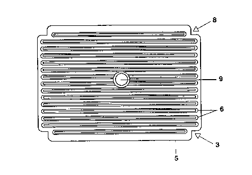
Fig. 1 shows an approximately rectangular inlay mat 3
with a length of 11 cm, a width of 7.5 cm and a total
thickness of 4.5 mm. Mutually parallel, longitudinally
oriented lamellae 6 of rectangular cross section with a
height of 2.5 mm and a width of approximately 1 mm are
arranged on the top side, which faces toward the heat
source, on a base body 5 with a thickness of 2 mm. The
underside 4 is smooth and thus provides optimum thermal
contact with the appliance wall. The lamellae 6 are
spaced apart by approximately 3 mm in each case. The
CA 02281469 1999-09-08
- 6 -
overall result is a structure with a sawtooth or
meandering cross section (Figure lc). The mat 3 has
indents 8 at its four corners and also a central hole
9, which together make it easier to hold and align the
mat 3 in the appliance or form recesses for attachment
means. The mat comprises modified hydrocarbon resin
which makes the mat sticky at its surface. The Shore A
hardness is 10. The mat therefore has good adhesion to
the base plate and very good thermal contact with the
circuit board.
An additional film 7 (cf. Figures 2 and 3) made from
plastic (Hostafen), which is arranged between mat and
base plate, makes it possible to ensure electrical
insulation between circuit board and base part even in
the unlikely event of a component penetrating through '
the mat or of current being fed through the mat to the
wall of the appliance. If the thickness of the film 7
is 0.1 mm, the result, in the installed state, is
therefore an overall thickness of 4.6 mm.
Figure 2 shows an operating device for a high-pressure
discharge lamp as an exemplary embodiment of an
electronic appliance. For this device, an electronic
ballast 10 is used with a housing made from plastic and
metal. This housing is divided into a metal base plate
12 made from aluminum and a top part 11 made from
plastic, comprising a cover 13 with attached side walls
14. A horizontal electronic circuit board 15 (shaded),
which is surrounded by the housing and on which the
electronic components (not shown) are mounted, is
attached to the base plate 12 by means of screws 20. In
addition, an on-edge circuit board (not visible) is
mounted in the interior 25 of the housing. An inlay mat
3 with good thermal conductivity is laid between
circuit board 15 and base plate 12. On one of the side
walls, there is a connection part 16 which is screwed
to the base plate 12 and is used for electrically
CA 02281469 1999-09-08
_ 7 _
connecting the lamp to the operating device and to
supply the operating device with voltage.
After the mounting circuit board 15, including the
electronic and electrical components which are arranged
thereon, has been attached to the base plate 12, the ,
top part 11 is fitted onto the base plate 12 and is
locked to the circuit board 15 by means of a
snap-action connection 18. The dimensions of the mat 3
are slightly smaller than those of the circuit board
15, so that there is no need to provide a special
recess on the mat 3 for the snap-action mechanism which
is located at the outer edge of the circuit board.
Fig. 3 shows the electronic ballast without the
surrounding cover or side wall. In addition to the
horizontal circuit board 15, the electronic ballast
also has a circuit board 17 which is positioned on
edge. The distance between the horizontal circuit board
15 and the base plate 12 is 4.5 mm. In this way, it is
ensured that the inlay mat 3 is always in thermally
conductive contact both with the circuit board 15 and
with the base plate 12.
The geometry of the mat is adapted to the geometry of
the base plate. A further mat of this nature may also
be inserted between the on-edge circuit board 17 and
the adjoining side wall.
A comparison with an identical operating device which,
however, was provided with conventional potting
compound revealed a considerable improvement in the
maximum permissible ambient temperature for the
luminaire of 15°C. While previous luminaires were only
able to tolerate an ambient temperature of 25°C, they
are now able to withstand a load of up to 40°C.