Note: Descriptions are shown in the official language in which they were submitted.
CA 02281666 1999-08-17
SPECIFICATION
IONTOPHORESIS DEVICE STRUCTURE
Technical Field
The present invention relates to an iontophoresis device
structure used for transdermal or transmucosal drug
administration.
Background Art
Much active research in recent years has been devoted to
preparations for transdermal or transmucosal administration,
because of the advantages of absorption of drugs through the
skin or mucous membranes of mammals, particularly humans, as
compared with oral administration, from the viewpoint of easier
administration, maintenance of blood levels and the ability
to avoid side effects of drugs in the alimentary tract.
Iontophoresis is one area which has received much attention
as an effective method for local administration which
accelerates absorption of drugs through the skin or mucous
membranes.
Iontophoresis is a type of method for accelerating physical
absorption of drugs whereby a voltage is applied to the skin
or mucous membrane to induce electrical migration of the drug,
for administration of the drug through the skin or mucous
membrane.
1
CA 02281666 1999-08-17
Iontophoresis apparatuses consist largely of a power
source apparatus which generates a current, and an
iontophoresis device structure which includes an electrode
layer for attachment to the skin or mucous membrane. Normally,
an iontophoresis device structure is separated into a donor
electrode which includes the drug, and a reference electrode.
The iontophoresis which delivers the drug through the skin or
mucous membrane is accomplished by forming a single electrical
circuit with the power source, the iontophoresis device
structure and the body and running a current through this
circuit for electrical driving.
Connection between the electrode layer of the
iontophoresis device structure and the power source is achieved
using a snap-type protruding terminal such as disclosed in
Japanese Laid-open Patent Publication No. 504343 of 1991 or
Japanese Laid-open Patent Publication No. 196644 of 1996.
A conventional iontophoresis device structure will now be
explained with reference to the attached drawings.
Fig. 7 is a cross-sectional schematic view of a
conventional iontophoresis device structure, and Fig. 8 is a
cross-sectional schematic view of another conventional
iontophoresis device structure.
Here, 20 is the conventional iontophoresis device
z
CA 02281666 1999-08-17
structure, 21 is a support formed into a cup shape, 22 is an
electrolyte layer fitted into the concave part of the support
21, 23 and 24 are snap-type protruding terminals, 25 is an
electrode layer electrically connected to the protruding
terminal 24, and 26 is a separator laminated in a freely
releasable manner on the rim around the opening of the concave
part of the support 21.
The method of electrification for the above-mentioned
iontophoresis device structure having this construction will
now be explained.
In the structure illustrated in Fig. 7, the flat section
under the protruding terminal 23 is contacted with the
electrolyte layer 22 for use as the electrode layer, and the
protruding part is connected with an external power source for
electrification.
In the structure illustrated in Fig. 8, the bottom surface
of the protruding terminal 24 is contacted with a separately
provided electrode layer 25 for electrical connection, and the
protruding part is connected with an external electrode for
electrification through the electrode layer 25 which has a wide
area.
These conventional iontophoresis device structures have
had the following problems, however. Specifically,
3
CA 02281666 1999-08-17
(1) An insertion hole must be formed for the protruding
terminal in order to project its protruding part through the
bottom of the concave part of the cup-shaped support and an
anchoring ring called a collar must be fitted to anchor the
protruding terminal, thus requiring more working steps and
reducing productivity, complicating mass production and
raising costs.
(2) Leakage of the electrolyte or solvent such as water
in the electrolyte layer from the insertion hole impairs the
quality and lowers product yields.
( 3 ) Because a non-flexible convex terminal is used as the
snap-type protruding terminal, when the area of the underside
of the terminal is widened to increase the contact between the
convex terminal and the electrolyte layer in the case of the
structure shown in Fig. 7, the contouring is poorer upon
attachment to the body, while conversely if the underside of
the terminal is reduced, a current flows directly under the
lower end of the terminal, resulting in greater danger of
electrical irritation to the body and lower safety.
(4) When a separate electrode layer is provided as shown
in Fig. 8, it is necessary to carry out an integrating step
for the more complex convex terminal as well as for the
electrode layer, and thus working efficiency is reduced,
4
CA 02281666 1999-08-17
productivity is impeded, and costs are increased.
(5) Although some structures employ silver or silver
chloride in an ABS resin as the material for the convex terminal,
and other structures have nickel platings on zinc, when ABS
resins are used the terminal must be formed to a prescribed
thickness to provide strength for the convex terminal, and
hence there is a limit to how thin the thickness of the lower
end of the terminal can be made. Also, structures wherein zinc
is covered with a nickel plating, etc., have the problem of
elution of the zinc or nickel, etc. , by the electrolyte reaction
upon electrification, so that the safety is poorer.
(6) When the protruding terminal is connected with the
external power source, excessive pressure on the protruding
terminal may break the iontophoresis device structure and cause
leakage of its contents, such as the electrolyte layer.
(7) Because the rim of the protruding terminal is round,
the connector is prone to detachment during electrification
by the external power source.
The present invention overcomes these problems by
providing an iontophoresis device structure which has
excellent contouring ability at its site of attachment, has
very high safety, is of high quality with high product yields,
and can be produced with fewer production steps to improve
CA 02281666 2001-10-30
working efficiency and increase productivity, to allow mass
production at low cost.
Disclosure of the Invention
- In order to achieve the object stated above, the present
invention has the following construction.
The iontophoresis device structure according to claim 1
of the invention has a construction provided with a cup-shaped
support including a concave part, at least one electrification
hole formed in the concave part, an electrode layer formed on
the flat part of the rim of the concave part, and an electrolyte
layer fitted into the concave part.
Since the electrode layer is anchored on the outside of
.the flat part of the rim around the concave part of the support
in this construction, its production is more simple allowing
notable improvement in working efficiency, increasing
productivity and lowering the cost. In addition, the adhesion
between the flat part of the rim around the concave part and
the electrode layer can be markedly
increased, to help prevent leakage of the solvent of the
electrolyte layer, etc.
Here, the support serves to hold the electrolyte layer,
and it may be any material with excellent workability,
flexibility and suitable shape retention and water retention;
6
CA 0228'1666 1999-08-17
as examples there may be mentioned chlorinated resins such as
vinylidene chloride and vinyl chloride polymers, as well as
olefin-based, ester-based, styrene-based, acrylic-based,
amide-based, oxymethylene-based, phenylene sulfide-based,
amidoimide-based, acrylonitrile-based, etherketone,
ethersulfone, sulfone, etherimide, butadiene and isoprene
high molecular polymers or their copolymers, though there is
no restriction to these and it is only necessary that the
material have the effect mentioned above. Materials which
have been formed into films and worked, or molded products,
may be used. The thickness is not particularly restricted,
but a thickness of 5-250 ,um is preferred for superior shape
retention and flexibility.
The electrolyte layer is a conductive layer containing an
electrolyte which supplies the body with a current from the
power source when directly contacted with human skin or a mucous
membrane, and it is preferred to use a nonwoven fabric
impregnated with an electrolyte solution, or an electrolyte
solution which has been gelled with a polysaccharide such as
agar or gelled using a synthetic polymer.
The iontophoresis device structure according to claim 2
of the invention has the construction of claim 1 wherein the
electrode layer is provided with an electrode layer base formed
CA 02281666 1999-08-17
of a film or sheet of a thermoplastic synthetic resin, and a
conductive layer formed on one side of the electrode layer base.
In this construction, theflexible electrode layer matches
the soft support and can therefore follow the shape of the site
of attachment. Also, since the electrode layer is made of an
easily moldable synthetic resin, the number of production steps
can be reduced to increase productivity.
The electrode layer base is a base sheet with a conductive
layer on the bottom side, and its shape is not limited to
circular but may be elliptical, square or rectangular; the
electrode terminal may likewise have any desired shape, and
if necessary a connector-anchoring cavity may be formed in the
terminal for more stable anchoring with the connector, etc.
The material used for the electrode layer base may be the
same material as the support. It is preferred to use an
identical synthetic resin as the support in order to allow
intimate heat sealing. Different types of synthetic resins
may also be used depending on the position and material of the
conductive layer.
The material used for the conductive layer may be metal
foil, carbon foil or the like, but preferably a conductive ink
paste is directly printed on a polymer sheet . As examples of
such conductive ink paste materials there may be mentioned
s
CA 02281666 1999-08-17
polarized electrode materials such as resin paints comprising
mixtures of carbon powder or graphite powder, non-polarized
materials such as silver- or copper-based materials for the
anode and resin materials comprising silver/silver chloride,
copper/copper chloride mixtures for the cathode; however,
non-polarized materials which do not produce foaming under pH
changes or electrolysis of water are particularly preferred
for use.
The iontophoresis device structure according to claim 3
of the invention has the construction of claim 1 or 2 wherein
the electrode layer is laid onto the flat part via an adhesive
layer.
According to this construction, the electrode layer may
be anchored to the surface of the flat part by simple adhesion
with an adhesive agent, and since it is adhered on the outside
of the support it is possible to prevent coating leakage of
the adhesive agent and ensure anchorage of the electrode layer.
Because the electrode layer and the cup-shaped support are
thoroughly bonded, leakage and escape of the contents can be
reliably prevented. The flexibility of the structure as a
whole provides a better feel during use and makes it easier
to design a line for mass production.
The iontophoresis device structure according to claim 4
9
CA 02281666 1999-08-17
of the invention has the construction of claim 3 wherein the
adhesive agent of the adhesive layer is of one or more types
from among acrylic-based, silicon-based or rubber-based
pressure sensitive adhesive agents and heat sealing agents such
as polyolefins or their esters.
According to this construction, the adhesive agent used
is one which is commonly used, such as a pressure-sensitive
adhesive agent which is an acrylic-based agent with high
adhesive strength, a silicon-based agent which is resistant
to corrosion in gel contents or an inexpensive rubber-based
agent, or a heat sealing agent made of a polyolefin or its ester.
These may be appropriately selected depending on the size and
the purpose of use of the iontophoresis device structure. The
adhesive agent accomplishes thorough sealing between the
electrode layer and the flat part of the support, for a tight
sealing effect.
When heat sealing is carried out for adhesion between the
electrode layer and the cup, the heat sealing temperature will
depend on the melting point of the aforementioned polymer film,
but will generally be 100-250 °C, and preferably 120-200 °C.
As the heat sealing temperature increases above 200 °C, cracks
will tend to be produced in the electrode layer, while as it
decreases below 120 °C more time will be required for the heat
to
CA 02281666 1999-08-17
sealing, which will tend to lower working efficiency, and
therefore neither extreme is preferred.
The iontophoresis device structure according to claim 5
of the invention has the construction according to any one of
claims 1 through 4, wherein the electrode layer has an
electrification connecting member from the external power
source, and the connecting member is a projection formed as
a bulge from the rim of the electrode layer, or a recess formed
parallel to the direction of height of the rim of the concave
part of the support and the exposed part of the electrode layer
which is exposed at the recess.
According to this construction, connection with the
external power source for administration of the preparation
can be simplified because of the projection provided.
Here, the size of the projection or exposed electrode layer
as the connecting member may be a sufficient size or length
to allow electrical connection with different types of
connectors, and in order to prevent misconnection with the
connector, a connector latch with a thickened end may be
provided. A connection hole for the connector may also be
opened in the projection or exposed electrode layer.
Brief Description of the Drawings
11
CA 02281666 2001-10-30
Fig. 1 is a plan view of an iontophoresis device structure
according to a first embodiment of the invention.
Fig. 2 is a perspective view of the support of an
iontophoresis device structure according to the first
embodiment of the invention.
Fig. 3 is a perspective view of the electrode layer of the
iontophoresis device structure according to the first
embodiment of the invention.
Fig. 4 is a cross-sectional view showing major parts of
the assembly of the iontophoresis device structure according
to the first embodiment of the invention.
Fig. 5 (a) to (e) are a series of sketches showing the
production steps for the iontophoresis device structure
~according'to the first embodiment of the invention.
Fig. 6(a) is a perspective view of an iontophoresis device
structure according to a second embodiment of the invention.
Fig. 6(b} is a plan view of the iontophoresis device
structure according to the second embodiment of the invention.
Fig. 6 (c ) is a plan view of the support of the iontophoresis
device structure according to the second embodiment of the
invention.
Fig. 7 is a cross-sectional schematic view of a
conventional iontophoresis device structure. (prior art)
12
CA 02281666 2001-10-30
Fig. 8 is a cross-sectional schematic view of another
conventional iontophoresis device structure. (prior art)
Best Mode for Carrying Out the Invention
Embodiments of the present invention will now be explained
with reference to the drawings.
(First embodiment)
Fig. 1 is a plan view of an iontophoresis device structure
according to the first embodiment of the invention, Fig. 2 is
a perspective view of its support, Fig. 3 is a perspective view
of its electrode layer and Fig. 4 is a cross-sectional view
showing major parts of its assembly.
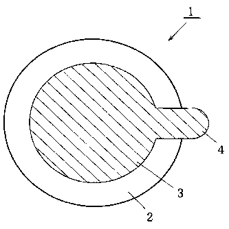
In Figs. 1 and 2, 1 is the iontophoresis device structure
according~to this embodiment, 2 is the support formed into a
cup shape from a thermoplastic resin such as polyethylene
terephthalate, 3 is the electrode layer, 4 is the projection
formed as a partial extension of the electrode layer 3, and
is an electrification hole formed as a single opening in the
bottom of the concave part of the support 2. In Fig. 3, the
electrode layer 3 is formed of an electrode layer base 3a and
a conductive layer 3b, the electrode layer base 3a being formed
of a polyethylene terephthalate film and the conductive layer
3b being formed by printing of conductive silver paste ink
13
CA 02281666 1999-08-17
(product name: Achison ED6022 by Nihon Achison) on the surface
of the electrode layer base 3a to a dry thickness of about 20
,(.Cm. In Fig. 4, 6 is an electrolyte layer made of a gel or the
like packed into the concave part of the support 2.
The support 2 here is formed into a circular shape, but
it may also be elliptical or rectangular. Also, only one
electrification hole 5 was formed in the support 2, but 2 or
more holes, or a mesh, may also be formed.
A process for fabricating the iontophoresis device
structure of this embodiment having the construction described
above will now be explained with reference to the drawings.
Fig. 5 is a series of sketches showing the production steps
for the iontophoresis device structure of this embodiment.
In the drawings, 10 is an electrode layer base-forming
material made of a polyethylene terephthalate or other
thermoplastic synthetic resin film or sheet with a thickness
of 100 ,u m, 11 is a conductive layer formed by printing of
conductive silver paste ink (product name: Achison ED6022 by
Nihon Achison) on the electrode layer base-forming material
to a dry thickness of about 20 ,(.tm, 12 is an adhesive layer
made of a heat sealing agent or pressure sensitive adhesive
agent applied around the rim of the conductive layer 11, and
13 is the flat part of the support 2.
14
CA 02281666 1999-08-17
The fabrication process involves first printing thesilver
paste ink on the electrode layer base-forming material 10 as
shown in (a) to form the conductive layer 11 (conductive
layer-forming step) , and then coating the rim of the conductive
layer 11 with a heat sealing agent or pressure sensitive
adhesive agent to about the same width as the flat part 13 of
the support 2 as shown in (b), to make the adhesive layer 12
(adhesive layer-forming step). Next, the electrode layer
base-forming material 10 is cut out leaving the electrode layer
3 and a projection 4 as shown in (c) (cutting step). The
adhesive layer 12 is then laid onto the flat part 13 of the
separately formed support 2 as shown in (d) and heat sealed
to obtain the iontophoresis device structure.
(Second embodiment)
Fig. 6 ( a ) is a perspective view of an iontophoresis device
structure according to a second embodiment of the invention,
Fig . 6 ( b ) is a plan view thereof , and Fig . 6 ( c ) is a plan view
of its support.
In the drawings, la is the iontophoresis device structure
of the second embodiment, 2a is the support, 3a is the electrode
layer formed into a circle, 4a is the exposed electrode layer
as one of the connecting members, 5a indicates electrification
holes formed at 3 locations on the flat part 13, and 14 is a
CA 02281666 1999-08-17
recess formed parallel to the direction of height of the concave
part of the support 2a.
According to this embodiment, the recess 14 under the
exposed electrode layer 4a allows easier connection with a
connector. An additional effect is that if a separator is
sealed to the support after the electrolyte layer or other
contents have been packed into the concave part, sealing is
thus facilitated since no protruding projection is present.
Industrial Applicability
As explained above, the present invention makes it possible
to realize an iontophoresis device structure which provides
the following excellent effects.
(a) Escape and leakage of the contents can be reliably
prevented by simple attachment of the electrode layer to the
cup-shaped support which holds the electrolyte, to obtain a
very high quality iontophoresis device structure.
(b) Because the entire structure is flexible, it easily
follows the shape of the site of attachment, so that it may
be attached without causing discomfort.
(c) Since very few production steps are necessary, mass
production is possible at low cost.
( d ) The connecting member allows connection with a power
16
CA 02281666 1999-08-17
source to be accomplished very easily and reliably.
(e) Since no hard protruding terminal is present, it is
easy to house the structure during transport and storage.
1~