Note: Descriptions are shown in the official language in which they were submitted.
CA 02282423 1999-09-02
WO 98139686 PCT/SE98/00067-
OPTICAL DEVICE
Technical Field
The present invention relates to an optical wavelength selective device, and
more
specifically to a wavelength selective switch for redirecting wavelength
channels in
an optical network, where each wavelength channel may be redirected
individually.
The invention also comprises a method for switching or add/drop multiplexing
of
wavelength channels in an optical network.
State of the Art
A number of different methods are known to further increase the capacity in
existing
optical networks. One way is to use so called wavelength division multiplexing
(WDM) technology to improve the degree of utilization of the available
bandwidth
on an optical fibre in the optical network. To increase the flexibility of the
network,
devices that can perform the redirection of traffic in the optical network are
needed.
The forementioned devices for the redirection of traffic can also help in
using the
network as efficiently as possible, and in case of a break in the network.
In "Wavelength Division Multiplexer with Photoinduced Bragg Gratings
Fabricated
in a Planar Lightwave Circuit Type Asymmetric Mach Zehnder interferometer on
Si", Y. Hibino et. al., an optical element is described in which Bragg grating
and
phase control elements are used in a Mach Zehnder interferometer. The intended
applications are wavelength division multiplexing and wavelength division
demultiplexing.
The apparatus mentioned above however cannot be used as a wavelength selective
switch. If the above mentioned apparatus is to be used for add/drop of several
channels the same number of apparatuses as the number of handled add/drop
pairs
CA 02282423 1999-09-02
WO 98/39686 PCT/SE98I00067
2
are needed. This type of apparatus is relatively difficult to reconfigure,
that is, it is
inflexible.
One problem with wavelength selective switches according to the prior art is
that
they require very big and complicated structures or several components, which
results in large power losses and high costs.
Summary of the Invention
A number of known methods can be used to increase the capacity in an optical
transmission system. In e.g. wavelength division multiplexing transmission
channels
are multiplexed and demultiplexed on different carrier wavelengths onto, resp.
out
from, an information flow. This multiplexing and demultiplexing requires
optically
wavelength selective devices. It may also be desirable to change the route of
transmission through the optical network for certain wavelength channels. For
this
purpose components with wavelength selective properties are required, for
example
in the form of a wavelength selective switch.
One problem with known wavelength selective switches is that they contribute
to
large power losses.
Another problem is that known wavelength selective switches have a relatively
complex structure and, in all the cases known to us, a relatively large number
of
different components.
A further problem is that known wavelength selective switches are relatively
expensive to manufacture because of the above mentioned complex structure and
the
large number of components.
CA 02282423 1999-09-02
WO 98/39686 PCT/SE98/00067
3
The present invention approaches the above mentioned problems by a wavelength
selective switch comprising at least one MMI (Mufti Mode Interference)
structure, at
least one Bragg grating, at least one Mach Zehnder waveguide and at least one
phase
control element.
The above mentioned MMI structure is used for splitting up light. The
distribution of
light intensity at one of the inputs of the MMI structure is depicted on all
outlets of
the MMI structure when its length is selected correctly. A deeper theory
behind this
is found in L.B. Soldano and E.C.M. Pennings, "Optical Mufti Mode Interference
Devices Based on Self Imaging: Principles and Application", J. Lightwave
Technology. Vol. 13(4), pp 615-627, 1995.
A Bragg grating is used filtering light. Filtering means that certain
wavelengths are
allowed to pass while other are reflected. The Bragg grating can be said to
constitute
a kind of wavelength selective mirror. Said reflection of certain wavelengths
can be
achieved in a number of ways; common to most of these methods is that the
reflection is achieved by periodically changing the index of the substance in
the
waveguide.
The above mentioned phase control element is needed for certain switching
functions and for the correction of process imperfections. There are several
types of
phase control elements; fundamental for all of them however is that the
optical
wavelength is affected through an applied external signal (voltage, current,
light or
heat). Usually a so called thermo-optical element is used, that is, the
refractive index
and thereby the wavelength, is affected by means of heat.
The wavelength selective switch according to the invention may comprise MMI
waveguides at both its connection sides. Said MMI waveguides can on their free
sides comprise a number of inputs consisting, for example, of so called access
CA 02282423 1999-09-02
WO 98/39686 PCTlSE98/00067
4 ..
waveguides for optical signals. Between said MMI waveguides a number of Mach
Zehnder waveguides are arranged. These Mach Zehnder waveguides in turn
comprise a number of phase control elements and a number of Bragg gratings.
The
number of phase control elements may be one more than the number of Bragg
gratings in the cases when one only wants to control any transmitted
wavelength
channels. In the case when only reflected wavelength channels are of interest,
the
number of phase control elements and Bragg gratings may be the same. The
number
of Bragg gratings and phase control elements may be equivalent for each Mach
Zehnder waveguide. Each Mach Zehnder waveguide comprising said phase control
elements and Bragg gratings may be identical.
By adjusting the shape and the dimension of the MMI waveguide and the length
of
the Mach Zehnder waveguides one can, by means of suitable phase control
elements
direct an optical signal from an input on the first MMI waveguide to an
arbitrary
output on the second MMI waveguide.
The object of the present invention is to achieve a wavelength selective
switch which
by its structure is as simple and as compact as possible so that the
manufacturing
cost may thus be reduced compared to the prior art technology.
An advantage of the present invention is that the power loss may be kept
relatively
low.
Another advantage of the present invention is that its performance in other
areas
such as crosstalk and the Iike may be improved compared to prior art.
The invention will now be described in more detail by means of preferred
embodiments and with reference to the enclosed drawings.
CA 02282423 1999-09-02
WO 98/39686 PCT/SE98/0006'~
Brief Description of the Drawings
Figure 1 shows an embodiment of a wavelength selective switch according to the
invention.
Figure 2 shows a second embodiment of a wavelength selective switch according
to
the invention.
Description of Preferred Embodiments
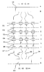
In figure 1 a wavelength selective switch according to the invention is shown.
The
support lines A-K show sections used to describe the invention. In this
embodiment
the wavelength selective switch can handle four different wavelengths
independently
of each other. At the first connection end of the wavelength selective switch
a first
MMI waveguide is arranged and at the other connection end of the wavelength
selective switch a second MMI waveguide 20 is arranged. The first MMI
waveguide
in this embodiment comprises one or more access waveguides 11, 12, 13, 14 and
the second MMI waveguide 20 comprises one or more access waveguides 21, 22,
23,
24. Between the first MMI waveguide 10 and the second MMI waveguide 20 four so
called Mach Zehnder waveguides 31, 32, 33, 34 are arranged. Each of the above
mentioned Mach Zehnder waveguides comprises four phase control elements 51,
53,
55, 57 and three Bragg gratings 62, 64, 66.
The above mentioned wavelength selective switch of course may be upgraded to
comprise N wavelength channels instead of the four wavelength channels shown
in
the above mentioned embodiment. Generally however, in order for the wavelength
selective switch to be able to handle N wavelength channels independently of
each
other, it must comprise Nx(N-1 ) Bragg gratings, N2 phase control elements and
N
access waveguides, each arranged in connection to an MMI waveguide.
CA 02282423 1999-09-02
WO 98/39686 PCT/SE98100067
6 -.
Suppose that light is excited onto the access waveguide 11 belonging to the
MMI
waveguide 10 at section A. The length of the MMI waveguide 10 is selected so
that
N images of the light intensity from the access waveguide 11 at section A are
achieved in the MMI waveguide 10 along section B. Next suppose that the
structure
and dimensions of the MMI waveguide 10 have been selected so that four images,
that is N=4, of the original distribution in the access waveguide are
achieved. If the
access waveguides 11, 12, 13, 14 have been arranged at the MMI waveguide 10 in
a
correct way, that is, if they have been positioned correctly, and if the cross-
sectional
dimension and positioning of the Mach Zehnder arms 31, 32, 33, 34 have been
chosen correctly, a large fraction of the energy in the images will be
connected to the
Mach Zehnder waveguides 31, 32, 33, 34. The maximum energy of these images is
<1/N of the energy along section A if perfect uniformity is achieved, that is,
in this
case <1/4 of the energy along section A. This intensity distribution will
differ very
little if light is instead excited from any of the access waveguides 12-14
along
section A.
In contrast, the phase relationship is strongly dependent on the access
waveguide at
which light is excited into the MMI waveguide. This input access waveguide
dependent phase relationship is the key to the functionality of the component.
Because of reciprocity, light with the corresponding phase relationship at
section B
travelling in the reverse direction, that is, from the bottom upwards
according to
figure 1, will be focused on the corresponding access waveguides.
Sections along the support lines D, F and H denote Bragg grating sections. The
Bragg gratings along each support line may be identical. If they are identical
the
grating sections will reflect the wavelength along the corresponding support
line for
each of the Mach Zehnder waveguides 31, 32, 33, 34. The wavelengths that are
reflected return to the MMI 10 with the phase relationship determined by the
phase
control elements 51, 53, 55.
CA 02282423 1999-09-02
WO 98/39686 PCT/SE98/0006'F
7
Suppose, for example, that the Bragg gratings along section D reflect a
wavelength
~,1, and the Bragg gratings along section F reflect a wavelength a,2; the
phase control
elements 51 along section C will then determine which access waveguide 11-14
will
be the output for the wavelength ~.2. The analogous situation is seen along
section G,
that is, the phase control element 55 along said section G determine which one
of the
access waveguides 11-14 will be the output for the wavelength ~,3, which has
been
reflected by the Bragg gratings along section H.
The phase relationship onto the MMI waveguide 10 in the reverse direction can
thus
be selected individually for each wavelength, that is, each wavelength channel
can
be assigned an output independently of other wavelength channels. This of
course
implies that, for example, the phase control element 53 along section E can
compensate for the phase control element 51 along section C and that the phase
control element 55 along section G can compensate for the phase control
elements
51, 53 along sections C and E respectively, and that the phase control element
57
along section I can compensate for the phase control elements 51, 53, 55 along
the
sections C, E and G respectively. In general, each phase control element must
be
able to compensate for the phase control elements arranged before it in the
transmission route of the channels along the same Mach Zehnder waveguide.
Of course the phase control element 51 along the support line C also affects
the
wavelength channels ~,2, ~,3 and ~,4. This compensation can, however, easily
be
software controlled according to teachings known to a person skilled in the
art, and,
therefore, will not be described in detail here. There is also the
possibility, if said
compensation is not desired to be software controlled, to extend the phase
control
elements 51, 53, 55, 57 successively from section C in the direction towards
section
I in a suitable manner.
CA 02282423 1999-09-02
WO 98139686 PCT/SE98/00067
8
The wavelength channel or channels not reflected by a Bragg grating will reach
the
MMI 20 and the phase relationship along support line J will determine to which
output along support line K the respective wavelength channel is excited. If
length of
the Mach Zehnder waveguides 31, 32, 33, 34 are equivalent the wave length
channels that reach the MMI 20 will be focused on the same output. The
difference
in length between the Mach Zehnder waveguides 31, 32, 33, 34 can also be
selected
so that different wavelengths that reach the MMI 10 are focused on different
access
waveguides 21, 22, 23, 24 along the support line K.
In figure 2 another embodiment of a wavelength selective switch according to
the
invention is shown. The support lines A-H show sections used to describe the
invention. This embodiment comprises an MMI waveguide 10 and four Mach
Zehnder waveguides 31, 32, 33, 34. On one side of the MMI waveguide 10 four
access waveguides 11, 12, 13, 14 are arranged. On the opposite side relative
to said
access waveguides, said Mach Zehnder waveguides 31, 32, 33, 34 are arranged.
On
each of these Mach Zehnder waveguides 31, 32, 33, 34 three Bragg gratings 62,
64,
66 and three phase control elements 51, 53, 55 are arranged.
Suppose that a wavelength channel is sent to an access waveguide 11 arranged
on
the MMI waveguide 10. This wavelength channel passes through the MMI
waveguide. The length and the structure of the MMI waveguide are selected so
that
N images of the light intensity from the access waveguide 11 at section A are
achieved in the MMI waveguide along section B. In this case, suppose that the
length and the structure have been selected so that four images are achieved.
If the
access waveguides 11, 12, 13, I4 have been arranged at the MMI waveguide 10 in
a
correct way, that is, if they have been positioned correctly, and if the cross-
sectional
dimension and positioning of the Mach Zehnder waveguides 31, 32, 33, 34 have
been chosen correctly, a large fraction of the energy in the images will be
connected
to the Mach Zehnder waveguides 31, 32, 33, 34. The maximum energy for these
CA 02282423 1999-09-02
WO 98/39686 PCT/SE98/00067
9
images is < 1 /N of the energy along section A if perfect uniformity is
achieved, that
is, in this case <1/4 of the energy along section A. This intensity
distribution will
differ very little if light is instead excited from any of the access
waveguides 12-14
along section A.
The phase relationships on the other hand depend strongly on at which of the
access
waveguides light is excited onto the MMI waveguide. This input access
waveguide
dependent phase relation is the key to the functionality of the component.
Because of
reciprocity, light with the corresponding phase relationship at section B
travelling in
the reverse direction, that is from the bottom upwards according to figure 2,
will be
focused on the corresponding access waveguide.
Sections along the support lines D, F and H denote Bragg grating sections. The
Bragg gratings along each support line may be identical. If they are identical
the
grating sections will reflect the wavelength along the corresponding support
line for
each of the Mach Zehnder waveguides 31, 32, 33, 34. The wavelengths which are
reflected return to the MMI 10 with the phase relationship determined by the
phase
control elements 51, 53, 55.
Suppose, for example, that the Bragg gratings along section D reflect the
wavelength
~.1, and that the Bragg gratings along section F reflect the wavelength ~.2;
then the
phase control elements 51 along section C will determine which access
waveguide
11-14 will be the output of, for example, a wavelength ~,1, the phase control
elements 53 along section E will determine which access waveguide 11-14 will
be
the output of, for example, a wavelength ~,2. The analogous situation is seen
along
section G, that is, the relevant phase control element 55 along said section
will
determine which one of the access waveguides 11-14 will be the output of the
wavelength ~.3, which has been reflected by the Bragg gratings along section
H.
CA 02282423 1999-09-02
WO 98/39686 PCT/SE98/00067
The phase relationship onto the MMI waveguide 10 in the reverse direction may
thus
be selected individually for each wavelength, that is, each wavelength channel
may
be assigned an output independently of other wavelength channels. This of
course
implies that, for example, the phase control element 53 along section E can
compensate for the phase control element 51 along section C and that the phase
control element 53 along section G can compensate for the phase control
elements
51, 53 along sections C and E respectively. In general each phase control
element is
to be able to compensate for the phase control elements arranged before it in
the
transmission path of the channels along the same Mach Zehnder waveguide.
It is of course also the case that the phase control element 5 i along the
support line
C also affects the wavelength channels ~.2, ~.3 and ~,4. This compensation
can,
however, easily be software controlled according to theories well known to the
person skilled in the art, and thus will not need to be described in more
detail here.
There is also the possibility, if said compensation is not desired to be
software
controlled, to extend the phase control elements 51, 53, SS from section C in
the
direction towards section G successively in a suitable manner.
The wavelength channel or channels which are not reflected by any Bragg
grating
will be excited from the relevant Mach Zehnder waveguide 31, 32, 33, 34.
The materials that may be suitable for manufacturing of the present invention
are, for
example, quartz (Si02), polymers, lithium niobate (LiNb03) or a semiconductor
system.
The invention is of course not limited to the embodiments described above and
shown in the drawings, but may be modified within the scope of the appended
patent
claims.