Note: Descriptions are shown in the official language in which they were submitted.
- CA 02282610 1999-09-16
10-198 CA
IMPROVED POWER TAP
The invention pertains to an optical waveguide structure, such as a switch or
a
Mach-Zehnder Interferometer (MZI), which comprises at least one optical main
waveguide and at least one power tap.
Due to the increasing use of optical fibre communication channels, the
development of optical devices for direct processing of optical signals has
become of significant importance to system designers. One particularly useful
1o approach to optical processing is through the use of integrated waveguide
structures formed on, e.g., silicon substrates. The basic structure of such
devices is known to those skilled in the art. Depending on the precise
configuration of the waveguide, such devices can perform a wide variety of
functions including tapping signal power from the optical waveguide. In a
typical
.tapping application of integrated optical devices, two waveguides pass in
close
adjacency for a certain length, i.e., coupler length, dependent upon the
desired
degree of coupling. Energy from one waveguide core is transferred to ~ an
adjacent core to effectuate the signal tap. One shortcoming of such optical
tap
configurations is that the tapped signal tends to be dependent upon the
2o wavelength and on polarization of the signal due to interterometric and/or
multi
mode effects.
U.S. Patent 5,539,850 describes an optical device for tapping signal power
wherein the signal tap provided is substantially independent of wavelength and
polarization. This is achieved by two tap means each selected to compensate
for the other's wavelength and polarization dependencies. The disclosed
structure thus renders tapping wavelength independent by comprising two taps.
Another approach to tapping of an optical signal is described in U.S. Patent
4,076,375, which discloses an optical waveguide coupler and power tap for use
with optical fibres or planar-form optical waveguides. Abutted to the end of
the
3o cladded optical transmission waveguide is a section of a second optical
CA 02282610 1999-09-16
10-198 CA
2
waveguide comprising a core surrounded by a cladding layer, the said core
having a smaller cross-sectional area than the core of the transmission
waveguide. By this arrangement, a significant amount of the core guided
modes in the direction of the transmission waveguide is coupled into the
s cladding layer of said second waveguide at the abutting point for tapping.
The present invention seeks to provide a tolerant optical waveguide structure
for tapping the power carried by the main optical waveguide mode that, on the
one hand, shows only a low power loss while tapping and little wavelength
dependence and, on the other hand, has a comparatively simple arrangement.
1o This is achieved by employing an optical waveguide structure as described
in
the first paragraph wherein the optical main waveguide gradually widens over a
length L~aPer to a width W,ape~ and then gradually narrows to a finite width,
thereby
forming a tapered waveguide, and the power tap branches from the tapered
waveguide.
15 Due to the tapered form of the main waveguide provided by the present
invention, the guided mode is forced to gradually widen up to the broad end of
the taper and then to gradually narrow again. By tapping at or near this broad
end of the taper using a power tap exhibiting, e.g., a cross-sectional area
comparable to that of the main waveguide before widening or even smaller,
20 only a fraction of the guided mode will be coupled into this power tap.
This
fraction depends on the overlap of the widened mode with the tap waveguide.
The arrangement provided by the present invention thus allows purely
geometrical properties control the tapped power, which can therefore easily be
kept low.
25 It is preferred that the optical main waveguide gradually narrows
substantially to
its original width.
It is also preferred that the power tap branches at or near W~ape~
CA 02282610 1999-09-16
3
10-198 CA
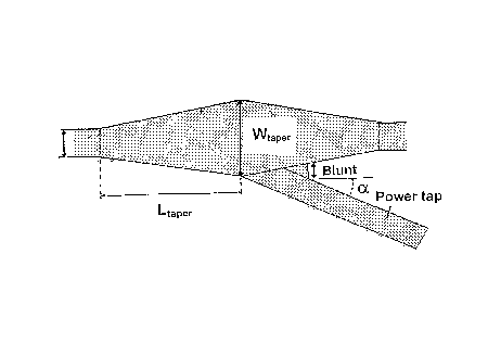
Referring to Fig. 1, shown is a schematic drawing of an optical waveguide
structure according to the present invention. It can be seen that the main
waveguide gradually widens from its original width over the taper length
L~aPer to
the Width W,aper, the broad end of the taper, and then gradually narrows
again.
The power tap is positioned near the broad end of the taper.
It is preferred that the W,aper is greater than about two times of the
original width
of the main waveguide.
It should be borne in mind that the terms "tapered waveguide" and "taper" as
used for the description of the main waveguide generally encompasses
1o geometric forms that gradually widen and narrow again, i.e. in a non-
straight
way, such as parabolic shapes, without the scope of the present invention
being exceeded. The form of the optical waveguide structure as shown in Fig. 1
thus is only one example of a tapered form.
A further advantage of the invention is that due to the fact that the fraction
of
~5 the guided mode that is coupled into the power tap depends on geometrical
properties and not on interference and/or multi mode effects, the tapping will
become virtually wavelength independent.
The optical waveguide structure according to the present invention has a
simple structure and can easily be manufactured by those skilled in the art.
2o Furthermore, since tapping is done at or near the broad end of the taper,
i.e. in
a rather insensitive location, the waveguide structure shows a good
manufacturing tolerance with regard to geometry and refraction index
variations.
Preferred in the present invention are planar optical waveguides.
2s It is noted that JP 56140305 A discloses an optical branching and coupling
circuit with an optical mixing waveguide in a tapered shape. The broadening of
the waveguide in JP 56140305 A results in less insertion loss and minimizes
uneven distribution. The fibre bundles that take up the light, however, are
CA 02282610 1999-09-16
10-198 CA
4
connected to the narrow ends of the mixing waveguides. Furthermore, JP
56140305 does not disclose a power tap.
It should be clear from the aforementioned that also the power tap itself will
usually be an optical waveguide. As tapping is mainly dependent on the
geometrical properties of the waveguide structure that comprises the tapered
waveguide and the power tap, the manufacture of the tapered waveguide and
the waveguide for the power tap can be performed in a similar way with respect
to the manufacturing steps and the employed materials, provided the necessary
geometrical arrangement is achieved.
1o The manufacture of optical waveguides is known in itself. Such waveguides
are
used in optical devices, which are commonly optical fibre-compatible. It is
preferred that the tapered waveguide and the power tap consist essentially of
embedded or embedded ridge-type channel waveguides which comprise a high
refractive index core component embedded in a lower refractive index cladding
component. The index contrast ~n between the high refractive index core and
the lower refractive index cladding required to keep the propagating mode in
the core of the waveguide is usually between 0.001 and 0.01.
The cladding component may be glass or a polymeric material. The core
component, which comprises the actual waveguide design, may be made of
2o inorganic or polymeric material.
Within the framework of the present invention, cladding and core components
of polymeric materials are preferred. The polymers used for these components
are so-called optical polymers. The refractive index of the optical polymers
used
will generally be within the range of from 1.4 to 1.8.
Optical polymers are known, and the person of ordinary skill in the art will
be
able to choose polymers having the appropriate refractive indices, or to adapt
the refractive indices of polymers by chemical modification, e.g., by
introducing
monomeric units that affect the refractive index.
CA 02282610 1999-09-16
10-198 CA
Suitable materials for and configurations of the cladding and core components
are disclosed, int. al., in M.B.J. Diemeer et al., "Polymeric phased array
wavelength multiplexer operating around 1550 nm," Electronics Letters, Vol. 32
(1996), pp. 1132-1133; and T.A. Tumolillo et al., "Solid State Optical Space
5 Switches for Network Cross-Connect and Protection Applications," IEEE
Communications Magazine (1997), pages 124-130; and International Patent
Application WO 97/01782.
Underneath the core and cladding components there usually is a support, e.g.,
a glass or silicon substrate, which latter is preferred.
It is preferred that the thickness of the optical waveguide does not change in
the course of gradual narrowing or widening.
The geometrical arrangements of the optical waveguide structure for an index
contrast On between core and cladding of smaller than 0.01 are described
hereinafter.
In a preferred embodiment, the taper length L~ape~as measured from the onset
of
widening to the broad end of the taper is greater than 0.1 mm and smaller than
10 mm, preferably between 4 mm and 8 mm.
In yet another preferred embodiment the broad end of the taper has a width
Wtaper of greater than 1 Nm and smaller than 100 Nm, preferably between 10 Nm
2o and 30 Nm.
The preferred dimensions of the taper allow sufficient widening of the
propagating mode at or near the point of tapping and thus lead to the desired
low power loss and wavelength independence.
It is a particular advantage of the present invention that the tapped fraction
can
be determined by adjusting the power tap relative to the tapered waveguide.
This adjustment can be described by a tap angle a that is defined as the angle
CA 02282610 1999-09-16
10-198 CA
6
between the center line of the tapered waveguide and the center line of the
power tap.
Referring to Fig. 1, there is also shown an example for the tap angle a.
In a preferred embodiment of the present invention the tap angle a is greater
than 0.1 degrees and smaller than 10 degrees, preferably between 1 and 5
degrees. By varying the tap angle a while designing the waveguide structure,
it
. is possible to set the power transferred during tapping.
Also referring to Fig. 1, it is shown that a blunt can be introduced between
the
tapered waveguide and the branching power tap. The blunt may be regarded
as an additional design parameter. By varying the blunt size it is also
possible
to optimize, e.g., the excess loss and the power transferred during tapping.
The
blunt size as measured along the broad end of the blunt between the tapered
waveguide and the branching power tap is greater than. 0.1 Nm and smaller
than 10 Nm, preferably between 0.5 Nm .and 2 Nm.
~5 In yet another preferred embodiment of the present invention the space
between the tapered waveguide and the power tap is bridged. Like a blunt, this
bridge, also an extra design parameter, serves to improve the isolation
between
the main waveguide and the power tap. Without this separating space there is
still a direct connection between the main waveguide and the branching power
2o tap. Referring to Fig. 2, it is shown that the separating space (Sep.)
between
the afore-mentioned two components enhances the isolation, which will further
reduce the power loss.
Of course this invention also pertains to active optical components, such as
1xN switches, switch matrices, and Mach-Zehnder-Interferometers, so-called
25 thermo-optical (TO) components, or electro-optical components (EO) that
comprise an optical waveguide structure according to the invention. Both
thermo-optical and electro-optical components are known.
CA 02282610 1999-09-16
10-198 CA
7
The working of thermo-optical components is based on the phenomenon of the
optical waveguide material employed exhibiting a temperature dependent
refractive index. On top of the upper cladding layer heating elements are
provided (usually metal strips) to heat the polymeric cladding and core
materials, in order to change the refractive index for switching.
The working of electro-optical devices is based on the phenomenon of the non
linear optically active material employed exhibiting an electric field
dependent
refractive index. On top of the upper cladding layer electrodes are provided
to
apply an electric field to the non-linear optically active material to change
the
1o refractive index for switching.
Of course, the invention also applies to passive optical components, like
splitters, (de)multiplexers, and combiners, that comprise an optical waveguide
structure according to the invention.
Active and passive optical components or devices can be used in optical
1s communications networks of various kinds. Generally, the optical components
either will be directly combined with optical components such as light sources
(laser diodes) or detectors, or they will be coupled to input and output
optical
fibres, usually glass fibres.
The invention will now be illustrated by way of the following unlimitative
2o examples.
Example 1
A waveguide structure according to the present invention comprising a power
tap and a tapered waveguide was manufactured showing the following
25 dimensions:
main waveguide width - 6 pm
power tap width - 6 Nm
.~ CA 02282610 1999-09-16
10-198 CA
8
~-taper - 6.0 mm
Wtaper - 16. 0 N m
tap angle a ~ - 2.25 degrees
blunt size - 0.8 Nm
refractive index contrast (fin) - 0.006
This waveguide structure showed at a wavelength of 1538 nm a tap ratio, which
is the percentage ratio of the power in the tap (power tap) to the power in
the
main waveguide (power main), of 4.5 %.
(tap ratio (%) = power tap/power main].
Example 2
A waveguide structure was manufactured according to Example 1, except that
now the tap angle a was varied from 3.5 to 1Ø Table 1 shows the results with
respect to the tap ratio.
Table 1
tap angle a tap ratio (%)
(degrees) (= power taplpower
main
x100)
3.5 2.0
2.25 4.5
1.5 7.3
1.0 16.9
2o It can be seen from the results of Table 1 that increasing the tap angle a
can
reduce the tap ratio at a wavelength of 1538 nm.
' CA 02282610 1999-09-16
10-198 CA
9
Example 3
A waveguide structure was manufactured according to Example 1, except that
now the wavelength was varied. Table 2 shows the results with respect to the
tap ratio.
Table 2
wavelength tap ratio (%)
(nm)
(= power tap/power
main
. x100)
1535 4.5
1545 4.6
1555 4.6
1560 4.7
It can be seen from the results of table 2 that the tap ratio remains rather
1o constant when varying the wavelength, showing that tapping of power in the
waveguide structure of the present invention is virtually wavelength
independent.