Note: Descriptions are shown in the official language in which they were submitted.
CA 02283088 1999-08-04
_ wo ~szs6 rcwrnUS~oo3is
ANALOG CIRCUIT FOR AN AUTOFOCUS MICROSCOPE SYSTEM
~ TECHNICAL FIELD
The invention is in the field of microscopy in which focus of an image,
observed
by way of a microscope, is automatically adjusted. Such automatic adjustment
of
microscope focus is termed "autofocus". The invention is practiced in an
autofocus system.
More particularly, the invention concerns the incorporation of an analog
circuit that
accounts for the effect of a transfer function attributable to the microscope
optics of the
autofocus system, eliminates scanning artifacts that impair the autofocus
function. and
corrects for illumination instability.
BACKGROUND ART
Autofocus is essential in automated microscopy to overcome the problems of
mechanical instability, the irregularity of glass slides and coverslips, the
movement of live
specimens and the effects of thermal expansion. Autofocus cm overcome these
limitations
and allow accurate and reproducible measurements in fully automated
quantitative
microscopy. Many experiments will benefit from autofocus and examples for
which it is
indispensable include:
(a) scanning large areas at high resolution where depth of field is
limited (e.g. cervical cancer screening, with 10,000 microscope
fields per slide).
(b) time-lapse experiments (e.g. hours to days).
(c) time-lapse scanning cytometry combnmng (a) and (b). where
autofocus speed becomes a fundamental determinant of temporal
~ resolution.
Whatever the source of instability, autofocus will compensate if the
positional variations
have longer time constants than the autofocus correction.
An autofocus system typically includes an automated microscope including
magnifying optics and an adjustable stage on which a microscope slide is
mounted for
magnified observation of a specimen on the slide. Motors coupled to the stage
provide
CA 02283088 1999-08-04
WO 98135256 PCT/US98I00318
-2-
horizontal adjustment of the location of the stage. Means are provided for
vertical (Z-axis)
adjustment between the magnifying optics and stage. These may include an
arrangement
for adjusting the Z-axis position of an objective lens, or by Z-axis
adjustment of the stage.
A camera receives a magnified image via the magnifying optics and provides an
electronic
signal representing the magnified image to autofocus electronics. The
autofocus electronics
process the signal according to a function that indicates the degree of focus,
providing an
adjustment (or error) signal to the vertical adjustment means. In response,
the vertical
adjustment means adjusts the vertical position of the objective lens or the
stage. chanl;ing
the focus of the magnified image. Other circuitry may be included in an
autofocus system
for automatic translation (scanning) of a specimen on the slide.
Several methods have been tested for autofocus. including resolution. contrast
and
entropy. It has recently been shown that a measurement of optical resolution
performs
autofocus robustly and accurately. Price, J.H. and Gough D.G., "Comparison of
Phase-
Contrast and Fluorescence Digital Autofocus for Scanning Microscopy,"
Cytometiy 16, pp.
283-297,1994. This experimental evidence reinforces the following logical
definition: the
highest resolution occurs at best focus. Details blur as an image is defocused
and resolution
is lost. Resolution can be measured by analyzing the Fourier frequency
spectrum with
filters that isolate the high frequencies. The sum of the squares of the high
frequencies
(signal power) can then be used as a measure of resolution. In spectral terms,
this can be
a highpass or bandpass filter. A typical filter is the implementation of the
first derivative
of the image intensity. Another is the laplacian filter, which is a measure of
the second
derivative of the image intensity. The laplacian filter has more predominant
hibhpass
characteristics, measuring resolution at a smaller scale. Squar inl; magnifies
the differences
between function values.
To compare different criteria, an autofocus system typically computes focus
functions as a function of the Z-axis position. A value of the focus function
is calculated
from an image acquired at each Z-axis position. According to Price et al., a
typical
equation for the focus function using a digital filter consists of convolving
the image i~,,
with a one dimensional highpass filter, obtaining the sum of squares and
normalizing to
reduce the effect of unstable illumination. Such a relationship is given in
equation ( 1 ).
CA 02283088 1999-08-04
SUBSTITUTE PAGES 3 . _ _ .
:, ..
Application No.: PCT/US98/00318
f(z) = EE([-1 2 -1]*iXy)z/[(1/XY of pixels)(EEiXy)]z (1)
where z = vertical position and ixy is the intensity at position (x,y).
Analog focus circuits have been reported in Ali Kujoory, M., Mayall, B.H. and
Mendelsohn, M.L., "Focus-Assist Device for a Flying-Spot Microscope," IEEE
Transactions on Biomedical Engineering, 20(2), pp. 126-32, 1973, and in
Johnson,
E.T. and Goforth, L.J., "Metaphase Spread Detection and Focus Using Closed
Circuit
Television", Journal of Histochemistry and Cytochemistry, 22(7), pp. 536-587,
1974.
McKeogh, L., Sharpe, J., and Johnson, K., in "A Low-Cost Automatic Translation
and
Autofocusing System for a Microscope", Meas. Sci. Technol., 6, pp. 583-587,
1995,
describe an analog circuit for autofocus in microscopy. U.S. Patent 5,499,097
'
discloses microscope autofocus circuit that produces a focus index signal
using a
bandpass filter, a squaring circuit, and an integrator. U.S. Patent 5,357,280
provides a
transient remover to remove scan artifacts from an image signal. These
designs,
however do not take into account the effect of the autofocus system transfer
function
in the choice of the high frequency filter.
DISCLOSURE OF THE IlWENTION
The goal of this invention is to implement fast, accurate autofocus at a low
cost for use in, for example, scanning microscopy of fluorescent stained
biologic
specimens. The invention is practiced in an autofocus system having a
microscope,
a source of video signal representing a magnified image produced by the
microscope,
and an automatic microscope focus control that focuses the microscope in
response to
a focus index signal. The invention is embodied in this context by an analog
circuit
that produces the focus index signal. The circuit includes a filter that
provides a
filtered signal representing predetermined frequencies in the video signal. A
transient
remover is connected to the filter for removing scanning artifacts from the
filtered
signal. A squaring circuit connected to the transient remover squares
magnitudes of
predetermined frequency components of the filtered signal. An integrator
connected
to the squaring circuit produces a focus index signal representing a degree of
focus of
the microscope by integrating the squared magnitudes of the frequency
components of
the filtered signal.
AMENGt~ SiaEET
P:V-PRICES 1170. WO.AM 1
CA 02283088 1999-08-04
WO 98I35Z56 PCT/US98/0(1318
-4-
Preferably, the circuit further includes an integrator that produces an
average
illumination signal in response to the video signal. Both the focus index
signal and the
average illumination signal are combined by a processor in the focus control
of the
autofocus system to produce a focus position signal representing a focus
position of the
microscope. The focus control utilizes the focus position signal to adjust the
microscope
to the focus position.
Assuming a video signal produced by interlaced scanning, the transient remover
may also create a window imposed on the video signal to define an area of the
magnified
image were a focus index signal will be produced.
An objective of the invention is therefore to provide an analog circuit for an
autofocus system that produces a focus index signal representing a degree of
focus.
A further objective is a provision by such a circuit of an average
illumination signal
that can be combined with a focus index signal by a processor to produce a
focus position
signal.
BRIEF DESCRIPTION OF DRAWING
The objects, advantages and features of this invention will be more readily
appreciated from the following detailed description, when read in conjunction
with the
accompanying drawing, in which:
Fig. 1 is a block diagram of a complete autofocus microscope system;
Fig. 2 is block diagram of an analog circuit for an autofocus microscope
system;
Figs. 3a and 3b are plots of waveforms that illustrate operation of the analog
circuit
of Fig. 2;
Fig. 4, comprising of Figs. 4A, 4B, 4C and 4D, is an electronic circuit
schematic
diagram illustrating the best mode for implementing the analog circuit of Fig.
2;
Fig. S is graph illustrating digital and analog focus function curves
illustrating
experimental results with the operation of an autofocus microscope system with
the analog
circuit of Figs. 2 and 4; and
Fig. 6 is a graph showing analog focus function curves at different zooms for
a thick
cell monolayer by the autofocus microscope system of Fig. 1.
CA 02283088 2002-04-15
~1
-WO ~~~~ ~ ~ PCT/US98/00318
-5-
BEST MODE FOR CARRYING OUT THE INVENTION
Referring now to the figures where like reference numerals indicate identical
elements, in Fig. 1 there is illustrated an autofocus system 10 including a
microscope 12
that includes an objective lens 14, and a microscope stage 16 01l wh lch a
slide may be
mounted. The stage 16 is translatable in the X and Y directions so that a
succession of
areas on a microscope slide carried on the stage can be scanned according to
known
methods. One such area is indicated by reference numeral 18. The microscope
includes
means 20 for illumination of fluorescent stained biologic specimens and means
22 for phase
contrast or other transmitted microscopy illumination. An image of the area 18
is
magnified by magnifying optics ofthe microscope 12 that include the objective
lens 14 and
a zoom lens 23. Each magnified image is acquired by a camera 30 that produces,
by
interlaced scanning, a video signal representing a magnified ima<~e. and
including aariou~s
synchronization components that are necessary for interlaced scanninb. The
video signal
is provided on signal path 32 to a programmed, general purpose digital
computer 34 that
includes, among other functions, an image processor 38 and a focus signal
processor 39.
The video signal is also provided to an analog autofocus circuit 36 that
embodies
the invention. The analog autofocus circuit 36 produces a focus index signal,
an average
illumination signal, and a trigger signal, that are provided on a signal paths
40, 42 and 44.
respectively to the focus processor 39 of the computer 34.
The focus processor 39 of the computer 34 constitutes an automatic microscope
focus control that calculates a focus function signal in response to the focus
index, average
illumination, and trigger signals. A focus function signal is produced at each
of a plurality
of focus positions at the microscope 12. These are combined by the focus
processor 39 to
produce a focus position signal representing a focus position of the
microscope l2. The
focus position signal is provided on signal path 50 and used t0 COIltr01
kl7pwrl nlCallS tllilt
adjust the position of the objective lens 14, thereby focusing the microscope
I2. Other
signals are provided on signal path 52 for adjusting the X and Y positions of
the stage 16.
An autofocus system not including the analog autofocus circuit 36 is set forth
at
column 12, line 28-column 14, line 36 of U.S. Patent No. 5,548,661
. ..
ar
CA 02283088 2002-04-15
-6-
Hardware and Experimental Methods
The autofocus system 10 was set up for phase contrast and brightfield
illumination
for analog operation according to the invention. Cells were imaged in a Nikon
OptiphotTM
microscope through a CF Fluor DL 40x C, 0.85 NA objective lens with Ph3 bright
phase
contrast. The images were further magnified through a Nikon CCTV 0.9-2.25 zoom
lens
onto a Dage VE-1000 CCD RS-170 camera, with a frequency response of 7 MHz. The
microscope stage 16 was moved in the X, Y plane under control of the computer
34 by
stepper motors for fluorescent image cytometry. Control of the microscope
stage 16 was
by way of a microstepping driver and an AT ISA-bus compatible computer board.
Focus was changed by changing the position of the objective lens 14 with a
piezoelectric objective positioner (PIFOC) and an E-5810.10 closed loop
controller
(Polytec PI, Costa Mesa, CA). Far movements of s lwm, the position of the
objective
lens 14 is stable in 10 ms. The position of the PIFOC was controlled by output
from a
digital-to-analog (D!A) converter in a Keithley Metrabyte (Taunton, MA) DAS
1600 data
acquisition board incorporated in the computer 34. The 12-bit D!A converter
divides the
100 ~m range of the PIFOC into 4,096 steps of 24 nm each.
The image processor 38, using an RS-170 video input board, (the VSI-150 by
Imaging Technology Inc), captured the magnified image in the form of the video
signal
and applied an anti-abasing filter of -3 dB at 4.2 MHz and - 12 dB attenuation
at 8 MHz.
These values were used as a reference to design the filters of the analog
circuit of this
invention and make it comparable in response to the digital version.
Analog Circuit Implementation
The invention provides an analog autofocus circuit 36 that measures the degree
of
focus directly from the video signal of the camera 30 and solves previous
design
limitations. The block diagram of Fig. 2 and the circuit diagram of Fig. 4
illustrate the
functional components of this novel circuit. The criterion adopted for
determining a degree
of defocus was the relative energy contained in the magnified image as a
function of spatial
frequency. Under defocus, adjacent elements of the magnified image were
blurred or
averaged together, causing loss of higher spatial frequencies. By measuring
the relative
energy in these frequencies as a function of focal position, a criterion for
determining the
CA 02283088 1999-08-04
WO 98135256 PCT/US98/00318
_'7_
optimal focal position was established, since the energy changes monotonically
and is
maximum at focus. These assumptions hold for phase contrast only when high
frequencies
are utilized for the focus criteria. Monotonicity is often violated under
these conditions
when low frequencies are involved. Price et al., op. cit.
The analog circuit 36 implements the focus function in the integral of the
sduarcd
values of the video signal, as a measure of the energy in the image. The video
signal is
filtered prior to squaring to accentuate the high frequencies that are most
dependent on
focus. Equation (2) represents the processing achieved by the analog circuit
36 and the
computer 34. In terms of circuit components, the filter 52 selects the range
of frequencies
from the video image signal and, after squaring and integratin b, the analog
circuit 36
produces a focus index value f J(d x,~ldx)Zdxdy that is returned to the
computer 34 as the
magnitude of the focus index signal along with an average illumination value
(1,,,,) (the
magnitude of the average illumination signal). After A/D conversion, the
computer 34,
using the focus signal processor 39, squares the average illumination value
and performs
the following division to produce a focus function F(z):
F(z) = f f(d1 l,ldv)'dxdyl( f j1 ~,d~Cdy)~ (?)
The shape of the focus function is determined by the focus criterion. the
microscope and
the camera transfer functions, and the imaged object. The properties of a
useful focus
function are: 1) unimodality, only one maximum; 2) accuracy. the maximum
occurs at the
in focus position; 3) reproducibility, the sharpness of the focus function
curve; 4)
implementation, fast calculation of the focus value. Price et al., op, cit.,
and Groen, F.C.A.,
Young, LT. and Ligthart, G., "a Comparison of Different Focus Functions for
Use in
Autofocus Algorithms," Cytometry 6, pp. 81-91, 1985. Analog circuits have a
substantial
advantage over digital circuits in implementation if they can match digital
circuit
performance for the first three properties. This is because analog components
operating at
conventional video frequencies are relatively ubiquitous and inexpensive.
The analog circuit 36 measures focus directly from the video signal. The
output of
the camera 30 is in conventional scanned video format. comprising two
interlaced fields.
The analog circuit 36 can be divided into an analog section and a
digital/timing section.
The analog portion can be further separated into a focus index part and an
average
CA 02283088 1999-08-04
WO 98J35256 PCT/US98100318
_g_
illumination part. Three signals are provided to the computer 34 by the analog
circuit 36:
a focus index signal, an average illumination signal and a trigger pulse.
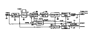
Referring now to Figs. 2 and 4, the video signal representing a magnified
image of
the area 18 is provided to a conventional sync stripper 50 that eliminates the
horizontal and
vertical pulses from the video signal. The output of the sync stripper 50 is
fed to the input
of a bandpass filter 52 having a transfer function H(c~). The filter has a
frequency response
that passes the high frequency components of the video signal for the reasons
given above.
The filter 52 produces a filtered signal representing the predetermined high
frequencies in
the image signal. The filtered signal is provided on an output of the filter
~~ that i~
connected to the input of a transient removal element 56. The transient
removal element
56 is gated by synchronization signals extracted from the video signal. In the
preferred
embodiment, the gating eliminates scanning artifacts produced at the beginning
and enduy
of each of the scan lines of the image signal. In effect, the transient
removal element 56
may also be regarded as a window generator which, for each scan line in the
video signal,
enables a window that is shorter than the scan line, with the respective ends
of the scan line
extending beyond the ends of the window. Provision of the vertical sync pulse
enables the
transient removal element 56 to produce a two-dimensional window that may
moved over
each of the two interlaced fields forming a frame of video in the typical
scanned format.
Tile transient removal element 56 provides the filtered signal, with scannin~~
artii~acts
removed therefrom, on an output that is connected to the input of squaring
circuit >8. ~f h~
squaring circuit squares the magnitude of the predetermined frequency
components in the
filtered signal, providing the squared magnitudes on an output that is
connected to the input
of an integrator 60. The integrator 60 integrates the squared magnitudes of
the fiequencv
components of the filtered signal, producing a focus index signal in analog
form that is
provided to a sample and hold circuit 62. The sample and hold circuit 62 is
gated to hold
a voltage magnitude of the integrated signal produced by the integrater 60.
The voltage
magnitude of the integrated signal (the focus index signal) represents a
degree of focus of
the microscope 12. The focus index signal is provided on the signal path 40 to
the
computer 34. The elements 52, 56, 58, 60, and 62 therefore form a focus index
part of the
analog portion of the analog circuit 36. An average illumination part of the
analog circuit
36 is formed by an integrator 68 that integrates the video signal. stripped of
ltS 1\'llc sl<~Ilals
CA 02283088 1999-08-04
WO 98/35256 PCT/US98I00318
-9-
by the sync stripper 50. The integration of the video signal by the integrator
68 over, for
example, a line of video, represents average illumination over the line. The
magnitude of
the integrator 68 is sampled and held by sample and hold circuit 70 whose
output forms the
average illumination signal provided on signal path 42.
The digital portion of the analog circuit 36 consists of a control timing
circuit 6(,
that receives the image signal intact, including all of its scanning
artifacts. such as vertical
and horizontal sync portions. The control timing circuit 66 generates reset
and hold signals
that sequentially synchronize the operations ofthe integrators 60 and 68 in
the sample and
hold circuits 62 and 70, respectively. In addition, the control timing circuit
66 produces the
trigger signal on the signal line 46.
The control timing circuit 66 further produces the sync signals necessary to
form
the window implemented by the transient removal element 56.
Digital Section
With reference to Figs. 2 and 4, the synchronization pulses of the video
signal are
detected in the control timing circuit 66 by a sync separator 80 (LM 1881.
National
Semiconductor, Arlington, TX) which extracts the horizontal and vertical
pulses. This
timing information is used to create a window that represents an area of the
image where
the focus function will be implemented. At the very least, the window allows
removal of
the discontinuities generated by the filter 52 at the ends of horizontal
lines. This portion
of the analog circuit 36 can be used as a mask generator to select an
arbitrary rectangular
portion of a video field for processing; any window size can be defined
vertically and
horizontally by changing the time constants of the two monostable
multivibrators. A first
portion of the window is established by flip flops 82a and 82b; the second
portion by flip-
flops 83a and 83b. This type of analog masking has been used for video-
dimension
analyzers. Yin, F.C.P., Tompkins, W.R., Peterson, K.L and Intaglietta M, "A
Video-
Dimension Analyzer," IEEE Transactions on Biomedical Engineering, 19(5),
pp.376-81.
1972. The window information is used by a gated amplifier 84 in the transient
removal
element 56. After each window, or video field, a trigger pulse is generated.
The control
timing circuit 66 also produces a sequence of 60 Hz trigger signals that gate
the computer
34 for A/D conversion of the corresponding analog values for each field.
CA 02283088 2002-04-15
_ _~7
t _ WO 98/35256 ~~ PCT/US9L~1003~8
Analog Section
The filter 52 is implemented with wide-bandwith monolithic amplifiers 90-c)6
having high slew rates and internal unity-gain frequency compensation for high
speed and
stability. Such high frequency, high-speed amplifiers are more prone to
oscillations than
low frequency devices. However, this instability was eliminated by reducing
the stray
capacitance at amplifier inputs and outputs. Power supply bypassing was also
used for
stability enhancement, and small capacitors were added parallel to the
feedback resistors
to compensate for unavoidable stray capacitance in the filters.
Figure 3a shows the plot of a horizontal video line 100 and selected-
subsequent
analog processed outputs. The sync stripper 50 removes the sync portion ofthe
composite
video signal per waveform 102. The reference level is at ground and since the
sync tip is
negative the output will have the sync removed and place the blanking level at
e~round.
After the video signal input is stripped of its synchronizing pulses, the
signal is fed to both
the filter 52 in the focus index section and the illumination integrator 68.
1 S Each of the operational amplifiers 90-96 of the f lter (LT1220, Linear
Technology
Corporation, Milpitas, CA) is used in a two-pole active Butterworth filter
configuration,
with the four operational amplifiers an-anged in a 4th order lowpass section
52a and a 4th
order highpass section 52b. A frequency response from 2 to 4 MHz was selected,
for
matching the digital filter response, which represents the transfer function
of the optics in
the microscope 12. A bandpass gain of 2.56 was used to compensate for signal
attenuation.
Due to the wide bandwidth and unity compensation of the components, good
performance
was obtained without further custom design. With the correct choice of the
components.
cutoff frequency is independent of amplifier bandwith, and is determined only
by the
respective R-C networks in the low-pass section 52a and the high-pass section
52b.
Manifestly, these networks may include manually-adjustable elements. Wavefc~rm
1 r4
demonstrates the filter output.
Filter 52 may, fox example, comprise an analog filter
with a transfer characteristic (H(c,~)) that passes only the
upper half of frequencies in the optical transfer charac-
teristic of the microscope.
a
CA 02283088 2002-04-15
- 10a -
The windowed, filtered signal is offset, amplified and squared. as shown in
waveforms 106 and 108. The filtered, squared signal is then integrated over
one video field
by the integrator 60. The integrator 60 includes reset, integrate and hold
control functions
to reset the capacitor 110 at the end of each field, integrate the riltered
signal for focus
index calculation, and, over the diode 114, hold intermediate focus while
there is no
CA 02283088 1999-08-04
WO 98135256 PCTIUS98100318
significant output from the filter 52. Previous analog autofocus circuit
designs, lacking the
hold control, exhibited focus index output decay between image features. This
is illustrated
clearly by waveform 109 in Fig. 3a, where, over the portion of the squared
waveform 108
marked "dead space", the magnitude of the integrated signal produced by the
integrator 60
does not decay. Using the integrator 60 with diode 114 instead of the
conventional
integrator ensures that the focus index more ideally matches the true
mathematical integral
for each video field. The output of the integrator 68 is similarly controlled
by capacitor 116
and diode 118.
The average illumination section takes the sync stripped video signal and
measures
the average illumination by integrating the signal over one field. A sample
and hold circuit
is used to maintain the final analog values for the A/D board. The final
output ti~om this
integration, and the focus index, are then converted by the analog-digital
board in the
computer 34. The trigger signal is sent to the computer at the end of each
field to start a
new conversion. Focus index, average illumination and trigger, with their
respective
grounds, are conventionally connected to the computer 34 or signal paths 40,
42 and 46,
respectively.
Windowing in the analog circuit 36 is shown in Fig. 3b, and can be understood
with
reference to Figs. 2 and 4. For the scan line dimension, a horizontal window
pulse 120 is
created for any line of video by the flip-flops 82a-82b in response to
horizontal line
blanking. A vertical window pulse 124 is produced by the flip-flops 83a-83b in
response
to vertical blanking. The transistor-diode circuit 126 responds to the pulses
120 and 124
as an AND gate, transmitting the filtered signal from the filter 52 to the
squaring circuit 58
when both pulses are high. Manifestly, counting or timing may be employed with
the tlip-
flops in the control timing circuit 66 to selectively adjust the dimensions of
a window.
Focusin~~ Software. Autofocus Al. or~'y ithm
In the focus processor 39, an interrupt service routine (ISR) was implemented
to
acquire the analog value of the focus index and average illumination signals,
based on the
trigger signal supplied by the analog circuit 36. This routine also controlled
focus position.
acquisition of the analog values from the autofocus circuit and calculation of
the
normalized degree of focus. Programs were written in C and assembler
languages. The C
CA 02283088 1999-08-04
WO 98135256 PCT/US98I00318
-12-
routines were compiled with Metaware High C (Santa Cruz, CA). A Phar Lap
(Cambridge,
MA) assembler was used for the interrupt service routines.
At the end of each field a trigger pulse starts the ISR, which transfers the
analog
values of the focus index and average illumination signals to arrays
accessible to C routines
for calculating and setting best focus.
In order to determine a best focus. the computer 34 executes a focus sequence
in
which the Z-axis position of the objective lens 14 is sequenced through a
plurality of focus
positions (z;). At each focus position the magnitude of the focus index and
average
illumination signals are taken and a focus function value (F(z;)) is
calculated according to
equation (2). Focus function values are stored at 130, Fig. l, by the computer
34.
After each focus sequence, with focus indices stored by the computer 34 for a
number of positions, a power-weighted average is used to find best focus.
Unusually
shaped focus curves containing multiple extrema may be produced by discrete
vertical
distributions of cellular components. For these reasons, the weighted average
~ z(F )n
yy = Z (' )
)
is used, where Wa is the power-weighted average position. z is the vertical (Z-
axis)
position, FZ is the result of the focus function (equation (?)) calculated
t~rom all Illlel~~t
acquired at one z position, and n is the power of the weighting. The power
accentuates the
peak values and the average reduces the effect of the 3D nature of the
specimen.
Experimental Results
Contrast in a microscope image is not an inherent property of a specimen.
Rather
it is a product of (1 ) the interaction of the illuminating light waves and
specimen structure
and (2) the MTF and contrast generation mode of the microscope. Point ( 1 }
depends both
in specimen structure and on the condition of the illuminating light wave;
point (2) depends
both on the condition of the illumination and how the waves leaving the
specimen are
treated. moue, S., "Video Microscopy", Plenum Press, New York, 1986.
Phase contrast microscopy was used as the imaging technique for autofocus in
these
experiments. In phase contrast, phase changes introduced by the transparent
cells are
CA 02283088 1999-08-04
WO 98I35Z56 PCT/US98I00318
-13-
transformed into changes in intensity. Born, M. and Wolf, E., "Principles of
Optics".
Pergamon Press, 1989. This creates contrast in the image that is useful for
performing
autofocus. Phase contrast also performs an optical highpass filter. moue. S..
"Video
Microscopy", Plenum Press, New York, 1986. Experimentally, phase contrast has
also
been shown to be more prone to exhibit side peaks in the focus function curve.
Price, .1.H.
et al., op. cit. Thus, it is important to carefully select the high
frequencies to ensure
unimodality.
In Figure 5 the plot of a phase-contrast experiment of a cell monolayer at
different
Z-axis positions is shown. Similar focus function curves are obtained by the
analog and
the digital versions, peak widths and sharpness of the functions are primarily
unimodal.
The curves exhibit damped side peaks outside the main lobe. This behavior is
exacerbated
by undersampling at unit zoom. Increasing the magnification results in the
Nyquist
sampling and this behavior is eliminated. The low cutoff of the filter
captures mid-range
frequencies for which a monotonic behavior cannot be assumed. The tendency
toward side
peaks is reduced with the increased frequency response of the focus index
system transfer
function, which includes the filter, CCD camera, and optical transfer
function.
Figure 6 shows a plot of the analog focus index using a thick cell monolayer.
The
3-D structure of the specimens creates differences of best focus and accounts
for the
broadening of the focus function. The increased specimen depth also seems to
enhance the
side peaks. Thus, the shape of the focus curve depends both on the specimen
and the
system transfer function. The sampling period for a particular experimental
condition was
calibrated using images of a micrometer slide with a 10 pm spacing. At a zoom
of 1 x
{using the 40x objective) the period was 303 nm. The resolving power is given
by the
Rayleigh criterion, d =1.227J(NAob~ + NA~o~a). With a S00 nm illumination. a
0.52 NA~a~a
and 0.85 NAob~, a resolution of 445 nm is obtained. The required Nyquist
sampling is then
222.5 nm. A magnification of (303/222.5) = 1.36x is thus required for Nyquist
sampling.
For a variety of practical reasons, one must, in fact, oversample further.
moue, S., op. cit.
The principal advantage of this carefully designed analog circuit is lo~~ cost
with
no performance sacrifice. The digital processing for real time autofocus
demands the use
of a real time image processor with pipeline architecture which can be an
order of
magnitude more expensive. In addition, increasing the complexity of the
digital filter
CA 02283088 1999-08-04
WO 98135256 PCT/US98/00318
-14-
involves adding coefficients, which can further increase cost or reduce speed.
On the other
hand, digital autofocus makes reprogramming a simple task, and for real time
operation.
the digital image processing resources can be used for simple one-dimensional
filters as
discrete approximations of the derivative filters (e.g. the { 1, -1 } and {-1,
2, -1 } highpass
filters and the { 1, 0, -1 } bandpass filter). Given the cost of the digital
image processing.
however, replacement of the digital implementation with an inexpensive analog
circuit of
equal performance that frees this important resource for other tasks may be
the most
important consideration.
One drawback with analog circuits in general (at least with respect to their
digital
equivalents) is limited dynamic range. The digital dynamic range is
proportional to the
square root of the product of the pixels and gray levels. Analog processing is
limited to the
number of bits of an A/D converter. Of course, the limited analog dynamic
range could be
overcome by addition of an automatic gain control circuit. On the other hand,
analogs
implementation permits an arbitrary upper cutoff frequency (up to the I imit
of the camera ).
whereas in the digital version this upper limit is set by the image processor.
Thls sllllpllfle5
matching the focus cutoff frequency in the filter 52 to the microscope optical
transfer
function to generate a sharper filter function curve for improved autofocus
reproducibility.
Assuming, a CCD camera capable of 768 pixels/line, image processor 3 8
digitized only 5 I 2
pixels/line. With the analog circuit 36, plug-in headers may be used for the
filter 52 to
simplify matching of the filter function with each video camera and optical
transfer
function combination. The analog circuit filter 52 is much easier and less
expensive to
change than the resolution of the image processor 38.
While the above detailed description has shown, described and pointed out the
fundamental novel features of the invention as applied to various embodiments.
it will be
understood that various omissions and substitutions and changes in the form
and details of
the device illustrated may be made by those skilled in the art, without
departing li-om the
spirit and scope of the claimed invention.