Note: Descriptions are shown in the official language in which they were submitted.
CA 02283396 1999-08-31
WO 98/39797 PCT/SE98/00388
1
SEMICONDUCTOR AND METHOD RELATING TO SEMICONDUCTORS
Technical Field
a The present invention relates to a manufacturing method for semiconductors.
$ackground
In silicon components, aluminium is often used as contacts to, for example.
the base
and the emitter. This has the following disadvantages:
Aluminium spiking may occur through thin pn junctions. resulting in short
circuits.
If pure aluminium is used, silicon from the surface can diffuse into the
aluminium.
leaving voids or non-homogenous regions below the aluminium contact.
If an alloy of aluminium with silicon is used the silicon can be deposited in
the
1 ~ contact areas in form of precipitates causing high contact resistance.
To avoid the above mentioned disadvantages which occur when aluminium comes in
direct contact with silicon, a barrier layer. for example of TiVV, is normally
used
between the silicon layer and the aluminium. In this case both n type and p
type
silicon must be doped under the contact surfaces to achieve low contact
resistance.
To avoid avalanche breakdown between n+ and p+ areas at low voltages, they
need
to be separated. The distance by which they are separated is important for the
characteristics of the component. The separation can be accomplished in
several
ways. One common way is to implant the dopants through two individual masking
layers. The second mask must be aligned to the first mask. Uncertainties in
this
alignment will always cause some lateral error between the layers.
If the component is to be doped both with acceptors and donors, as is the case
with
practically all semiconductors. the process of masking must be carried out
twice:
once masking out the parts which should not be exposed to acceptors before
dopin~~
with the p dopant, and once masking out the parts which should not be exposed
to
CA 02283396 1999-08-31
WO 98/39797 PCT/SE98/00388
7
donors before doping with the n dopant. Also, the masks must be dimensioned
and
applied very carefully to achieve doping of exactly the desired areas. There
is also a
risk that the dopant will not be completely restricted to the unprotected
areas.
US Patent Specification 4,4~ 1,844 discloses a semiconductor device
manufactured
using a layer of polycrystalline silicone (polysilicon) to cover the active
area of the
component. The masks used for covering parts of the component while doping are
applied on top of the polysilicon, and the component is doped through the
layer of
polysilicon.
US Patent Specification 5,451,532 describes a process for making a bipolar
transistor in which a polysilicon layer is used both as an emitter, which
raises above
the surface of the transistor, and, together with sidewall spacings, as a mask
when
doping the base contact, which is placed around the emitter.
l~
Summary of the Invention
Thus, it is an object of the invention to obtain a method for separation of
the n+ and
p+ areas in a semiconductor with high accuracy.
It is another object of the invention to achieve a high accuracy in the
distance
between of the n+ and p+ areas with very small distances.
It is yet another object of the invention to obtain a high area accuracy of
the area
2~ surrounded by the polysilicon area.
It is yet another object of the present invention to obtain a method for
doping both
n+ and p+ areas of semiconductor components without the need for two separate
masks.
JO
r i _ _ .M _.w. .
CA 02283396 1999-08-31
WO 98/39797 4 PCT/SE98/00388
Figure 1 is a cross-section of a part of a silicon component ready to be
processed
according to the invention;
Figures 2 A to 2F show different stages in the process of manufacturing a
component
according to a first embodiment of the invention, the component shown in cross
section:
Figure 2G shoves the component in cross-section, after it has been processed
according to the first embodiment of the invention, ready for further
processing
according to known methods;
Figures 3A to 3E show different stages in the process of manufacturing a
component
according to a second embodiment of the invention;
Figure 3F shows the component in cross-section, after it has been processed
according to the second embodiment of the invention, ready for further
processing
according to known methods;
Fiwre 4 is a schematic cross-sectional view of a resulting component according
to
an embodiment of the invention;
Figure ~ is a schematic cross-sectional view of a resulting component
according to
another embodiment of the invention;
Figure 6 is a schematic cross-sectional view of a resulting component
according to
yet another embodiment of the invention.
Detailed Description of Embodiments
Figure 1 shows a part of the silicon component ready to be processed according
to
the invention. The base area and part of the collector area are shown. On a
first layer
1 of carrier substrate, which may be, for example, a silicon layer with some
kind of
doping or an insulator, there is a layer 3 of n type silicon. forming part of
the
collector area. The n type silicon is just an example, and it will be readily
understood that the method can be applied to p type silicon as well, in which
case
the areas which are here p+ doped will be n+ doped and vice versa..
CA 02283396 1999-08-31
WO 98139797 PCT/SE98100388
J
The above mentioned objects are achieved according to the present invention by
depositing at least one selectively shaped area (I l'; 11") of a material or
combination of materials, that can be defined with high accuracy, so thick
that it will
not be penetrated by dopant ions, on the component to delimit the doped area
or
areas before the doping of the component is carned out using conventional
masking
techniques.
The material used may be polycrystalline silicon (polysilicon), silicon
nitride Si~N~,
or a silicide, such as TiSi~. CoSi,; or WSi,;. It may also be a combination of
any of
these and/or an oxide.
The invention has the following advantages:
It is possible to separate the n+ and p+ areas by a very small distance with
an
accuracy better than 0,1 ~m without additional masking steps in the
manufacturing
process.
The SiO~ area covering the component underneath the polysilicon area provides
a
surface of high quality, with a minimum number of crystal defects and surface
states
causing leakage currents.
If the preceding processing of the component involves depositing a polysilicon
layer,
one masking step less is required in the method according to the invention
compared
to prior art methods. This is particularly useful in BiCMOS processes, that
is, when
MOS components and bipolar components are used together.
Brief Description of the Drawings
The invention will be described in more detail in the following, with
particular
reference to the drawings. on which:
r r
CA 02283396 1999-08-31
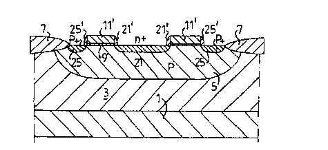
WO 98/39797 5 PCT/SE98/00388
An area 5, which is the base area and has the opposite doping from the
collector area
3, is delimited by an oxidized area 7 covering the surface of the component in
an
area around the base area.
J
To this component, first a layer of Si02 is applied either by oxidizing the
surface by
means of heat treatment in an oxidizing atmosphere, or covering the component
with
a layer of Si02. Then a layer of polysilicon is applied on top of the Si02
layer. In the
described embodiments, polysilicon is used. As mentioned above, other
material,
such as silicon nitride, a silicide or a combination of nitride, polysilicon,
silicide
and/or oxide could be used instead.
Figure 2A shows the upper part of the silicon component after these two steps
have
been carried out. A layer 9 of Si02 covers the component over the entire
active area
1 ~ 5, and a layer 11 of polysilicon covers the Si02 layer 9.
The polysilicon layer 11 is then doped to decrease the resistivity of the
layer. Then it
is oxidized to create a protection layer for fiu~ther process steps, and the
dopant used
is activated.
Next, the polysilicon layer 11 and the Si02 layer 9 are to be etched back,
except
where it will be used in the process to follow. This is done by masking out
the areas
to be kept, using masking techniques well known to the person skilled in the
art.
First the component is oxidized again so that an Si02 layer forms on top of
the
2~ component, then the mask is applied.
Figure 2B shows the component at this stage. On the active area of the
component,
one or more areas are covered by a first layer 9 of Si02, a layer 11 of
polysilicon, a
second layer 1 ~ of Si02 and a layer 1 ~ of the substance used to mask out the
area.
Two parts 15' have been treated so that they will not be etched back in the
first
CA 02283396 1999-08-31
WO 98/39797 PCT/SE98/00388
6
process. thus masking out the areas of the component on which the polysilicon
layer
11 will remain.
Figure 2C shows the situation after the covering layers 9, 1 I. 13, 15 have
been
etched back. In the selected areas, the component is covered with one layer 9'
of
Si02, a polysilicon layer 11' on top of that, then another layer 13' of Si02
and then
the mask layer 15'.
Next, the mask layer 15' and the Si02 layer I3' are removed using techniques
well
known to the person skilled in the art. As shown in figure 2D, the resulting
component is covered in the selected areas with one Iayer 9' of Si02 and one
layer
11 ' of polysilicon.
The surface is oxidized. resulting in a thin oxidized layer 17 shown in figure
2E. The
layer 17 must be so thin that the dopant will reach through it to dope the
component.
The thickness of the oxide layer 17 depends on the kind of dopant used and the
energy with which the dopant ions are implanted. Typical values are 150-500
.~.
A mask 19 defining an emitter area 21 has been applied and the component is
ready
for doping with an n+ dopant to form the emitter 21. As can be seen in figure
2E,
this mask does not have to be fitted exactly to the emitter area 21, but only
has to be
fitted to some part of the upper surface of the polysilicon layer 11'. The
mask 19 and
the polysilicon layer 11' ensure that only the emitter area 21 is doped.
The next step is to remove the mask 19. Then a new mask 23 is applied to cover
the
emitter 21 as shown in figure 2F . It may be seen that this mask also does not
have to
be fitted exactly. The component is then exposed to a p+ dopant. The result is
the
doping of p+ in the areas not covered by the mask 23, the polysilicon layer
11' or by
the oxide layer 7, which delimits the active area of the component.
The mask 23 and the oxide layer 17 are then removed. If desirable, of course
the
polysilicon Iayer may also be removed.
T ....._ r
CA 02283396 1999-08-31
WO 98/39797 PCT1SE98/00388
Figure 2G shoves a cross-section of the resulting component. A p area 5 in the
silicon
component is delimited by the oxide layer 7. The component as shown has one n+
doped emitter area 21 and one, ring shaped p+ doped base area 25. The n+ doped
S area 21 and the p+ doped area 25 are separated by the polysiiicon area 11',
which in
this case is rinb shaped. Remaining parts 21', 25' of Si02 may be found on the
sides
of the polysilicon Iine 11'. These parts 21' and 2~' will be n+ doped and p+
doped
respectively. However, this will not affect the performance of the component.
It is possible to simplify the above process by reducing the number of mask
layers
required in the process, in the following way: The first steps of the process
are the
same as described for figures 2A to 2D.
Figure 3A shows the same situation as in figure 2D. On a first layer 1', of a
carrier
1~ substrate which may be, for example, a silicon layer with some kind of
doping or an
insulator, there is a layer 3' of n type silicon, forming part of the
collector area. The
n type silicon is just an example, and it will be readily understood that the
method
can be applied to p type silicon as well. An area 5', which is the base area
and the
opposite doping of the collector area 3', is delimited by an oxidized area 7'
covering
the surface of the component.
One or more areas of Si02 9" and polysilicon 11" cover part of the base area
~'.
Next, an thin protective Si02 layer 31 is deposited or oxidized on the
component, as
shown in figure 3B. Then the device is covered by a second protective layer
33, for
example Si~N4, which can protect the underlying silicon from oxidation. Using
a
masking layer 35, the second protective layer 33 is removed from the parts of
the
device which should be oxidized in future steps.
Then the mask layer is removed to produce the component as shown in figure 3C.
The component is entirely covered by a thin oxide Iayer 31, and paz-ts of the
component are covered by the remaining part of the second protective layer
33'. The
CA 02283396 1999-08-31
WO 98/39797 PCT/SE98/00388
g
next step is to implant the selected dopant, in this case an p+ dopant, by ion
implantation. so that the areas that are not protected by the second
protective layer
3' will be doped. The ions will penetrate each layers to a certain extent, so
that the
component will be doped down to a certain level, shown as a dotted Iine 39. As
a
~ result, the areas of the silicon component not covered by the second
protective layer
JJ' or by the field oxide layers 7' will be doped with an p+ dopant.
Then the component is oxidized, and the p+ dopant is activated. The areas
covered
by the second protective layer 3J' will not be oxidized. As shown in figure
3D, the
oxide layer 31' is thicker than the layer 31 in figure 3C, except where the
component
is covered by the second protective Iayer 33'. The oxide layer 31' must now be
so
thick that the dopant will not be able to penetrate it completely, that is, it
must
protect the component from being doped in the areas covered by the oxide layer
31'.
The polysilicon areas I l" are partly oxidized and therefore obtain an
irregular shape.
Next, the second protective layer 33' is removed. As shown in figure 3E, the
Si02
layer 31' is now so thick that the a new dopant will not be able to penetrate
it, except
in those areas where the second protective layer 33' prevented further
oxidation. The
component is then doped with an n+ dopant, which will penetrate all layers to
a
certain extent, shown with a dotted line 43. Hence, only the area 45 which was
covered by the second protective layer 33' will be n+ doped.
In a final step, the oxide layer can be removed, to produce the component as
shown
in figure 3F. An p+ doped base area 41 and an n+ doped emitter area 45 are
separated by a line of polysilicon i 1''. On the edges of the polysilicon line
1 I" some
Si02 41', 45' remains. These areas are doped with the same dopant as the
adjacent
areas 41 and 45 respectively and, as in figure 2G, will not affect the
characteristics
of the component.
Subsequently, the component is processed according to known methods, to
produce
the final semiconductor component.
T
CA 02283396 1999-08-31
WO 98/39797 PCT/SE98/00388
9
Figure 4 is a schematic representation of cross-sectional view of a component
after
the final processing. The layout of the component is chosen only as an
example; it
could be any kind of bipolar component. This kind of component is normally
used
for vertical bipolar components, for example if no galvanic insulation from
the
surrounding components is needed. A carrier layer 101 consists of a
semiconductor,
such as silicon, doped with the same kind of dopant as an adjacent layer 103,
but to
a different, normally higher, degree. In the adjacent layer I 03, which
constitutes the
collector area of the component, there is an area 105 with the opposite type
of
doping which constitutes the base area.
The whole component is covered by an insulating layer 107, which may be a 0.5 -
3 ~.un thick layer of oxide. In the base area 105, there is an emitter 121 and
a base
125, separated by a polysilicon area 109 on the surface. There is a first
contact 131
to the base 125. a second contact 133 to the emitter I21 and a third contact
135 to
the collector 103. .411 contacts are only shown schematically. The contacts
can be
made using standard techniques for semiconductor device manufacturing,
including
steps such as deposition and etching of metals and insulating materials.
Figure 5 is a schematic representation of cross-sectional view of a component
after
the final processing. This type of component is used when the component must
be
electrically separated from surrounding components on the same chip. The
layout of
the component is chosen only as an example; it could be any kind of bipolar
component. A lower carrier layer lOlA, consists of a semiconductor, such as
silicon,
doped with the opposite kind of dopant than an adjacent layer 103' which
constitutes
the collector area of the component. An upper carrier layer lOlB may be
situated
between the lower carrier layer lOlA and the collector layer 103'. If present,
the
upper carrier layer lOlB is doped with the same type of dopant as the
collector layer
103 ", but to a different, normally higher, degree than the collector layer
103' .
3O
CA 02283396 1999-08-31
WO 98/39797 PCT/SE98/00388
The upper lOlB carrier layer, if present, serves to reduce the resistance in
the
collector area.
In the collector layer 103' there is an area 105' with the opposite type of
doping,
5 which constitutes the base area. and an area 127' which constitutes the
collector
contact area. In the base area 105', there is an emitter 12I' and a base 125',
separated by a polysilicon area 109' on the surface. There is a first contact
131' to
the base 125', a second contact 133' to the emitter 121' and a third contact
135' to
the collector I03'. All contacts 131', 133', 135' are only shown
schematically.
The whole component is covered by an oxidized layer 107' and separated from
the
adjacent components by vertical bars 129' of insulating material extending
through
the collector area layer 103' and, if applicable, the upper carrier layer
lOlB. The
vertical bars 129' may consist of p doped silicon, an insulator such as Si02
or a
combination of different insulator materials and semiconductor materials. such
as
polysilicon; Si02 and Si3N4.
Figure 6 is a schematic representation of cross-sectional view of a component
after
the final processing. The layout of the component is chosen only as an
example; it
could be any kind of bipolar component. This kind of component is particularly
suitable when there is an underlying substrate which is not part of the
component.
from which the component has to be galvanically insulated, for example to
reduce
the leakage current or to improve the high voltage performance of the
component. A
lower carrier layer 11 lA, consists of an insulating material. An upper
carrier layer
111B may be situated between the lower carrier layer 111A and the collector
layer
103". If present, the upper carrier layer 111B is doped with the same type of
dopant
as the collector layer 103", but to a different, normally higher, degree than
the
collector layer 103".
The insulating carrier layer 111A rests on a substrate 111C, and is used to
achieve a
galvanic insulation from fhe substrate 111 C, which may be, for example, a
~ .r
CA 02283396 1999-08-31
WO 98/39797 PCT/SE98/00388
11
semiconductor. an insulator, a metal or an organo-metallic compound. If both
the
upper 111B, and the lower 111A carrier layers are used. the upper carrier
layer 111B
will reduce the resistance in the collector area 103". If the resistance in
the collector
area is not critical, the upper carrier layer 111B may be omitted.
In the collector layer 103" there is an area lOS" with the opposite type of
doping
which constitutes the base area and an area 127" which constitutes the
collector
contact area. In the base area 10~", there is an emitter 121" and a base 125",
separated by a polysilicon area 109" on the surface. There is a first contact
131" to
the base 125". a second contact 133" to the emitter 121" and a third contact
135" to
the collector 103". All contacts 131". 133", i35" are only shown
schematically.
The whole component is covered by an oxidized layer 107" and separated from
the
adjacent components by vertical bars 129" of insulating material extending
through
1~ the collector area layer 103" and, if applicable, the upper carrier layer
111B. The
vertical bars 129' may consist of p doped silicon, an insulator such as Si02
or a
combination of different insulator materials and semiconductor materials, such
as
polysilicon. Si02 and Si3N4.
The semiconductor layers 101, lOlA, lOlB, 111B may consist of any kind of
semiconductor, such as silicon, silicon carbide (SiC) or any element from the
third
or fifth row of the periodic system (III-V material). The insulating layer 11
lA may
be, for example, Si02, A1203, diamond, Si3N4, quartz (crystalline Si02) or
glass. The
substrate 111 C may be any of these.
The embodiments described above have been discussed for a ring shaped area.
but it
is obvious that the polysilicon areas 11', 11'', 109. 109', 109" in the
figures could be
given any desired shape and that more than one polysilicon area could be used.
depending on the type of component to be manufactured. Similarly, the doped
areas
2~, 41 could be two areas provided on each side of the central area 21, 11.
CA 02283396 1999-08-31
WO 98/39797 PCT/SE98/00388
12
The order in which the emitter and the base areas are defined may also be
chosen
arbitrarily.
~ ~