Note: Descriptions are shown in the official language in which they were submitted.
CA 02284044 1999-09-17
WO 98/43248 PCT/EP97/02112
-1-
COMPUTER MEMORY ORGANIZATION
The present invention relates to computer memories, and more specifically to
the
division of memory areas therein and/or to the updating of the contents of
flash
memory. It finds particular application in ~a receiver/decoder of .a broadcast
and
reception system, in particular a receiver/decoder of a digital interactive
satellite
television and/or radio system. However, it will be realized that it is not
limited to
that system or systems of that type, but is applicable more generally to a
wide variety
of computer systems.
In computer systems, particularly systems where the computer system is
incorporated
in some larger system such as a receiver/decoder for digital television or
radio, the
amount of memory is often limited. This means that the memory must be
organized
so that the use of memory space by the various functions required by the
system is
minimized. In addition, it may also be necessary to minimize the time required
to
access at least some parts of the memory.
One aspect of the present invention is particularly concerned with the
provision or
organization of buffers in the memory.
The conventional technique for providing buffers is by a dynamic system for
allocating the required buffers. However, in the present context this standard
system
has certain disadvantages. It tends to result in fragmentation of the memory,
and its
speed is restricted by the need for overhead operations. Also, if an expansion
of the
buffers is required, it may require movement of blocks of memory to create
space for
the expansion.
According to one aspect of the present invention there is provided a system
for
defining and addressing buffers in a memory area in a computer system,
comprising:
pool size storage means for storing a plurality of pool sizes; buffer size
storage means
for storing, for each pool, a buffer size; and calculating means for
calculating
therefrom the address of a desired buffer in a desired pool. Preferably means
are
CA 02284044 1999-09-17
WO 98/43248 PCT/EP97/02112
-2-
included for determining the pool sizes in cumulative form and storing them in
that
form in the pool size storage means. A reserved area may be defined at the
beginning
of each pool, and_means provided for selecting either the cumulative pool size
direct
or the output of the calculating means. 'Fhe desired pool number, desired
buffer
number, and desired byte may be checked for out-of=bounds values.
A variety of types of computer memory are now available. One major distinction
between different kinds of memory is between volatile and non-volatile
memories.
Volatile memory retains its contents only while power is supplied to the
memory,
losing its contents as soon as its power supply goes off, while non-volatile
memory
retains its contents indefinitely even if its power supply goes off. The other
major
distinction is between writable memory and read-only memory.
Volatile memory is generally known as RAM, while there are various kinds of
non-volatile memory. RAM is non~nally writable, while read-only memory is
known
as ROM. This latter distinction is not necessarily hard-and-fast. Any memory
must
of course be writable in some sense at least once, but some kinds of ROM-like
memory can have their contents changed, albeit with some difficulty. Thus
there are
memory types such as PROM (programmable (ie writable) read-only memory,
EEPROM (electrically erasable programmable read-only memory), and Flash.
The different kinds of memory have different characteristics (eg different
read times
and different casts), so it is often desirable to use a combination of several
different
kinds in a single computer system.
Another aspect of the present invention is concerned with flash memory. A
flash
memory is generally ROM-like, in that it is non-volatile. It is also intended
to be
used in a generally ROM-like manner, being read from but not written to.
However,
flash memory can be written to, but only with some difficulty. Specifically, a
flash
memory is normally divided into pages, typically each of many kilobytes in
length,
and writing to the flash memory is by page. In more detail, to write to the
flash
memory, an entire page has to be erased and the new contents then have to be
written
CA 02284044 1999-09-17
WO 98/43248 PCT/EP97/02112
-3-
into the erased page; further, this writing has to be essentially a single
uninterruptible
operation. (Obviously there can be a gap between the erasing and the writing.)
In principle, the information in the flash memory may be organized into units
of any
size from a single word upwards. In practice, however, it will normally be
organized
into blocks of substantial size. A block may comprise data, eg tables of
permanent
or semi-permanent information, or a program or sub-routine. The block sizes
will
normally be chosen to be less than the page size (if a block is larger than a
page, it
will usually be feasible to split it into sub-blocks which are less than the
page size).
Typically, when a flash memory is updated it is desirable to retain some of
the
information already in it. This therefore requires the page being updated to
be read
into RAM to form an image of the page; this image in RAM can then be updated
by
inserting whatever new information is to be entered into the page. At the same
time,
any information in the page which is not longer required can be deleted. The
updated
image can then be written back into the flash memory.
In general, the block size will not be fixed; that is, different blocks will
be different
sizes. This can obviously cause difficulty when some existing blocks are to be
discarded and fresh blocks are to be added. These difficulties can largely be
overcome by allowing the blocks to the movable, so that when a page is
updated, the
blocks to be retained in the page are rearranged so that any unused areas on
the page
are merged into a single large unused area.
If the blocks are movable, then they cannot be addressed by fixed addresses.
Instead,
some sort of block locating or addressing data structure must be maintained so
that
the blocks can in effect be searched for by using some kind of name or
descriptor.
With blocks of different sizes, this requires information about both the
locations and
the nature of the blocks. This can be achieved in various ways. Thus a
detailed
directory of the blocks (their locations and nature) can be maintained at the
beginning
of the flash memory, or a location directory of the blocks can be maintained
at the
beginning of the flash memory and each block can include a header giving the
nature
CA 02284044 1999-09-17
WO 98/43248 PCT/EP97/02112
-4-
of the block. Alternatively, a separate block locating data structure can be
maintained
for each page of the flash memory.
All these block locating data structures have the common characteristic that
updating
of the flash memory is required for every change in its contents. To write a
fresh
block obviously requires flash memory updating; deletion of a block similarly
requires
updating. Although it is not necessary to physically delete the block, the
block
locating data structure has to be updated to indicate that the block is no
longer valid.
We have realized that the need for flash memory updating can be restricted to
the
addition of fresh blocks; in other words, blocks can effectively be deleted
without
requiring updating of the flash memory. To achieve this, the block locating
data
structure is held at least partially in an external memory outside the flash
memory
itself, preferably in an EEPROM memory.
The external memory may hold the substantially the entire block locating data
structure, ie the block addresses and descriptors. Alternatively, the external
memory
may hold only the locations of the blocks in the flash memory, with the
descriptors
of the blocks being included in the flash memory as headers of the blocks
themselves.
In both cases, the external directory may be organized either as a single
structure for
the entire flash memory or on a per page basis.
However, it is preferred to minimize the size of the external memory by
maintaining
in it only the validity of each block, with the block addresses and
descriptors being
maintained in the flash memory itself. This reduces the external memory to a
bitmap
of the validity of the blocks. To erase a block in the flash memory, all that
is
required is to change the bit for that block in the external memory from
"valid" to
"invalid" .
Returning to the general page updating procedure discussed above, this
procedure has
a problem. If the power supply to the system should be interrupted during this
procedure (or some other major system interrupt or crash should occur), the
contents
CA 02284044 1999-09-17
WO 98/43248 PCT/EP97/02112
_5_
of the RAM will be lost, so the updated image of the page being written into
the flash
memory will be lost. The information previously in the flash memory page being
updated will have been erased, as a preliminary to the writing of the updated
page
back into the flash memory. (And the updated page will have been written back
into
the flash memory only partially, so some of its contents will have been lost;
and, since
the precise point at which the power loss occurred will generally not be
known, it will
not normally be known exactly how much of the contents of the updated page
have
been written into the flash memory.)
One object of the present invention is to alleviate~or overcome this problem.
According to this aspect, the present invention provides a flash memory system
in a
computer wherein the flash memory is divided into separately writable pages,
comprising: means for copying a page of the flash memory as an image page into
RAM memory and updating the image page; means for writing the image page back
into a different page in the flash memory; a main record table, held in a
separate
non-volatile memory, identifying valid pages in the flash memory; and means
for
updating the main record table when a page in the flash memory has been
updated.
The memory holding the main record table is preferably EEPROM memory. Access
to the flash memory will normally be via the main record table.
In normal operation, the main record table will record some pages of the flash
memory as valid and others as invalid, "invalid" meaning that the page does
not
contain valid information. A page can be invalid in various ways; thus it may
be
empty, it may have been successfully copied into another page, or it may have
had its
writing interrupted.
In the present system, updating a page involves copying the page being updated
from
its existing page in the flash memory to another page (with the copying
involving
updating of the contents of the page). So the present system must always
maintain
at least one page as invalid; the invalid page or pages can equally well be
described
as "spare". When a page is updated, the main record table is updated only
after the
CA 02284044 1999-09-17
WO 98/43248 PC'T/EP97/02112
-6-
copying of the page is completed. Thus if the copying of a page is
interrupted, the
main record table will remain unchanged, so the original page wil! remain
valid and
the new page will remain marked as spare. The copying can either be re-tried
later
or abandoned.
Even with the system just described, there is a potential difficulty. The
system as so
far described relies on the updating of the main record table. It is therefore
important
to ensure that the integrity of this main record table is high.
Since the updating of the main record table will be very rapid compared to the
updating of a page of the flash memory, it may be possible to check the state
of the
power supply immediately before updating the main record table, using a power
supply which has sufficient capacity to maintain the system operating for at
least as
Iong as is required to update the main record table. Preferably, however, the
main
record table includes an error detection section and is itself copied into a
back-up
record table immediately after it has been updated. The system will then
include
means for checking the main record table for error when using it to access the
flash
memory, and for using the back-up record table if the main record table has an
error.
Thus if the main record table has an error; the system treats the last
updating of the
flash memory as invalid, just as if the updating had been interrupted.
It is of course possible for the copying of the main record table into the
back-up
record table to be interrupted. This copying occurs only after the main
updating of
the main record table has been completed, however. Any later access of the
flash
memory will involve the checking of the main record table; that main record
table will
be error-free, so the back-up record table will not need to be accessed and
its faulty
state will be irrelevant.
During the next updating of the flash memory, however, the main record table
will be
updated. This updating may be interrupted, as discussed above, and if it is,
then the
back-up record table has to be used to access the flash memory as it was
before the
updating. It is therefore undesirable to allow the back-up record table to be
faulty.
CA 02284044 1999-09-17
WO 98/43248 PCT/EP97/02112
This can conveniently be achieved by copying the main record table into the
back-up
record table as the first step in updating the flash memory (or at least
before the
writing of the updated image page from the RAM into the spare page of the
flash
memory).
It follows from the above discussion that the information or data blocks in
the flash
memory are not located in fixed positions. As the flash memory pages are
updated,
so the data blocks in them move from page to page, and may also have their
positions
in the page changed. Some form of directory is therefore required, so that the
data
blocks can be found when required. This directory information can be held in
the
record table or in the flash memory pages themselves, or divided between those
two
locations.
We have realized that in general the directory information does not normally
change
unless the data blocks themselves are changed, so it is therefore convenient
to store
it in the flash memory along with the data blocks. However, there is one
element of
directory-type information which may change without the data itself changing;
that
is, whether or not a data block is valid. It is therefore convenient to store
data block
validity information in the record table. This allows a data block to be
effectively
deleted without having to update the flash memory; all that need be done is to
change
the block's indicator from valid to invalid.
Of course, if the page with that block is updated at some later time, the
blocks with
invalid indicators will not be copied from the page into the image page in RAM
memory, so they will be deleted in a more physical sense at that point. ('They
will
actually remain in the old page, which becomes the new spare page, but are of
course
inaccessible there, and when that new spare page is used for the next updating
of the
flash memory, their physical deletion will be complete.)
The record table therefore preferably contains, for each page, a set of data
block
validity indicators, which may conveniently be in the form of single bits.
This
increases the size of the record table, which in turn means that a variety of
standard
CA 02284044 1999-09-17
WO 98/43248 PCT/EP97/02112
_g-
techniques can be used to provide the error detection section; it is preferred
to use a
cyclic redundancy check (CRC), though an error detecting or correcting code or
a
hash-type function could be used.
The block validity indicators for a page in the record table must of course be
linked
to the blocks themselves in that page in the flash memory. This may be done by
keeping the blocks in the page in the flash memory in the same sequence as
their
indicators in the record table. It is preferred, however, to provide a header
in each
page in the flash memory which contains a set of pointers to the actual
locations of
the blocks in that page; this permits greater freedom in the arrangement of
the blocks
themselves in the page.
The identification information (eg block name) for each block in the page may
be
included either in the page header or as a block header at the start of the
block itself.
The latter option is the one adopted in the preferred embodiment. This
identification
information may include block linking information, so that a large unit of
data can be
split into 2 or more blocks.
A further aspect of the present invention provides a recciver/decoder for use
in a
digital broadcast and reception system including a system or memory system or
flash
memory as described above.
Preferably, the receiver/decoder further comprises means for receiving a
compressed
MPEG-type signal, means for decoding the received signal to provide a
television
and/or radio signal and means for supplying the signal to a television and/or
radio.
Preferred features of the present invention will now be described, purely by
way of
example, with reference to the accompanying drawings, in which:-
Figure 1 shows the overall architecture of a digital television system
according to the
preferred embodiment of the present invention;
CA 02284044 1999-09-17
WO 98/43248 PCT/EP97/02112
_g_
Figure 2 shows the architecture of an interactive system of the digital
television
system;
Figure 3 shows the arrangement of files within a module downloaded into the
memory
of an interactive receiver/decoder;
Figure 4 is a simplified block diagram of the relevant parts of the computer
system;
Figure 5 is a diagram of the organization of a part of the RAM memory;
Figure 6 shows the structure of a Set Buffers command;
Figure 7 is diagram of the structure of the memory management unit.
Figure 8 is a block diagram of the system;
Figure 9 shows the logical layout of the flash memory and the record tables;
and
Figure 10 shows the logical layout of a flash memory page and a sub-section of
the
record table.
An overview of a digital television system 1000 is shown in Figure 1. The
invention
includes a mostly conventional digital television system 2000 which uses the
known
MPEG-2 compression system to transmit compressed digital signals. In more
detail,
MPEG-2 compressor 2002 in a broadcast centre receives a digital signal stream
(typically a stream of video signals). The compressor 2002 is connected to a
multiplexes and scrambler 2004 by linkage 2006. The multiplexes 2004 receives
a
plurality of further input signals, assembles one or more transport streams
and
transmits compressed digital signals to a transmitter 2008 of the broadcast
centre via
linkage 2010, which can of course take a wide variety of forms including
telecom
links. The transmitter 2008 transmits electromagnetic signals via uplink 2012
towards
a satellite transponder 2014, where they are electronically processed and
broadcast via
CA 02284044 1999-09-17
WO 98/43248 PCT/EP97/02112
-10-
notional downlink 2016 to earth receiver 2018, conventionally in the form of a
dish
owned or rented by the end user. The signals received by receiver 2018 are
transmitted to an.integrated receiver/decoder 2020 owned or rented by the end
user
and connected to the end user's television set 2022. The receiver/decoder 2020
decodes the compressed MPEG-2 signal into a television signal for the
television set
2022.
A conditional access system 3000 is connected to the multiplexes 2004 and the
recciver/decoder 2020, and is located partly in the broadcast centre and
partly in the
decoder. It enables the end user to access digital~television broadcasts from
one or
more broadcast suppliers. A smartcard, capable of deciphering messages
relating to
commercial offers (that is, one or several television programmes sold by the
broadcast
supplier), can be inserted into the receiver/decoder 2020. Using the decoder
2020 and
smartcard, the end user may purchase commercial offers in either a
subscription mode
or a pay-per-view mode.
An interactive system 4000, also connected to the multiplexes 2004 and the
receiver/decoder 2020 and again located partly in the broadcast centre and
partly in
the decoder; enables the end uscr to interact with various applications via a
modemmed back channel 4002.
Figure 2 shows the general architecture of the interactive television system
4000 of
the digital television system 1000 of the present invention.
For example, the interactive system 4000 allows an end user to buy items from
on-
screen catalogues, consult local news and weather maps on demand and play
games
through his television set.
The interactive system 4000 comprises in overview four main elements:
an authoring tool 4004 at the broadcast centre (or elsewhere) for enabling a
broadcast supplier to create, develop, debug and test applications;
an application and data server 4006 the broadcast centre, connected to the
CA 02284044 1999-09-17
WO 98/43248 PCT/EP97/02112
-11-
authoring tool 4004 for enabling a broadcast supplier to prepare, authenticate
and
format applications and data for delivery to the multiplexer and scrambler
2004 for
insertion into the _MPEG-2 transport stream (typically the private section
thereof) to
be broadcast to the end user;
a virtual machine including a run time engihe (RTE) 4008, which is an
executable code installed in the receiver/decoder 2020 owned or rented by the
end user
for enabling an end user to receive, authenticate, decompress, and load
applications
into the working memory 2024 of the receiver/decoder 2020 for execution. The
engine 4008 also runs resident, general-purpose applications. The engine 4008
is
independent of the hardware and operating system; and
a modemmed back channel 4002 between the receiver/decoder 2020 and the
application and data server 4006 to enable signals instructing the server 4006
to insert
data and applications into the MPEG-2 transport stream at the request of the
end user.
T3e interactive television system operates using "applications" which control
the
functions of the receiver/decoder and various devices contained therein.
Applications
are represented in the engine 4008 as "resource files". A "module" is a set of
resource
files and data. Several modules may be required to make up an application. A
"memory volume" of the receiver/decoder is a storage space for modules. An
"interface" is used to download modules. Modules may be downloaded into the
receiver/decoder 2020 from the MPEG-2 transport stream.
The elements mentioned in the previous paragraph are now described in more
detail.
For the purposes of this specification, an application is a piece of computer
code for
controlling high level functions of preferably the receiver/decoder 2020. For
example,
when the end user positions the focus of a remote controller on a button
object seen
on the screen of the television set 2022 and presses a validation key, the
instruction
sequence associated with the button is run.
An interactive application proposes menus and executes commands at the request
of
the end user and provides data related to the purpose of the application.
Applications
CA 02284044 1999-09-17
WO 98/43248 PCT/EP97/02112
-12-
may be either resident applications, that is, stored in the ROM (or FLASH or
other
non-volatile memory) of the receiver/decoder 2020, or broadcast and downloaded
into
the RAM or FLASH memory of the receiver/decoder 2020.
Examples of applications are:-
~ An Initiating Application. The receiver/decoder 2020 is equipped with a
resident initiating application which is an adaptable collection of modules
(this
term being defined in more detail hereunder) enabling the receiver/decoder
2020 to be immediately operative in the MPEG-2 environment. The
application provides core features which can be modified by the broadcast
supplier if required. It also provides an interface between the resident
application and downloaded applications.
A Startup Application. The startup application allows any application, either
downloaded or resident, to run on the receiver/decoder 2020. This application
acts as a bootstrap executed on arrival of a service in order to start the
application. Startup is downloaded into RAM and therefore can be updated
easily. It can be configured so that the interactive applications available on
each channel can be selected and run, either immediately after downloading or
after preloading. In the case of preloading, the application is loaded into
the
memory 2024 and is activated by the startup when required.
~ A Program Guide. The Program Guide is an interactive application which
,gives full information about programming. For example, it may glut
information about, say, one week's television programmes provided on each
channel of a digital television bouquet. By depressing a key on the remote
controller 2026, the end user accesses an add-on screen, overlaid on the evcnt
shown on the screen of the television set 2022. This add-on screen is a
browser giving information on the current and next events of each channel of
the digital TV bouquet. By depressing another key on the remote controller
2026, the end user accesses an application which displays a list of
information
on events over one week. The end user can also search and sort events with
simple and customised criteria. The end user can also access directly a
selected
channel.
CA 02284044 1999-09-17
WO 98/43248 PCT/EP97/02112
-13-
A Pay Per View application. The Pay Per View Application is an interactive
service available on each PPV channel of the digital TV bouquet in
conjunction with the conditional access system 3000. The end user can access
the application using a TV guide or channel browser. Additionally, the
application starts automatically as soon as a PPV event is detected on the PPV
channel. The end user is then able to buy the current event either through his
daughter smartcard 3020 or via the communication server 3022 (using a
modem, a telephone and DTMF codes, M1IVITEL or the like). The application
may be either resident in the ROM of the receiver/decoder 2020 or
downloadable into the RAM of the decoder 2020.
A PC Download application. On request, an end user can download computer
software using the PC download application.
A Magazine Browser application. The magazine browser application comprises
a cyclic video broadcast of images with end user navigation via on-screen
buttons.
A Quiz application. The quiz application is preferably synchronised with a
broadcast quiz programme. As an example, multiple choicc questions are
displayed on the screen of the television 2022, and the user can select an
answcr using the remote controller 2026. The quiz application can inform the
user whether the answer is correct or not, and can keep count of the user's
score.
A Teleshopping application. In one example of the teleshopping application,
offers of goods for sale are transmitted to the receiver/decoder 2020 and
displayed on the television 2022. Using the remote controller, the user can
select a particular item to buy. The order for the item is sent via the
modemmed back channel 4002 to the application and data server 4006 or to
a separate sales system the telephone number of which has been downloaded
to the receiver/decoder, possibly with an order to debit the account for a
credit
card which has been inserted into one of the card readers 4036 of the
receiver/decoder 2020.
A Telebanking application. In one example of the telebanking application, the
user inserts a bank card into one of the card readers 4036 of the
CA 02284044 1999-09-17
WO 98/43248 PCT/EP97/02112
-14-
receiver/decoder 2020. The receiver/decoder 2020 dials up the user's bank,
using a telephone number stored in the bank card or stored in the
receiver/decoder, and then the application provides a number of facilities
which
can be selected using the remote controller 2026, for example for downloading
via the telephone line a statement of account, transferring funds between
accounts, requesting a cheque book, etc.
An Internet Browser application. In one example of the Internet browser
application, instructions from the user, such as a request to view a web page
having a particular URL, are entered using the remote controller 2026, and
these are sent by the modemmed back channel 4002 to the application and data
server 4006. The appropriate web page is then included in the transmissions
from the broadcast centre, received by the receiver/decode: 2020 via the
uplink
2012, transponder 2014 and downlink 2016, and displayed on the television
2022.
Applications are stored in memory locations in the recciver/decoder 2020 and
represented as resource files. The resource files comprise graphic object
description
unit files, variables block unit files, instruction sequence files,
application files and
data files.
The graphic object description unit files describe the screens, the man-
machine
interface of the application. The variables block unit files describe the data
structures
handled by the application. The instruction sequence files describe the
processing
operations of the applications. The application files provide the entry points
for the
applications.
The applications constituted in this way can use data files, such as icon
library files,
image files, character font files, colour table files and ASCII text files. An
interactive
application can also obtain on-line data by effecting inputs and/or outputs.
The engine 4008 only loads into its memory those resource files it needs at a
given
time. These resource files are read from the graphic object description unit
files,
CA 02284044 1999-09-17
WO 98/43248 PCT/EP97/02112
-15-
instruction sequence files and application files; variables block unit files
are stored in
memory following a call to a procedure for loading modules and remain locked
there
until a specific call to a procedure for unloading modules is made.
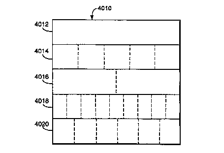
With reference to Figure 3, a module 4010, such as a ~tele-shopping module, is
a set
of resource files and data comprising the following:
a single application file 4012;
an undetermined number of graphic object description unit files 4014;
an undetermined number of variables block unit files 4016;
an undetermined number of instruction sequence files 4018; and
where appropriate, data files 4020 such as icon library files, image files,
character font files, colour table files and ASCII text files.
In the MPEG data stream, each module comprises a group of MPEG tables. Each
MPEG table may be formatted as a number of sections. In the MPEG data stream,
each section has a "size" of up to 4 kbytes. For data transfer via the serial
and
parallel port, for example, modules similarly are split into tables and
sections, the size
of the section varying with the transport medium.
Modules are transported in the MPEG data stream in the form of data packets of
typically 188 bytes within respective types of data stream, for example, video
data
streams, audio data streams and teletext data streams. Each packet is preceded
by a
Packet Identifier (PID) of 13 bits, one PID for every packet transported in
the MPEG
data stream. A programme map table (PMT table) contains a list of the
different data
streams and defines the contents of each data stream according to the
respective PID.
A PID may alert a device to the presence of applications in the data stream,
the PID
being identified using the PMT table.
Referring to Figure 4, the receiver/decoder comprises a RAM memory 4022
coupled
to a microprocessor 20 which is also coupled to a FLASH memory 4024, an
EEPROM memory 4024', and a ROM memory 4026 over a bus 21. The RAM
memory 4022 is also coupled to a DMA (direct memory access) unit 22 through
CA 02284044 1999-09-17
WO 98/43248 PCT/EP97/02112
-16-
which data (eg from an MPEG bitstream) can be entered directly into the RAM
memory.
The RAM memory is 256 kbytes long, and ~is divided into 3 areas: an area 24
which
is reserved for use by the manufacturer of the system; an area 25 which is
reserved
for use by a virtual machine (VM), and a user area 26 which is used to contain
a
variety of information such as buffers, applications 30, 30', 30", data etc.
The system
is defined by a functional specification allowing the manufacturer
considerable
freedom in designing the hardware to implement the system; the memory area 24
is
used in effect as an interface between the functions specified by the
functional
specification and the hardware. The VM in area 25 is in effect a kind of
operating
system for the computer system, and the VM and the microprocessor 20 can
together
be regarded as a run time engine (RTE) 4008. A variety of different
applications may
be loaded into the memory at different times.
Communication is necessary between the VM and the applications, and between
the
different applications themselves. This communication is handled primarily by
means
of buffers, which are common to the VM and the various applications.
Ia the present system, a command (the Set Buffers command) is used to define a
buffer area 32 in the user area 26 and the division of that buffer area into
individual
buffers. This defines a number of buffer pools; for each pool, the size of the
buffers
in the pool and the number of buffers in the pool are given. Figure 6 shows
the
logical format of the Set Buffers command. This comprises an initial entry 35
defining the number of pools NP, followed by a set of entries 36, 36',
.........., one for
each pool, with each pool entry consisting of a first sub-entry 37 defining
the pool
size PS of the pool (ie the number of buffers in the pool) and a second sub-
entry 38
defining the buffer size BS of the buffers (ie the number of bytes in the
buffers) in
the pool.
For convenience, these and other parameters used below are listed:
NP: number of pools
CA 02284044 1999-09-17
WO 98/43248 PCT/EP97/02112
-17-
per pool -
PS: pool size (number of buffers in pool)
BS: buffer size
PN: pool number
BN: buffer number (in pool)
ByN: byte number (in buffer)
In the user memory area 26, the pools of buffers are arranged sequentially
from the
beginning of that area, as shown in Figure 5. The actual layout shown is for 3
pools,
with Pool 1 consisting of 5 buffers of medium size, Pool 2 consisting of 6
buffers of
small size, and Pool 3 consisting of I buffer of large size. It will also be
noted that
each pool of buffers includes a reserved section, of 16 bytes, at its
beginning. This
section is split into a 12-byte sub-section which is available to users for
use as buffer
flags, etc, and a 4-byte sub-section which is reserved for the use of the VM.
The RTE 4008 implements a buffer manager which can be regarded as forming an
addressing path 27 between the bus 21 and the user area 26 of the RAM memory
4022. Figure 7 shows the logical organization of the buffer manager. This is
first
initialized by a Set Buffers command under the control of the microprocessor
20; it
is then used to address any desired buffer.
In the buffer manager, the sub-entries PS and BS for each pool in turn are fed
to a
multiplier 35, which forms their products PS*BS. An accumulator 36 is
initialized
with the value 64k (which represents the start address of the user area 26 of
the RAM
4022), and is fed with the succession of products PS*BS via an adder 37 which
adds
16 into each product; this 16 represents the size of the reserved section at
the start of
each pool. The accumulator 36 therefore contains, in succession, the start
addresses
of each of the buffer pools in succession. These pool start addresses are fed
to a
cumulative address register 38 in which they are stored in sequence. Also,
during
initialization, the number of pools NP is stored in a number of pools register
39, the
pool sizes are stored in a pool sizes register 40, and the buffer sizes BS are
stored in
the same sequence in a buffer size register 41.
CA 02284044 1999-09-17
WO 98/43248 PCT/EP97/02112
-18-
Following initialization, the buffers can be addressed. To address a buffer,
the desired
buffer is defined by a pool number PN for the desired pool, a buffer number BN
for
the desired buffer in that pool, and a byte number ByN for the desired byte
within that
buffer.
The pool number PN is used to select the appropriate entries for that pool
from the
cumulative register 38 and the buffer size register 40. The buffer size BS is
fed to
a multiplier 45, where it is multiplied by the buffer number BN. The resulting
product is fed to an incrementer 46 which adds 16 to the product. The output
of the
cumulative register 38 is fed to an adder 47 where,it has added to it the byte
number
ByN. The output of incrcmenter 46 is fed to an adder 48 where it is added to
the
output of adder 47. The output of adder 48 passes through a multiplexes 49 as
the
desired address; that is, the address of the desired byte of the desired
buffer of the
desired pool.
The buffer manager also includes error checking circuitry. The pool number PN
is
fed to a comparator 53 which is also fed with the number of pools NP from
register
39, to check that the selected pool number is not greater than the number of
pools;
that is, to check that the selected pool is within the buffer area. The buffer
number
BN is fed to a comparator 54 which is also fed with the output of the selected
entry
in the pool size register 40, to check that the selected buffer number is not
greater
than the number of buffers in the selected pool; that is, to check that the
selected
buffer is within the selected pool. The selected byte number is fed to a
comparator
55 which is also fed with the size of the buffers in the selected pool, to
check that the
desired byte number is not greater than the length of the buffer; that is, to
check that
the selected byte is within the selected buffer. These comparators all feed a
common
output, producing an error signal ERR if any of the checks fail.
The description so far has assumed that a buffer is being addressed. However,
it may
be desired to address the reserved or special 16-byte initial area of a pool
of buffers.
The selection between these two options is controlled by a signal N/C, which
selects
between normal buffer accesses and what may for convenience be termed buffer
CA 02284044 1999-09-17
WO 98/43248 PCT/EP97/02112
-19-
control operations. For normal accesses, buffers are selected; the reserved
initial area
of a buffer pool is only selected for control operations.
The N/C signal is fed to the multiplexer 49. For normal buffer accesses, this
signal
selects the output of adder 48, as described above. ,For control operations on
the
reserved area of a pool, however, the muitiplexer selects instead the output
of adder
47 direct. Since this path from the cumulative register 38 does not pass
through the
incrementer 46, this results in the selection of the desired byte in the
reserved area of
the pool rather than in one of the buffers following that reserved area.
For control operations on the buffer area, the comparator 55 needs to be
disabled.
This comparator is therefore enabled by the signal N/C for normal buffer
accesses and
disabled for control operations. A further comparator 56 is also fed with the
byte
number ByN and the number of bytes in the reserved pool areas, ie 16, and is
enabled
by the signal N/C for system accesses. This comparator check that the desired
byte
number is not greater than 16; that is, it checks that the selected byte is
within the
reserved area at the start of the selected pool. Obviously, this check can be
refined
to discriminate between accesses to the 12-byte sub-section which is available
to
users for use as buffer flags, etc, and the 4-byte sub-section which is
reserved for the
use of the RTE.
If desired, the Set Buffers command may also include a User Memory End
parameter
34, as shown in Figure 9, defining the end of the user memory area 2b. The
last entry
into the Set Buffers command would be stored in a suitable register, and can
be used
to check that the buffer area does not extend beyond the end of the user
memory area
26. (This is in general extremely unlikely, as space has to be left for the
applications
30, 30', 30", .............. However, it may occur if the system is designed
so that the
buffer area can be located somewhere in the middle of the user area rather
than at its
beginning as described above.)
In principle, the Set Buffers command can be used to initialize the buffer
area at any
time. Howcver, re-initializing the buffer area will effectively result in the
loss of all
*rB
CA 02284044 1999-09-17
WO 98/43248 PCT/EP97/02112
-20-
(or nearly all) the information already in the buffers, so the Set Buffers
command will
normally be executed only on system initialization.
Referring to Figure 8, the system comprises a flash memory 4024, a RAM memory
4022, and an EEPROM memory 4026 all coupled to a microprocessor 120 over a bus
12I. (Alternatively, the EEPROM memory may be coupled directly to the
microprocessor 120.) The flash memory is divided into 8 pages Pl-P8 of equal
size,
as shown in Figure 9. Of these pages, page P8 is reserved for the use of the
manufacturer; the remaining pages are free for use by the user.
Figure 9 also shows the main record table register 122 and back-up record
table
register 123, which are resident in the EEPROM 4026. The information in these
tables is in somewhat compressed and coded form. Specifically, the final
section 125
of table 122 is a CRC byte, and the section 126 before that is a page number
which
identifies the spare page. The first section 127 of table 122 consists of 6
sub-sections
127-1 to 127-6, one for each of the valid pages of the flash memory (ie the 6
pages
left apart from the spare page and the reserved page P8). These sub-sections
correspond to these remaining pages in sequence.
Figure 10 shows the logical layout of a flash memory page Pn and a sub-section
127-m of the record table and the relationship between them. (Depending on
where
the spare page is, m may equal n or n-1.)
Considering first the flash memory page, this can contain a maximum of 16
blocks of
data. The page has a header 130 which contains 16 sections, one for each
possible
data block. Each section of the header 130 contains an offset or pointer to
the start
of its data block; this pointer is in effect the address of the block within
the page.
The data blocks 131,131', ......... in the page can therefore be in any order.
Each data
block contains a respective header 132, 132', ......... which can contain a
variety of
items relating to the block, such as the name of the block, a version number,
the block
length, status information, and so on.
CA 02284044 1999-09-17
WO 98/43248 PCT/EP97/02112
-21-
The sub-section 127-m of the record table consists of lb bits, each bit being
a block
validity indicator for the corresponding section in the page header 130 as
shown.
The process of updating a page in the flash.memory will now be described. All
the
manipulations required for page updating are performed by the microprocessor
120.
First, the main record table in register 122 is checked for validity; that is,
the CRC of
sections 126 and 127 is calculated and compared to the stored CRC in section
125.
The main record table is then copied into the back-up record table register
123 (and,
if desired, the back-up record table can then be checked for validity, to
ensure that
the copying was error-free).
Next, the page being updated (the old page) is copied from the flash memory
into the
RAM memory. The sub-section 127-m in the main record table for that page is
extracted, and any data blocks marked as invalid are deleted from the page
image in
the RAM memory. The new data blocks are written into the page image.
It may be that the new data blocks will not fit easily into the spaces between
the
remaining original data blocks. These remaining blocks will in general be
separated
by blank areas of various sizes. They are therefore shifted up the page image
to
"squeeze out" the unused areas between them, effectively moving the unused
areas to
the bottom of the page image to form a single large unused area. This ensures
that
the new data blocks can be written into the page image (provided, of course,
that the
page capacity is not exceeded). The block header in the page image is of
course
updated, by changing its pointers to the new positions of the data blocks in
the page
image.
The sub-section of the record table for the page being updated was previously
extracted from the record table. That extracted sub-section is now updated, by
setting
the validity bits for any new data blocks which have been added to the page
image.
Next, the whole of section 127 of the record table is extracted from the main
record
CA 02284044 1999-09-17
WO 98/43248 PCT/EP97/02112
-22-
table register 122. The sub-section corresponding to the page being updated
(the old
page) is effectively deleted. This is the sub-section which was previously
extracted
by itself, and has been updated. This new sub-section (corresponding to the
new
page, ie the spare page into which the updated page is being written) is
inserted into
the sequence of sub-sections at the appropriate point. For this, the sub-
sections for
any pages between the old and new pages have to be shifted along to fill up
the
sub-section which has been deleted and make room for the new sub-section.
Next, the updated page image in the RAM memory is copied into the spare page,
as
identified by the spare page number in section 126 of the main record table.
Next, the page number in the spare page section is changed to the page number
of the
old page, which now becomes the new spare page.
Next, the updated record table is copied into the main record table register
122.
Finally, the updated contents of the main record table register 122 are copied
into the
back-up record table register 123, and, if desired, the contents of the main
record
table in register 122 and/or the back-up record table can be checked for
validity.
When the system is restarted, eg. after powering down, the two record tables
may both
be checked for validity; if either is found to be invalid, it can be replaced
by the valid
one (ie. the contents of the valid record table being copied into the invalid
record
table).
It will be understood that the present invention has been described above
purely by
way of example, and modifications of detail can be made within the scope of
the
invention.
Each feature disclosed in the description, and (where appropriate) the claims
and
drawings may be provided independently or in any appropriate combination.
In the aforementioned preferred embodiments, certain features of the present
invention
CA 02284044 1999-09-17
WO 98/43248 PCT/EP97/02112
-23-
have been implemented using computer software. However, it will of course be
clear
to the skilled man that any of these features may be implemented using
hardware.
Furthermore, it will be readily understood that the functions performed by the
hardware, the computer software, and suchlike are performed on or using
electrical
and like signals.
Cross reference is made to our co-pending applications, all bearing the same
filing
date, and entitled Signal Generation and Broadcasting (Attorney Reference no.
PC/ASB/19707), Smartcard for use with a Receiver of Encrypted Broadcast
Signals,
and Receiver (Attorney Reference No. PC/ASB/19708), Broadcast and Reception
System and Conditional Access System therefor (Attorney Reference No.
PC/ASB/197I0), Downloading a Computer File from a Transmitter via a
Receiver/Decoder to a Computer (Attorney Reference No. PC/ASB/19711),
Transmission and Reception of Television Programmes and Other Data (Attorney
Reference No. PC/ASB/19712), Downloading Data (Attorney Reference No.
PC/ASB/19713), Computer Memory Organisation (Attorney Reference No.
PC/ASB/19714), Television or Radio Control System Development (Attorney
Reference No. PC/ASB/19715), Extracting Data Sections from a Transmitted Data
Stream (Attorney Reference No. PC/ASB/19716), Access Control System (Attorney
Reference No. PC/ASB/19717), Data Processing System (Attorney Reference No.
PC/ASB/19718), and Broadcast and Reception System, and Receiver/Decoder and
Remote Controller therefor (Attorney Reference No. PC/ASB/19720). The
disclosures
of these documents are incorporated herein by reference. The list of
applications
includes the present application.