Note: Descriptions are shown in the official language in which they were submitted.
CA 02284851 1999-09-24
1
TECHNICAL FIELD
The present invention relates to a contour emphasizing circuit,
wherein a digital contour-emphasized video signal on the basis of the
input of an analog signal is output, and is employed to indicate
contour-emphasized color video signals by the display device (for
example, matrix type display device) of digital driving such as the
plasma display (referred only to as PDP) and liquid crystal display
(referred only to as LCD).
I~tACKGROUND ART
In the conventional CRT (Cathode Ray Tube) display device, the
contour emphasizing processing is being carried out aiming at the high
picture quality implementation and high-pass characteristic
compensation. The contour emphasizing circuit to carry out this
contour emphasizing processing is, as shown in Fig.l, composed by an
Y/C separation circuit 10, a color demodulation circuit 12, a contour
extracting circuit, phase adjustment circuits 16, 18 and 20, an adder 22
and a matrix circuit 24.
The Y/C separation circuit 10 separates an Y (luminance) signal
and a C (color) signal from the composite video signal (for example,
compound color television signal) input to an input terminal 26, and the
color modulation circuit 12 separates a Y signal, an R-Y (color
CA 02284851 1999-09-24
2
difference) signal and a B-Y (color difference) signal on the basis of a
Y signal and a C signal.
The contour extracting circuit 14 extracts the contour component
Ye which is a high-pass component of a video signal on the basis of an
adder 22.
The matrix circuit 24 prepares a signal adding the contour
component Ye to the R (red), G (green) and B (blue) signals,
respectively, on the basis of (Y+Ye) signals added by the adder 22, an
(R-Y) and a (B-Y) signal phase-adjusted by phase adjustment circuits
18 and 20. That is to say, the matrix circuit 24 prepares R+Ye, G+Ye
and B+Ye on the basis of the operations in following equations (1), (2)
and (3). By outputting these R+Ye, G+Ye and B+Ye to the CRT
display device by means of output terminals 28r, 28g and 28b, videos
contour-emphasized by this CRT display device are displayed.
(R-Y)+(Y+Ye)=R+Ye ... (1)
(G-Y)+(Y+Ye)=G+Ye ... (2)
(B-Y)+(Y+Ye)=B+Ye ... (3)
(G-Y) in the above equation (2) is generated by the following
equation (4).
In case a video contour-emphasized by the matrix type display
device driving by digital video signals (for example, R, G and B
signals) like PDP and LCD is displayed, each signal of (R+Ye), (G+Ye)
and (B+Ye) obtained in output terminals 28r, 28g and 28b in Fig.l is
output to the display device after digitized by the A/D (analog/digital)
conversion circuit. However, in such a prior example, in case a large
amplitude signal is input in an input terminal 26, or in case the contour
emphasizing quantity (or contour emphasizing coefficient, the
CA 02284851 1999-09-24
3
description is omitted, as it is similar afterwards) is "large", there is a
problem that the correct operation cannot be obtained over the dynamic
range of A/D conversion circuit.
For example, in case a large amplitude signal is input in the input
terminal 26, by outputting a signal over the dynamic range of A/D
conversion circuit as shown at the left-hand side in Fig.2(a) from output
terminals 28r, 28g and 28b, there are problems that signals exceeding an
upper conversion reference voltage value VRT (for example, 5 volts) in
the dynamic range as shown at the right-hand in said figure (a) are cut,
resulting in producing white crushing or signals under the lower
conversion reference voltage value VRT (for example, 3 volts) in the
dynamic range are cut, resulting in producing black crushing.
Further, in case the contour emphasizing quantity of the contour
extracting circuit 14 is "large", there are problems that signals over the
dynamic range of A/D conversion circuit as shown at the left-hand side
in Fig.2(b) are cut, resulting in producing white crushing or signals
under the lower conversion reference voltage value VRB are cut,
resulting in producing black crushing.
The present invention is carried out taking into account said
problems, and even when a large amplitude signal, wherein white
crushing or black crushing is input in the contour emphasizing circuit in
Fig.l, or even when the contour emphasizing quantity is "large", aims at
realizing the contour emphasizing circuit that can display a contour
emphasizing video without white crushing or black crushing in the
display device driven by a digital video signal.
CA 02284851 1999-09-24
4
DISCLOSURE O F THE INVENTION
The contour emphasizing circuit accordingthe presentinvention
to
is characterizedby being provided with an conversioncircuit
A/D to
output analog color video signals (for example, R, G and B signals) to
digital color video signals, a Y signal generation circuit to generate a Y
signal from this digital color video signal, a contour extracting circuit
to extract a contour component from the generated Y signal, and a
contour adder to output a signal contour-emphasized by adding this
extracted contour component to digital color video signals output from
the A/D conversion circuit.
Since a Y signal is generated after analog color video signals are
converted to a digital signal by the A/D conversion circuit, and the
contour component extracted from this Y signal is added for output to
digital color video signals output from the A/D conversion circuit, there
is no contour emphasizing component over the dynamic range of A/D
conversion circuit as a prior example. For this reason, in case analog
color video signals to input in the contour emphasizing circuit of the
present invention are large amplitude signals, or even in case the
contour emphasizing quantity is "large", in case a signal output from
the contour emphasizing circuit of the present invention is output to the
display device driven by a digital video signal and a contour
emphasizing video is displayed, neither white crushing nor black
crushing is produced.
Hence, to output a video signal adding a vertical contour
component and a vertical contour component and to be able to display a
video emphasizing contours in vertical direction and in horizontal
direction, the contour extracting circuit comprises first and second line
CA 02284851 1999-09-24
memories, a vertical contour extracting circuit, a contour emphasizing
frequency setting circuit, a horizontal contour extracting circuit and a
contour synthesis circuit.
Further, to simplify the circuit configuration of the contour
5 emphasizing frequency setting circuit, it comprises 1-dot delay
elements of four contour emphasizing frequency setting circuits
connected in series, a Y signal of 2-dot delay is output from the outside
side of the second 1-dot delay element, and a Y signal of 4-dot delay is
output from the output side of the fourth 1-dot delay element.
Further, to avoid a noise influence, in the contour extracting
circuit, a core ring circuit to suppress the contour component of less
than a level is set.
Further, to make the contour emphasizing quantity large, a gain
controller to output adjusting the size of the contour component
extracted in the contour extracting circuit and a coefficient
multiplication circuit to output to the contour adder by multiplying
coefficients Kr, Kg and Kb of less than to its output signal is set.
ERIEF DESCRIPTION OF THE DRAWINGS
Fig.l is a block diagram showing a contour emphasizing circuit of
prior example.
Fig.2 is to show problems in case the signal obtained in the circuit
in Fig.l is A/D converted, and output to the display device driven by a
digital video signal, and (a) is a figure, showing that white crushing and
black crushing are produced when a large amplitude signal is input, and
(b) is a figure showing that white crushing and black crushing are
produced when the contour emphasizing quantity is "large".
CA 02284851 1999-09-24
6
Fig.3 is a block diagram showing an embodiment of the contour
emphasizing circuit according to the present invention.
Fig.4 is a block diagram showing an example of the Y signal
generation circuit in Fig.3.
Fig.S is a block diagram showing an example of the contour
extracting circuit in Fig.3.
Fig.6 is a characteristic diagram of the core ring circuit in Fig.S.
Fig.7 shows the signal waveform relating to the contour emphasis
in horizontal direction, (a) is a waveform diagram of signal ~ in Fig.S,
(b) is a waveform diagram of signal ~ in Fig.S, (c) is a waveform
diagram of signal 0 in Fig.S, (d) is a waveform diagram of signal
in Fig.S and (e) is a waveform diagram of component in horizontal
direction of a signal output to an output terminal 86r in Fig.3.
Fig.8 shows a signal waveform relating to the contour emphasize in
vertical direction, (a) is a waveform diagram of signal ~ in Fig.S, (b)
is a waveform diagram of signal ~ in Fig.S, (c) is a waveform diagram
of signal ~ in Fig.S, (d) is a waveform diagram of signal ~ in Fig.S,
and (e) is a waveform diagram of component in vertical direction of a
signal output to the output terminal 86r in Fig.3.
BEST MODE TO REALIZE THE INVENTION
Below, to explain in detail the present invention, this will be
explained on the basis of the attached drawings.
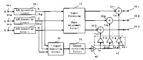
Fig.3 is to show an embodiment of the present invention. In this Fig.3,
30r, 30g and 30b are A/D conversion circuits, 32 is a signal
processing/phase adjustment circuit, 34r, 34g and 34b are contour
adders, 36 is a Y signal generation circuit, 38 is a contour extracting
CA 02284851 1999-09-24
7
circuit, 40 is a gain controller of contour component, and 42 is a
coefficient multiplication circuit.
Said A/D conversion circuits 30r, 30g and 30b are constituted,
respectively, so that the analog R, G and B signals input in the input
terminals 44r, 44g and 44b are converted for output to digital R, G and
B signals of 8-bits resolution.
Said signal processing/phase adjustment circuit 32 carries out the
signal processing like picture element number conversion, gamma
correction, etc. to the R, G and B signals output from said A/D
conversion circuits 30r, 30g and 30b, as well consists in carrying out
the phase adjustment for output to adjust the delay difference. Said
picture element number conversion denotes the processing to carry out
the sample number rate conversion of 8-bits digital R, G and B signals
to match with the displayed picture element number of the display
device, and said gamma correction processing denotes the processing to
correct the luminous characteristic of the display device. Said phase
adjustment employs a 1-dot delay element, etc. composed of a D-FF (D
type flip flop), and denotes the processing to adjust the delay difference
between the delay time required for the signal processing like said
picture element number conversion, gamma correction, etc. and the
delay time required for the signal processing in said Y signal generation
circuit 36, contour extracting circuit 38, gain controller 40 and
coefficient multiplication circuit 42.
Said Y signal generation circuit 36 is constituted so that a Y
(luminance) signal is generated from digital R, G and B signals output
from said A/D conversion circuits 30r, 30 and 30b. This Y signal
generation circuit 36 is realized by the method to obtain the
CA 02284851 1999-09-24
8
approximate value of a Y signal to satisfy the following equation 96) by
the pith addition as shown in Fig.4.
Y=(0.3 X R)+(0.59 X G)+(0.11 X B) ... (5)
Y= 0.3125 X R+0.5625 X G+0.1250 X B ... (6)
Said contour extracting circuit 38 is constituted so that the contour
component will be extracted for output from a Y signal generated in the
said Y signal generation circuit 36. This contour extracting circuit 8
is constituted concretely as shown in Fig.S.
In Fig.S, 46 denotes an input terminal of Y signal, 48 and 50 denote
first and second line memories as 1-line delay elements, 52 denotes a
vertical contour extracting circuit, 54 denotes a contour emphasizing
frequency setting circuit, 56 denotes a horizontal contour extracting
circuit, 58 denotes a gain controller of vertical contour component, 60
denotes a gain controller of horizontal contour component, 62 denotes a
contour synthesis circuit, 64 denotes a core ring circuit and 66 denotes
a gain controller.
Said first and second line memories 48 and 50 are constituted by
generating for output a Y signal input in said input terminal 46 in
generating a Y signal delayed gradually in the portion of 1 line (portion
of 1 scanning line).
Said vertical contour extracting circuit 52 comprises an adder 68
by adding for output a Y signal input in said input terminal 62 and a Y
signal of 2-line delay output from said second line memory 50, a
multiplier 70 by multiplying for output a coefficient (1/4) to an output
signal of this adder 68, a multiplier 72 by multiplying for output a
coefficient (1/2) to a Y signal of 1-line line delay output from said first
line memory 48, and a subtracter 74 subtracting an output signal of said
CA 02284851 1999-09-24
9
multiplier from an output signal of said multiplier 72.
Said contour emphasizing frequency setting circuit 54 is a circuit
to set the contour emphasizing frequency to the specified frequency (for
example, 1/2 of sampling frequency Fs), and concretely, comprises a
5-tap type composed of four 1-dot delay elements Dl through D4
delaying a Y signal output from said first line memory 48 gradually in
the portion of 1 dot (portion of 1 picture element). Said 1-dot delay
elements D1 through D4 comprise, for example, D-FF (D type flip flop),
respectively. Further, said contour emphasizing frequency setting
circuit 54 is not limited to the 5-tap type, and may be of 7-tap type
composed of six 1-dot delay elements D1 through D6 connected in
series.
Said horizontal contour extracting circuit 56 comprises a Y signal
output from said first line memory 48, an adder 76 adding a Y signal of
4-dot delay output from the fourth 1-dot delay element D4, a multiplier
80 by multiplying for output a coefficient (1/2) to a Y signal of 2-dot
delay output from the second 1-dot delay element D2, an output signal
of said coefficient device 78 from an output signal of said coefficient
device from an output signal of said coefficient device and a subtracter
82 subtracting an output signal of said coefficient device 78 from an
output signal of said coefficient device.
Said gain controller 58 has been so constituted for output by
multiplying an adjustable coefficient Kv to a vertical contour
component extracted in said vertical contour extracting circuit 52.
Said gain controller 60 has been so constituted for output by
multiplying an adjustable coefficient Kh to a vertical contour
component extracted in said vertical contour extracting circuit 56.
CA 02284851 1999-09-24
Said contour synthesis circuit 62 has been so constituted for output by
synthesizing contour components output, respectively, from said gain
controllers 58 and 60.
Said core ring circuit 64 has been, to eliminate noise and minute
5 contour components, so constituted for output by making contour
components output from said contour synthesis circuit 62 as an input,
and suppressing contour components of less than a certain level of these
contour components input. Said core ring circuit 64 has been, for
example, so constituted to possess input-output characteristics as
10 shown in Fig.6. Concretely, it has been constituted so that when
contour components input from the contour synthesis circuit 62 are
positive of larger than 0 - 8 ( 8 is a positive constant) will be added
for output to original components, and when they are negative of
smaller than 0 + 8 will be added for output to original components,
and more, when their operational results are more than - 8 and less
than + 8 the output will be fixed to 0.
Said gain controller 66 has been so constituted for output to an
output terminal 88 by multiplying an adjustable coefficient K1 to
contour components output from said core ring circuit 64.
Said gain controller 40 has been so constituted for output by
multiplying an adjustable coefficient K2 to contour components output
from said contour extracting circuit 38.
Said gain controllers 66 and 40 may omit one part (for example 66)
as the need arises.
Said coefficient multiplication circuit 42 has been constituted by
adders 84r, 84g and 84b to output contour components Yer, Yeg and Yeb
for R, G and B by multiplying coefficients Kr, Kg and Kb to the contour
CA 02284851 1999-09-24
11
component output from said gain controller 40. Said coefficients Kr,
Kg and Kb , not being limited to these, have been set to 0.3125, 0.5625
and 0.1250 of same values as coefficients (Fig.4) of R, G and B
employed so that said Y signal generation circuit 36 will generate a Y
signal.
Said contour adders 34r, 34g and 34b have been so constituted to
output to the display device through output terminals 86r, 86g and 86b,
by adding contour components Yer, Yeg and Yeb output from coefficient
devices 84r, 84g and 84b of said coefficient multiplication circuit 42 to
R, G and B signals with signal processing an phase adjustment made in
said signal processing/phase adjustment circuit 32.
Next, functions will be explained.
(1) In Fig.3, analog R, and B signals input in input terminals 44r,
44g and 44b are converted to 8-bits digital R, G and B signals by A/D
conversion circuits 30r, 30g and 30b, signal-processed and phase-
adjusted by the signal processing/phase adjustment circuit, and input to
the other input side of contour adders 34r, 34g and 34b.
(2) The Y signal generation circuit 36 generates Y signals from
digital R, G and B signals output from A/D conversion circuits 30r, 30g
and 30b. For example, this Y signal generation circuit 36 generates Y
signals from digital R, G and B signals by the bit shift addition
employing a circuit in Fig.4.
(3) The contour extracting circuit 38 extracts contour
components composed of the horizontal contour component and vertical
contour component from Y signals. Next, the extraction function of
contour components by this contour extraction circuit will be explained
employing Fig.S.
CA 02284851 1999-09-24
12
(3a) The functions to extract the horizontal contour component
will be explained referring to Fig.7.
Vertical lines S1, S2, S3, S4 and SS expressed with dotted lines in
Fig.7 express sampling points of each picture element successively in
line in horizontal direction along with scanning lines including picture
elements in the object of processing.
If a Y signal to output from the second 1-dot delay element D2 in
the contour emphasizing frequency setting circuit 54 is made ~, a
signal ~ to output from the multiplier 80 of the horizontal contour
extracting circuit 56 is made as shown in said figure (b) and is input to
the + side of the subtracter 82.
A Y signal output from the 1-line memory 48 and a Y signal output
from the fourth 1-dot delay element D4 of the contour emphasizing
frequency setting circuit 54 are added by the adder 76 of the horizontal
contour extracting circuit 56, multiplied to 1/4 by the adder 78, and
input in the - side of the subtracter as a signal ~, as shown in Fig.7(c).
Signals (~ and 0 ) operated by this subtracter 82 are multiplied Kh
times the coefficient by the gain controller, and input to the other input
side of the contour synthesis circuit 62 as a signal ~ as shown in
Fig.7.
(3b) Functions to extract the vertical contour component will be
explained referring to Fig.8.
vertical lines S1, S2 and S3 expressed by dotted lines in Fig.8 are
picture elements on three scanning lines; scanning line including
picture elements in the object of the processing and scanning lines back
and forth, and express sampling points of three picture elements along
the vertical direction including picture elements in the object of the
CA 02284851 1999-09-24
13
processing.
In case a Y signal of 1-line delay output from a first line memory
48 is made ~ as shown in Fig.8(a), a signal O output from the
multiplier 72 of the vertical contour extracting circuit 52 is made as
shown in said figure (b), and inputs in the + side of the subtracter 74.
A Y signal input in the input terminal 46 and a Y signal of 2-line delay
output from the second line memory 50 are added by the adder 68 of the
vertical contour extracting circuit 52, multiplied 1/4 by the multiplier,
and as shown in Fig.8(c), enter in the - side of the subtracter 74 as a
signal ~. Signals (+O and Q~) operated by this subtracter 74 are
multiplied Kv times the coefficient by the gain controller 58, and input
in the input side of the contour synthesis circuit 62 as a signal f1 as
shown in Fig.8(d).
(3c) A signal ~, expressing the horizontal contour component
output from the gain controller and a signal Z expressing the vertical
contour component from the gain controller 58 are synthesized by the
contour synthesis circuit 62, suppress contour components of less than a
certain level by the core ring circuit 64, eliminate a noise influence, are
level-adjusted by multiplying the coefficient K1 by the gain controller,
and output to the output terminal 88.
(4) Contour components output to the output terminal 88 are
level-adjusted by multiplying the coefficient K2 by the gain controller
40, multiplying coefficients Kr, Kg and Kb by adders 84r, 84g and 84b
of the coefficient multiplication circuit 42, become contour components
Yer, Yeg and Yeb for R, G and B, and input in another input side of
corresponding contour adders 34r, 34g and 34b. For this reason, the
contour emphasis quantity can be made large R, G and B signals
CA 02284851 1999-09-24
14
signal-processed and phase-adjusted by the signal processing/phase
adjustment circuit 32 and contour components Yer, Yeg and Yeb for R, G
and B output from adders 84r, 84g and 84b of the coefficient
multiplication circuit 42 are added by contour adders 34r, 34g and 34b,
output to the display device through output terminals 86r, 86g and 86b,
and images contour-emphasized by this display device are displayed.
At this time, components in horizontal direction of signals (R+Yeg)
to output to the output terminal 86r become as shown in Fig.7(e), and
components in vertical direction become as shown in Fig.8(e). Rh
and Rv shown by two-dot chain line in Fig.7 and Fig.8(e) express
components in horizontal direction and components in vertical direction
of R signals to output from the signal processing/phase adjustment
circuit 32.
Likewise, components in horizontal direction and components in
vertical direction of (G+Yeg) and (B+Yeb) signals to output to output
terminals 86g and 86b are made similar to components in horizontal
direction and components in vertical direction of (R+Yer) signals to
output to the output terminal 86r.
(5)As described above, since it has been designed so that a Y signal
is generated after converting analog R, G and B signals to digital R, G
and B signals by A/D conversion circuits 30r, 30g and 30b, and contour
components extracted from this Y signal is added to original digital R,
G and B signals, there are no contour emphasizing components like
prior example shown in Fig.l over dynamic ranges of A/D conversion
circuits. For this reason, analog R, G and B signals to input in the
contour emphasizing circuit of the present invention are large
amplitude signals or even in case the contour emphasis quantity is
CA 02284851 1999-09-24
"large", neither white crushing nor black crushing is produced when the
video is displayed by outputting signals to output from the contour
emphasizing circuit of the present invention to the display device (for
example, dot matrix type PDP display device) driving by digital R, G
5 and B signals.
In the embodiment shown in Fig.3, it is designed so that the
contour emphasis quantity for R, G and B will be made large by
multiplying coefficients Kr, Kg and Kb (Kr+Kg+Kb=1) of less than 1 to
the gain controller 40 to output the size of contour components
10 extracted by the contour extracting circuit 38 and its output signal, and
installing the coefficient multiplication circuit 42 to output to contour
adders 34r, 34g and 34b. The present invention is not limited to this,
can omit the gain controller 40 and coefficient multiplication circuit 42,
and can utilize also what designed to output the output of the contour
15 extracting circuit 38 directly to contour adders 34r, 34g and 34b.
In embodiments shown in Figs.3 and 5, in the contour extracting
circuit 38, a core ring circuit suppressing for output less than a certain
level of contour components output from the contour synthesis circuit
62 is installed to eliminate a noise influence, but the present invention
is not limited to this, can utilize also what omitted this core ring circuit
64.
In embodiments shown in Figs.3 and 5, it is designed so that the
contour extracting circuit 38 will be constituted by first and second line
memories 48 and 50, a vertical contour extracting circuit 52, a contour
emphasizing frequency setting circuit 54, a horizontal contour
extracting circuit 56, gain controllers 58 and 60, and a contour
synthesis circuit 62 and contour components synthesized by the vertical
CA 02284851 1999-09-24
16
contour component and horizontal contour component will be output,
however, the present invention is not limited to this, the contour
extracting circuit 38 may be provided al least with the contour
emphasizing frequency setting circuit 54 and horizontal contour
extracting circuit 56 and output horizontal contour components.
INDUSTRIAL APPLICABI rTv
As described above, the contour emphasizing circuit according to
the present invention is applicable for expressing the video of high
picture quality contour-emphasized on the basis of the input of analog
color video signals, by the display device (for example, matrix type
display device) driven by digital color video signals like PDP, LCD,
etc.