Language selection

Search

Patent 2284948 Summary

Third-party information liability

Some of the information on this Web page has been provided by external sources. The Government of Canada is not responsible for the accuracy, reliability or currency of the information supplied by external sources. Users wishing to rely upon this information should consult directly with the source of the information. Content provided by external sources is not subject to official languages, privacy and accessibility requirements.

Claims and Abstract availability

Any discrepancies in the text and image of the Claims and Abstract are due to differing posting times. Text of the Claims and Abstract are posted:

  • At the time the application is open to public inspection;
  • At the time of issue of the patent (grant).
(12) Patent: (11) CA 2284948
(54) English Title: COMPLEX PHASE-LOCKED LOOP DEMODULATOR FOR LOW-IF AND ZERO-IF RADIO RECEIVERS
(54) French Title: DEMODULATEUR A BOUCLE A VERROUILLAGE DE PHASE COMPLEXE POUR RECEPTEURS RADIO A FI BASSE OU NULLE
Status: Expired and beyond the Period of Reversal
Bibliographic Data
(51) International Patent Classification (IPC):
  • H04L 27/152 (2006.01)
  • H04L 27/38 (2006.01)
(72) Inventors :
  • BIRKETT, NEIL (Canada)
  • FILIOL, NORM (Canada)
  • RILEY, THOMAS (Canada)
(73) Owners :
  • SKYWORKS SOLUTIONS, INC.
(71) Applicants :
  • SKYWORKS SOLUTIONS, INC. (United States of America)
(74) Agent: GOWLING WLG (CANADA) LLP
(74) Associate agent:
(45) Issued: 2003-12-09
(22) Filed Date: 1999-10-04
(41) Open to Public Inspection: 2001-04-04
Examination requested: 1999-11-12
Availability of licence: N/A
Dedicated to the Public: N/A
(25) Language of filing: English

Patent Cooperation Treaty (PCT): No

(30) Application Priority Data: None

Abstracts

English Abstract


A digital demodulator which coherently demodulates a low-IF or zero-IF complex
signal using a complex-valued phase-locked loop (CPPL). The CPPL includes a
numerical controlled oscillator, four multipliers and two combiners to provide
independent phase/frequency and amplitude outputs. The CPLL exhibits in first
order
PLL dynamics without a loop filter in the feedback loop to the NCO. However a
filter
with one or more poles may be included in the feedback circuit to exhibit 2 nd
or higher
order PLL dynamics. The CPLL allows coherent demodulation of extremely low FM
modulation indexes whereby the incoming frequency drift may be larger than the
frequency deviation. It can also be used to coherently demodulate signals
which have
combined amplitude and phase characteristics.


Claims

Note: Claims are shown in the official language in which they were submitted.

7
What is claimed is:
1. A complex demodulator for demodulating a received RF signal converted to
digital I and Q IF signals comprising:
- a numerically controlled oscillator (NCO) for generating first and second
output signals in quadrature centred at the IF frequency;
- a first digital multiplier having a first input for receiving the digital I
IF
signal, a second input for receiving the first NCO output signal and an
output;
- a second digital multiplier having a first input for receiving the digital Q
IF signal, a second input for receiving the second NCO output signal and
an output; and
- difference combiner means coupled to the first and second digital
multiplier outputs for providing a phase signal at its output, the phase
signal being coupled to the NCO through a feedback loop to control the
NCO frequency.
2. A demodulator as claimed in claim 1 wherein the NCO first output signal is
a sine
signal and the NCO second output signal is a cos signal.
3. A demodulator as claimed in claim 2 which further includes a loop filter in
the
feedback loop between the output of the difference combiner means and the
NCO.
4. A demodulator as claimed in claim 3 wherein the filter is a single pole
filter to
produce a second order loop.

8
5. A demodulator as claimed in claim 3 wherein the filter is a two or more
pole filter
to produce a third or higher order loop.
6. A demodulator as claimed in claim 1 wherein the demodulator further
comprises:
- a third digital multiplier having a first input for receiving the digital I
IF
signal, a second input for receiving the second NCO output signal and an
output;
- a fourth digital multiplier having a first input for receiving the digital Q
IF signal, a second input for receiving the first NCO output signal and an
output; and
- sum combiner means coupled to the outputs of the third and fourth
digital multiplier outputs for providing an amplitude signal at its output.
7. A demodulator as claimed in claim 6 wherein the NCO first output signal is
a sine
signal and the NCO second output signal is a cos signal.
8. A demodulator as claimed in claim 7 which further includes a loop filter in
the
feedback loop between the output of the difference combiner means and the
NCO.
9. A demodulator as claimed in claim 8 wherein the filter is a single pole
filter to
produce a second order loop.
10. A demodulator as claimed in claim 8 wherein the filter is a two or more
pole filter
to produce a third or higher order loop.

Description

Note: Descriptions are shown in the official language in which they were submitted.


CA 02284948 1999-10-04
1
Complex Phase-Locked Loop Demodulator for Low-IF and Zero-IF Radio
Receivers
Field of the Invention
The invention relates generally to phased-locked loop demodulators, and more
particularly to a complex digital phase-locked loop demodulator.
Background of the Invention
Phase-locked loop demodulators that are capable of demodulating low IF signals
are presently available. These devices convert the RF carrier to the I and Q
quadrature
components at low IF which are processed in a phase-locked loop. An example of
such
a demodulator is described in US Patent 4,852,123 which issued on July 25,
1989 to
Bickley et al.
These demodulators are generally unstable as the IF nears zero-IF. In
addition,
these circuits which include loop filters as well as a voltage controlled
oscillator with
further filters and mixers to drive the phase-locked loop, are quite
complicated.
Therefore, there is a need for a simpler coherent FM demodulator in low-IF or
zero-IF for radio receiver architectures. In addition, it is desirable to
coherently
demodulate FM signals with extremely low modulation indexes and significant
centre
frequency offset even when such offsets are several times greater than the
maximum FM
modulation deviation.

CA 02284948 1999-10-04
2
Summary of the Invention
The invention is directed to a complex demodulator for demodulating a received
RF signal converted to digital I and Q components of the IF signal comprising
a
numerically controlled oscillator (NCO), four digital multipliers each having
a first input,
a second input and an output, a difference combiner and a summing combiner
that are
formed into a complex phase locked loop. The numerically controlled oscillator
(NCO)
generate first and second output signals that are in quadrature and centred at
the IF
frequency. The digital I IF signal is coupled to the first input of each of
the first and
third multipliers and the digital Q IF signal is coupled to the first input of
each of the
second and fourth multipliers. The first NCO output signal is coupled to the
second input
of the first and fourth multipliers while the second NCO output signal is
coupled second
input of the second and third multipliers. The outputs of the first and second
multipliers
are coupled to the difference combiner to provide a phase output while the
outputs of the
third and fourth multipliers are coupled to the summing combiner to provide an
amplitude output. The phase output is also coupled through a feedback loop to
the NCO.
In accordance with another aspect of the invention, the complex demodulator
may
further include a loop filter in the feedback loop between the output of the
difference
combiner and the NCO. The filter may be a single pole filter to produce a
second order
loop or have two or more poles to produce a third or higher order loop.
Regarding another aspect of the invention, the NCO first output signal may be
a
sine signal and the NCO second output signal may be cos signal.
Other aspects and advantages of the invention, as well as the structure and
operation of various embodiments of the invention, will become apparent to
those
ordinarily skilled in the art upon review of the following description of the
invention in
conjunction with the accompanying drawings.

CA 02284948 1999-10-04
3
Brief Description of the Drawing
The invention will be described with reference to the accompanying drawings,
wherein:
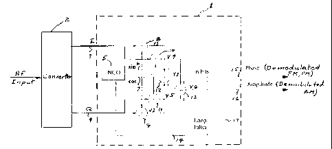
FIG. 1 is complex digital phase locked loop demodulator in accordance with
this
invention.
Detailed Description of the Invention
The complex demodulator 1 in accordance with the present invention is
illustrated
in figure 1. Connected to the demodulator 1 is a conversion circuit 2 which
receives the
input RF signal and converts it to an IF signal in the form of digital in-
phase I and
quadrature Q components, these components are applied to the demodulator 1 on
lines 3
and 4.
The conversion circuit 2 may take any conventional form such as by applying
the
input RF signal to two local oscillator mixers which are further inputted by
two local
oscillator signals that are in quadrature. The outputs from the local
oscillator mixers are
coupled to two analog to digital converters (ADC) to produce the digital I and
Q IF
signals. In an alternate system, the RF signal is converted to an analog IF
signal by an
analog mixer and filter and then the IF signal is converted by an ADC to a
digital IF
signal. The digital IF signal is then applied to a pair of digital multipliers
which will
produce the digital I and Q IF signals when oscillator signals in quadrature
are applied
to the digital multipliers.
The demodulator 1 in accordance with the present invention includes a
numerically controlled oscillator 5 , also known as a direct digital
synthesizer which
generates a pair of signals that are in quadrature on its outputs 6 and 7. The
fundamentals
of direct digital synthesizers are described in the manual "Frequency
Synthesizer Design
Handbook" by James A. Crawford published by Artech House, Inc. in 1994 - ISBN
0-89006-440-7, section 7.3, pp 308 - 343. The centre frequency of the
quadrature signals

CA 02284948 1999-10-04
4
is at the same frequency as the IF signals applied to lines 3 and 4. The
demodulator 1
further includes a first digital multiplier 8 with a first input coupled to
line 3 and a second
input coupled to line 6, a second digital multiplier 9 with a first input
coupled to line 4
and a second input coupled to line 7, a third digital multiplier 10 with a
first input
coupled to line 3 and a second input coupled to line 7, and a fourth digital
multiplier 11
with a first input coupled to line 4 and a second input coupled to line 6. The
outputs V 1
and V2 of multipliers 8 and 9 are coupled to a digital differential combiner
12 which will
provide an output signal V3 equal to the difference between its input signals
V 1 and V2.
The signal V3 represents variations in phase and thus the demodulated FM or
PM.
Further, the outputs V4 and VS of multipliers 10 and 11 are coupled to a
digital summing
combiner 13 which will provide an output signal V6 equal to the sum between
its input
signals V4 and V5. The signal V6 represents variations in amplitude and thus
the
demodulated AM. The output signal V3 is also coupled to control NCO 5 through
a
feedback loop 14.
In operation, the received RF information signal will be converted to digital
I and
Q components at IF by converter 2 preserving the information on the signal.
One
characteristic of the demodulator 1 in accordance with the present invention
is that it is
capable of demodulating a low-IF signal whether the frequency is positive or
negative
as well as a zero-IF signal.
The I component of the IF signal is multiplied by the NCO 5 sine signal and
the
Q component is multiplied by the NCO 5 cos signal producing signals V 1 and
V2. V 1
and V2 are subtracted from one another in the difference combiner 12 and
provide, at
output 15, the phase output V3 of the RF signal. In addition, the signal V3 is
used to
control the NCO through feed back loop 14. The feedback loop exhibits 1 S'
order loop
characteristics because of the properties of the NCO 5. However, if it is
desired to create
2°a, 3a or higher order feedback loops for the NCO 5, a single-pole,
two-pole or more
filter 17 can be inserted into the feedback loop 14.

CA 02284948 1999-10-04
In addition, the I component of the IF signal is multiplied by the NCO 5 cos
signal and the Q component is multiplied by the NCO 5 sine signal producing
signals V4
and V5. V4 and VS are summed in combiner 13 to provide the amplitude component
V6 of the RF information signal at output 16.
The advantages of the all digital phase-locked loop demodulator 1 in
accordance
with the present invention are numerous. Because of its coherence, the NCO
will lock
to the incoming frequency with little consequence to the demodulation
efficiency even
if the inputs are at a non-ideal frequency offset.
The demodulator 1 provides an amplitude V6 which is independent of the phase
output V3. It is the demodulated AM signal and can be used for a received
signal
strength indicator (RSSI). Demodulator 1 also provides a phase output V3 which
is the
demodulated FM or PM signal. For high loop gains, the phase response output of
the
CPLL demodulator 1 approaches that of an ideal FM discriminator and is
therefore
attractive at both low and high modulation indexes. Because the outputs V3 and
V6 are
independent of one another, the circuit may be used as an AM demodulator or FM
demodulator, or it can be used to demodulate signals which have combined
amplitude
and phase characteristics as for example a quadrature modulated signal (QAM).
In addition, the CPLL demodulator 1 is unconditionally stable; it has an
acquisition range equivalent to the loop gain since there is no need for a
loop filter. Pull-
in time will be equivalent to the first order PLL, i.e. phase lock will occur
without cycle
slipping. It has a fast acquisition time which is inversely proportional to
the loop gain;
as a result the CPLL demodulator 1 in accordance with the present invention is
attractive
for applications that demand fast acquisition times.
In addition, the CPLL demodulator 1 can track a signal even if it goes through
zero frequency. Thus it will provide both phase and amplitude information as
the signal
goes through zero frequency.

CA 02284948 1999-10-04
6
While the invention has been described according to what is presently
considered
to be the most practical and preferred embodiments, it must be understood that
the
invention is not limited to the disclosed embodiments. Those ordinarily
skilled in the art
will understand that various modifications and equivalent structures and
functions may
be made without departing from the spirit and scope of the invention as
defined in the
claims. Therefore, the invention as defined in the claims must be accorded the
broadest
possible interpretation so as to encompass all such modifications and
equivalent
structures and functions.

Representative Drawing
A single figure which represents the drawing illustrating the invention.
Administrative Status

2024-08-01:As part of the Next Generation Patents (NGP) transition, the Canadian Patents Database (CPD) now contains a more detailed Event History, which replicates the Event Log of our new back-office solution.

Please note that "Inactive:" events refers to events no longer in use in our new back-office solution.

For a clearer understanding of the status of the application/patent presented on this page, the site Disclaimer , as well as the definitions for Patent , Event History , Maintenance Fee  and Payment History  should be consulted.

Event History

Description Date
Inactive: IPC removed 2014-10-02
Time Limit for Reversal Expired 2008-10-06
Letter Sent 2007-10-04
Inactive: IPC from MCD 2006-03-12
Grant by Issuance 2003-12-09
Inactive: Cover page published 2003-12-08
Letter Sent 2003-08-08
Inactive: Correspondence - Transfer 2003-06-30
Pre-grant 2003-06-30
Inactive: Final fee received 2003-06-30
Notice of Allowance is Issued 2002-12-31
Letter Sent 2002-12-31
Inactive: Office letter 2002-12-18
Inactive: Approved for allowance (AFA) 2002-11-25
Application Published (Open to Public Inspection) 2001-04-04
Inactive: Cover page published 2001-04-03
Letter Sent 2000-06-28
Inactive: Multiple transfers 2000-05-23
Letter Sent 1999-11-30
Inactive: First IPC assigned 1999-11-19
All Requirements for Examination Determined Compliant 1999-11-12
Request for Examination Requirements Determined Compliant 1999-11-12
Request for Examination Received 1999-11-12
Letter Sent 1999-10-28
Inactive: Filing certificate - No RFE (English) 1999-10-28
Filing Requirements Determined Compliant 1999-10-28
Application Received - Regular National 1999-10-26

Abandonment History

There is no abandonment history.

Maintenance Fee

The last payment was received on 2003-09-23

Note : If the full payment has not been received on or before the date indicated, a further fee may be required which may be one of the following

  • the reinstatement fee;
  • the late payment fee; or
  • additional fee to reverse deemed expiry.

Please refer to the CIPO Patent Fees web page to see all current fee amounts.

Owners on Record

Note: Records showing the ownership history in alphabetical order.

Current Owners on Record
SKYWORKS SOLUTIONS, INC.
Past Owners on Record
NEIL BIRKETT
NORM FILIOL
THOMAS RILEY
Past Owners that do not appear in the "Owners on Record" listing will appear in other documentation within the application.
Documents

To view selected files, please enter reCAPTCHA code :


To view images, click a link in the Document Description column. To download the documents, select one or more checkboxes in the first column and then click the "Download Selected in PDF format (Zip Archive)" or the "Download Selected as Single PDF" button.

List of published and non-published patent-specific documents on the CPD .

If you have any difficulty accessing content, you can call the Client Service Centre at 1-866-997-1936 or send them an e-mail at CIPO Client Service Centre.


Document
Description 
Date
(yyyy-mm-dd) 
Number of pages   Size of Image (KB) 
Representative drawing 2001-03-20 1 7
Representative drawing 2003-11-07 1 7
Cover Page 2003-11-07 1 39
Cover Page 2001-03-20 1 37
Description 1999-10-04 6 239
Abstract 1999-10-04 1 21
Drawings 1999-10-04 1 14
Claims 1999-10-04 2 60
Acknowledgement of Request for Examination 1999-11-30 1 179
Courtesy - Certificate of registration (related document(s)) 1999-10-28 1 115
Filing Certificate (English) 1999-10-28 1 164
Reminder of maintenance fee due 2001-06-05 1 112
Commissioner's Notice - Application Found Allowable 2002-12-31 1 160
Maintenance Fee Notice 2007-11-15 1 171
Correspondence 2000-06-28 1 23
Correspondence 2002-12-19 1 18
Correspondence 2003-06-30 2 45
Fees 2002-09-26 1 28