Note: Descriptions are shown in the official language in which they were submitted.
CA 02285128 1999-11-18
1
SWITCH FOR OPTICAL SIGNALS
Field of the Invention
This invention relates to optical switches and is particularly
concerned with switches for switching optical signals composed of light
of predetermined wavelengths, for example, Dense Wavelength Division
Multiplexed (DWDM) optical signals used in optical telecommunications.
Background of the Invention
Optical transmission systems achieve their end-to-end
connectivity by concatenating multiple spans between intermediate
switching nodes to achieve an overall end-to-end path. When the end-to-
end granularity of any given transmission path is a fraction of the capacity
of a given optical carrier, time division multiplexing is used to share the
overall bandwidth, mandating the use of electronic switching in the
intermediate nodes. However the availability of Dense Wavelength
Division Multiplexing (DWDM), combined with the availability of high
capacity ports on data switches and routers, increases the demand for
concatenation of individual spans to make end-to-end connections at the
wavelength level.
DWDM optical networks transmit multiple channel signals on
each optical fiber; each channel signal being modulated light of a
predetermined wavelength allocated only to that signal. The resultant
plurality of optical carriers on each fiber, each carrying a traffic signal,
are
separated from each other in optical wavelength. Current DWDM optical
networks typically convert channel signals into electrical signals at every
switching node in the network because optical switches having a large
enough port count are not available. To convert the channel signals to
electrical signals, transponders are used at each port and for every
channel wavelength that requires conversion. As DWDM signals become
denser, that is, as the number of channels per optical fiber increases, the
required accuracy of the transponders, and hence the cost, also increases.
Moreover, as the number of ports per switching node increases, the
required number of transponders also increases. Consequently, large
networks carrying dense DWDM signals require many costly transponders
and are therefore costly to build.
To overcome this problem it has been proposed to build large,
purely optical switches in various forms, to reduce or eliminate the need
CA 02285128 1999-11-18
2
for opto-electronic conversion in order to switch channel signals
electrically. Most effort has gone into conceiving methods of building very
large switches that offer full connectivity between all their ports.
However, fabrication of these large optical switches has proven difficult.
Most attempts to create a large non-blocking optical switch
use a large number of small switch modules to create a multiple stage
switch. One example of this, envisages building a 128 port x 128 port
switch out of three stages of multiple 16 x 16 crosspoint matrices, or a
512 x 512 port switch out of three stages of multiple 32 x 32 crosspoint
io matrices, in a three stage CLOS architecture. The above is based on the
availability of 16 x 16 or 32 x 32 switch matrices in the form of Micro-
Electro-Mechanical (MEM) switch matrices (e.g."Free-space Micromachined
Optical-Switching Technologies and Architectures", Lih Y. Lin, AT&T
Labs-Research, OFC99 Session W14-1, Feb. 24, 1999). Other multi-stage
approaches use smaller matrices and more stages. Even the 3 stage CLOS
architecture is limited to 512 switched wavelengths, which, in today's
160 wavelength per fiber DWDM environment, is only adequate to handle
the output/input to 3 fiber pairs (480 wavelengths).
Such multi-stage switches, even at three stages, have
significant problems. These problems include high overall optical loss
through the switch, since the losses in each stage are additive across the
switch, and there is the potential for additional loss in the complex
internal interconnect between the stages of the switch. The size
limitations (number of wavelengths switched) can be overcome by going
to a five stage CLOS switch, but this further increases the loss through
the switch as well as adding to the complexity and cost. One of the major
cost-centres is the cost of the MEMs switch modules (or other small
matrix modules). The sensitivity of the overall switch cost to the cost of
the MEMS modules is exacerbated by the fact that a CLOS switch
3o requires a degree of dilation (extra switch paths) to be non-blocking and
that each optical path has to transit three (or five) individual modules in
series.
These prior art approaches, as well as many other variants on
various themes, attempt to generate large, general purpose, non-blocking
switches, which are then coupled to DWDM multiplexers for coupling into
output fibers. This results in substantial waste of the capacity and
capability of the non-blocking generic switches, since the DWDM
multiplexers are themselves blocking elements on all their ports to any
CA 02285128 1999-11-18
3
optical carrier except an optical carrier within the specific passband of
that port of the multiplexer. Hence the non-blocking switch structure
contains many crosspoints that direct specific input ports carrying a given
wavelength to output ports that cannot support that wavelength, since it
would be blocked in the WDM multiplexer. Such crosspoints cannot be
used in operation of the switch, and this wasting of crosspoints makes
inefficient use of expensive optical switching matrices.
Optical transmission networks that rely on electrical switching
and electrical regeneration at intermediate nodes require one pair of
to transponders per wavelength channel at each intermediate switching
node. Consequently, as the number of wavelength channels per fiber
grows, the number of transponders and the resulting costs grow in
proportion to the number of wavelength channels.
Optical transmission networks that rely on "opaque" optical
switching and electrical regeneration at intermediate nodes experience the
same growth in transponder number and cost. (In "opaque" optical
switching, incoming optical signals are converted by transponders into
different optical signals that are switched optically before being converted
by further transponders to different optical signals for further
transmission.)
However, in optically switched networks that use cascaded
optical amplifiers to compensate for fiber loss on each span and for
optical insertion loss of the optical switches, each optical amplifier
simultaneously amplifies all wavelength channels on each fiber without
the use of transponders. Consequently, the number and cost of the
optical amplifiers does not grow with the number of wavelength channels
per fiber, and the cost benefits of optically switched and amplified
networks relative to electrically switched and regenerated networks
increases with the number of wavelength channels per fiber.
Moreover, the cost advantages of optically switched and
amplified networks over electrically switched and regenerated networks
grow even faster as the maximum distance between electrical
regeneration points grows, because optically switched and amplified
networks can benefit from that increased optical reach by eliminating
transponders. In contrast, electrically switched networks require a pair of
transponders per wavelength channel at each intermediate switching point
even if the optical range exceeds the distance between switching points.
CA 02285128 1999-11-18
4
Consequently, there is a substantial advantage in designing
optical transmission networks such that the majority of wavelength
channels can be routed end-to-end via optical switches and optical
amplifiers, without the use of transponders on a per wavelength channel
basis. This leads to a need, previously unaddressed, for an optical cross-
connect switch optimized for routing wavelengths from end-to-end (as
opposed to a large opaque optical switching fabric designed to be located
between banks of transponders).
to Summary of Invention
This invention aims to provide an improved cross-connect switch which
is well-adapted for application to high capacity Wavelength Division
Multiplexed (WDM) and Dense WDM (DWDM) transmission networks.
A first aspect of the invention provides a cross-connect switch
comprising a plurality of switching matrices and a wavelength-converting inter-
matrix switch. Each switching matrix has multiple input ports and multiple
output ports. Each switching matrix is operable to switch optical channel
signals arriving on any input port to any of a plurality of the output ports.
The
multiple input ports include at least one inter-matrix input port, and the
multiple output ports include at least one inter-matrix output port. Each
switching matrix is operable to switch optical channel signals having a
respective distinct wavelength. The wavelength-converting inter-matrix switch
is connected between the inter-matrix output ports of the switching matrices
and the inter-matrix input ports of the switching matrices. The inter-matrix
switch is operable to switch a signal arriving from any inter-matrix output
port
of any switching matrix to an inter-matrix input port of any of a plurality of
other switching matrices. In switching a first channel signal having a first
wavelength from an inter-matrix output port of a first switching matrix to an
inter-matrix port of a second switching matrix, the wavelength-converting
inter-matrix switch is operable to convert the first channel signal having the
first wavelength to a second channel signal having a second wavelength.
In most practical cross-connect switches, each switching matrix is
operable to switch a signal arriving on any input port to any or substantially
any of the output ports.
CA 02285128 1999-11-18
In most practical cross-connect switches, each inter-matrix switch is
operable to switch a signal arriving from any inter-matrix output port of any
switching matrix to an inter-matrix input port of any or substantially any of
the
other switching matrices.
5 This arrangement enables the assignment of each switching matrix to a
respective wavelength of a WDM system. Channels having a particular
wavelength can be routed through the cross-connect switch in the switching
matrix assigned to that respective wavelength. Because this routing is
through a single optical switching matrix, the optical loss can be relatively
low.
to When a wavelength channel having the same wavelength is not available on
the next span of an end-to-end path, a channel having a first wavelength can
be cross-connected to channel having a second wavelength by routing the
channel at the first wavelength through the switching matrix assigned to the
first wavelength to an inter-matrix output port. The channel at the first
wavelength is routed from the inter-matrix output port of a first switching
matrix (which is assigned to the first wavelength) to the wavelength-
converting
switch where the channel at the first wavelength is connected to the channel
at the second wavelength (the signal on the channel at the first wavelength
being converted to a signal at the second wavelength). The channel at the
second wavelength is routed to an inter-matrix input port of the switching
matrix assigned to the second wavelength which completes the routing
through the cross-connect switch to a selected output port.
Each switching matrix may have multiple inter-matrix output ports, and
the wavelength-converting inter-matrix switch may comprise multiple
switching elements connected in parallel. In this case, each inter-matrix
output port of a particular switching matrix may be coupled to a respective
one
of the switching elements of the wavelength-converting inter-matrix switch.
This arrangement provides multiple paths for routing a signal from one
switching matrix through the inter-matrix switch to another switching matrix,
thereby reducing potential for blocking in the inter-matrix switch.
The inter-matrix switch may comprise at least one "add" input port and
at least one "drop" output port. In this case, the inter-matrix switch is
operable
to couple an "add" input signal arriving at the "add" input port to an inter-
matrix
input port of any switching matrix, and to couple a signal arriving from an
CA 02285128 1999-11-18
6
inter-matrix output port of any switching matrix to the "drop" output port.
These features enable the cross-connect switch to "add" signals (i.e. to
insert
traffic signals at the cross-connect switch) and "drop" signals (i.e. extract
traffic signals at the cross-connect switch) in addition to routing through
signals.
The cross-connect switch may further comprise a plurality of
wavelength division demultiplexers and a plurality of wavelength division
multiplexers. Each demultiplexer is operable to separate an optical input
signal into a plurality of output channel signals having respective distinct
lo wavelengths. The demultiplexer applies each output channel signal to a
respective input port of a respective switching matrix such that each
switching
matrix receives only channel signals having a respective distinct wavelength.
Each multiplexer has a plurality of inputs, each respective input of each
multiplexer being coupled to an output port of a respective switching matrix
to
receive a respective channel signal having a respective wavelength. Each
multiplexer is operable to combine channel signals having distinct
wavelengths into an optical output signal.
Such wavelength division demultiplexers and wavelength division
multiplexers are normally associated with the cross-connect switch and may
2o be packaged as part of the cross-connect switch. The demultiplexer receives
an optical signal comprising multiple channel signals, each channel signal
comprising an optical carrier at a respective distinct wavelength having a
respective traffic signal modulated on the carrier signal. The demultiplexer
separates the channel signals onto respective outputs for coupling to the
switching matrices, each switching matrix receiving only channel signals at
one of the distinct wavelengths. The multiplexer receives multiple channel
signals, each having a different respective wavelength from respective
switching matrices and combines the multiple channel signals for transmission
on a single output fiber.
In this arrangement, every cross-point of every switching matrix is
usable, i.e. none of the cross-points route channels at a particular
wavelength
to a WDM multiplexer port that is unable to pass signals at that wavelength.
The wavelength-converting switch may comprise multiple optical
receivers, multiple optical transmitters and an electrical switch connected
CA 02285128 1999-11-18
7
between the optical receivers and the optical transmitters. The optical
receivers are coupled to inter-matrix output ports of the switching matrices,
and are operable to convert channel signals arriving from the inter-matrix
output ports to electrical signals. The electrical switch is operable to
switch
electrical signals from any optical receiver to a plurality of the optical
transmitters. The optical transmitters are operable to convert electrical
signals to channel signals having predetermined wavelengths.
In most practical cross-connect switches, the electrical switch is
operable to switch electrical signals from any optical receiver to any or
to substantially any optical transmitter. The electrical switch may be a
single
electrical switching element or multiple electrical switching elements
connected in series or in parallel.
In this arrangement, the electrical switch is used to couple a receiver
connected to a switching matrix assigned to a first wavelength to a
transmitter
operating at a second wavelength and connected to a switching matrix
assigned to the second wavelength, thereby cross-connecting a channel
operating at the first wavelength to a channel operating at the second
wavelength.
Alternatively, the wavelength-converting switch may comprise an
optical switch, and a plurality of optical transponders connected to the
switch.
Each optical transponder is operable to convert a channel signal having a
first
wavelength into a channel signal having a second wavelength. The optical
switch is operable to couple a channel signal arriving from an inter-matrix
output port of any switching matrix to an inter-matrix input port of any of a
plurality of other switching matrices via an optical transponder.
The optical transponder may be a device having a receive half for
recovering an information signal from the incoming wavelength channel, and a
transmit half, having means to modulate the recovered information signal onto
a light source of a specific, fixed or tunable, wavelength for output on a
3o different wavelength channel. The optical switch may comprise a single
optical switching element or multiple optical switching elements connected in
series or in parallel for load sharing.
In most practical cross-connect switches, the optical switch is operable
to couple a channel signal arriving from an inter-matrix output port of any
CA 02285128 1999-11-18
8
switching matrix to an inter-matrix input port of any or substantially any
other
switching matrix.
The optical switch may be coupled between the inter-matrix output
ports and the optical transponders. In this arrangement, the optical switch is
used to couple a first channel operating at a first wavelength to a selected
transponder that converts the signal on the first channel to a signal at a
second wavelength. The transponder is connected to an inter-matrix input
port of the switching matrix that is assigned to the second wavelength.
Alternatively, the optical switch may comprise plural optical switching
io stages and the optical transponders may be coupled between optical
switching stages. For example, the optical switch may comprise a multistage
optical CLOS switch. The relatively high insertion loss of a multistage
optical
switch is acceptable in the inter-matrix switch because the inter-matrix
switch
includes transponders that restore the optical signal level as they convert an
optical signal at one wavelength to an optical signal at another wavelength.
However attention must be paid to an overall system loss budget to keep all
components operating within their specified range.
Some or all of the optical transponders may be tunable to transmit
channel signals of selectable distinct wavelengths. The use of tunable
transponders reduces the number of transponders that need to be provided to
allow for all possible wavelength conversion possibilities. Each tunable
transponder can be provisioned remotely for any of a number of wavelength
channels without requiring a visit to the switching site to physically
provision a
wavelength channel. It can be demonstrated statistically that a number of
tunable transponders can provide more combinations of channel
configurations than the same number of fixed wavelength transponders.
Moreover, the use of tunable transponders reduces the number of different
transponder types that must be stocked and inventoried.
However, tunable transponders are more expensive than fixed
wavelength transponders and currently have limited tuning range.
Consequently, some or all of the transponders may be fixed wavelength
transponders that are operable to transmit channel signals of a single
wavelength. Alternatively the tunable transponders may be arranged in
CA 02285128 1999-11-18
9
groups, each group covering the ports associated with a specific wavelength
band.
Another aspect of the invention provides an optical switching matrix
comprising first and second pairs of switching elements and a plurality of
optical combiners. Each pair of switching elements comprises a first
switching element and a second switching element. Each switching element
comprises a rectangular substrate having a plurality of input ports on a first
side, a first plurality of output ports on a second side opposite the first
side
and a second plurality of output ports on a third side adjacent the first side
to and the second side Each switching element further comprises a plurality of
optical diverters aligned between each input port and a corresponding output
port on the second side. Each diverter is aligned with a respective output
port
on the third side and is movable from a first position, in which the diverter
allows an optical signal incident from the input port to propagate in a
direction
is toward the respective output port on the second side, to a second position,
in
which the diverter diverts an optical signal incident from the input port
toward
a respective output port on the third side. For each of the first and second
pairs of switching elements, each input port of the second optical switching
element is optically coupled to a respective output port of the first optical
20 switching matrix. Each combiner is coupled to a respective output port of
the
first pair of optical switching elements and to a respective output port of
the
second pair of optical switching elements.
Construction of larger switching matrices by assembly of smaller
switching matrices as described above, may be attractive until switching
25 matrices of the desired port count are readily available at attractive
prices.
Moreover, the ability to assemble larger switching matrices from smaller
switching matrices enables modular construction of cross-connect switches so
that the size of the switch (and its installed cost) can grow gracefully with
capacity demands.
30 Another aspect of the invention provides a wavelength-converting
switch comprising an optical switch and a plurality of optical transponders
connected to the switch. Each optical transponder is operable to convert a
channel signal having a first wavelength into a channel signal having a
second wavelength. The optical switch is operable to couple a channel
CA 02285128 1999-11-18
signal arriving from an inter-matrix output port of any switching matrix to an
inter-matrix input port of any of a plurality of other switching matrices via
an
optical transponder.
The wavelength-converting switch can be used in the construction of
5 some embodiments of the cross-connect switch described above.
Another aspect of the invention provides a switching fabric for an
optical cross-connect switch. The switching fabric comprises a plurality of
optical switching matrices. Each switching matrix has multiple inter-node
input ports and at least one intra-node input port for receiving incoming
optical
io channel signals, the incoming optical channel signals having a wavelength
that is particular to that particular switching matrix. Each switching matrix
also
has multiple through output ports and at least one intra-node output port.
Each switching matrix is operable to switch optical channel signals arriving
on
any input port to any of a plurality of the through output ports and the intra-
is node output port.
In most practical switching fabrics, each switching matrix will operable
to switch optical channel signals arriving on any input port to any or
substantially any of the output ports.
The switching fabric may further comprise an add/drop multiplexer
coupled to the intra-node input port and intra-node output port of each
switching matrix. The add/drop multiplexer is operable to couple, to the intra-
node input port of any switching matrix of the plurality of switching
matrices,
optical channel signals having the wavelength that is particular to that
switching matrix. The add/drop multiplexer is also operable to receive, from
the intra-node output port of any switching matrix of the plurality of
switching
matrices, optical channel signals having the wavelength that is particular to
that switching matrix.
Another aspect of the invention provides a method of cross-connecting
optical channel signals at an optical cross-connect switch comprising a
plurality of switching matrices. The method comprises coupling each optical
channel signal having a particular wavelength to an input port of a particular
switching matrix assigned to that particular wavelength, and switching the
optical channel signal in the particular switching matrix to an output port
selected according to a desired cross-connection of the optical channel
signal.
CA 02285128 1999-11-18
11
The optical channel signal may be switched to an inter-node output
port of the particular switching matrix when the optical channel signal is to
be
cross-connected to an optical channel having the same particular wavelength.
The optical channel signal may be switched to an intra-node output
port of the particular switching matrix when the optical channel signal is to
be
cross-connected to an optical channel having a wavelength other than the
particular wavelength of the optical signal. In this case, the optical signal
may
be coupled from the intra-node output port to a wavelength converter for
conversion to an optical channel signal having another wavelength. The
io optical signal at the other wavelength can be coupled to an intra-node
input
port of another switching matrix, the other switching matrix being assigned to
that other wavelength. The other switching matrix can switch the optical
channel signal to an output port selected according to the desired cross-
connection of the optical channel signal.
is The optical channel signal may also be switched to an intra-node
output port of the particular switching matrix when the optical channel signal
is
to be dropped at the cross-connect switch.
Other aspects of the invention comprise combinations and
subcombinations of the features described above other than the
20 combinations described above.
Brief Description of the Drawings
Embodiments of the invention are described below, by way of
example only, with reference to the drawings in which:
25 Fig. 1 is a functional block diagram of a cross-connect switch
in accordance with an embodiment of the present invention;
Fig. 2 is a functional block diagram of an embodiment of the
wavelength-converting switch shown in Fig. 1;
Fig. 3 is a functional block diagram of an embodiment of the
3o receiver transponder of Fig. 2;
Fig. 4 is a functional block diagram of an embodiment of the
transmitter transponder of Fig. 2;
Fig. 5 is a pictorial diagram of part of the optical switching
matrix of Fig. 1;
35 Fig. 6 is a functional block diagram of an embodiment of the
optical switching matrix of Fig. 1;
CA 02285128 1999-11-18
12
Fig. 7a is a functional block diagram of a second embodiment
of the optical switching matrix of Fig. 1;
Fig. 7b is a functional block diagram of a third embodiment of
the optical switching matrix of Fig. 1;
Fig. 7c is a functional block diagram of a fourth embodiment
of the optical switching matrix of Fig. 1;
Fig. 7d is a functional block diagram of a fifth embodiment of
the optical switching matrix of Fig. 1;
Fig. 8 is a functional block diagram of a second embodiment of
to the wavelength-converting switch shown in Fig. 1;
Fig. 9 is a functional block diagram of a third embodiment of
the wavelength-converting switch shown in Fig. 1;
Fig. 10 is a functional block diagram of an embodiment of the
converter module shown in Fig. 9;
Fig. 11 is a table of connections made by the interconnects A
and B in Fig. 9;
Fig. 12 is a table of connections made by the interconnect C in
Fig. 9; and
Fig. 13 is a table of connections made by the interconnect D
in Fig. 9;
Detailed Description
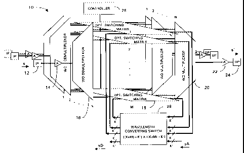
Referring to Fig. 1 there is illustrated a cross-connect switch 10
in accordance with an embodiment of the present invention. The cross-
connect switch 10 includes an input port 12 for receiving an optical signal s,
for example a DWDM optical signal from an optical telecommunications
network. The input port 12 is connected to an optical amplifier 14 via an
optical fiber. Unless stated otherwise, all connections internal to the switch
are
made by way of optical fiber, which may or may not be assembled into ribbon
cables with multiple fibers and associated multi-way connectors. The amplifier
14 amplifies the optical signal s, which might, for example, be received from
a
fiber cable from the previous line amplifier to compensate for the insertion
loss
of the span before it is applied to a wavelength division (WD) demultiplexer
16. The demultiplexer 16 divides the optical signal s into its constituent
channel wavelengths. Each channel has a predetermined wavelength, k1 to
XM assigned to it. In the embodiment of Fig. 1 there are up to 160 such
CA 02285128 1999-11-18
13
channels. A respective optical switching matrix 18 is provided for each set of
channels that have a common predetermined wavelength, one such channel
coming from each of the WD demultiplexers 16. Fig. 1 shows M such optical
switching matrices of which there are up to 160 in the present embodiment
(i.e. M=160), since there are up to 160 channels on each inter-node long haul
transmission fiber. At each channel wavelength, light from the optical signal
s
at the channel wavelength is input into the respective optical switching
matrix
18 for that channel. A wavelength division (WD) multiplexer 20 aggregates a
switched channel from each one of the optical switching matrices into another
io optical signal s' for outputting from an output port 24. Each output port
24 is
connected to the WD multiplexer 20 through an optical amplifier 22. The
optical amplifier 22 amplifies the optical signal s' to compensate for the
insertion loss through the switch 10 before the optical signal s' is output
from
the switch 10 into an optical telecommunications network, for example.
Note that the cross-connect switch 10, in addition to performing optical
switch functions, also restores the level of the optical signals for
transmission
to the next cross-connect switch 10 or destination node. Consequently, the
cross-connect switch, as shown in its entirety in Fig. 1, replaces the entire
WDM/WDD-transponder-cross-connect path that would be required in an
2o electrically switched and regenerated transmission network.
The switch 10 has a plurality of input ports 12 and respective optical
amplifiers 14 and WD demultiplexers 16 as well as a plurality of output ports
24 and respective optical amplifiers 22 and WD multiplexers 20. Fig. 1 shows
N input ports 12, each of which has an accompanying optical amplifier 14 and
WD demultiplexer 16. Fig.1 also shows N output ports 24, each of which
having an accompanying optical amplifier 22 and WD multiplexer 20. In the
present embodiment there are up to 32 input ports and 32 output ports, that is
N=32. However, expansion of the switch 10 to provide a greater number of
input and output ports is possible, and will be described later. Also
possible,
3o are configurations in which the number of input ports does not equal the
number of output ports. For example, rectangular (e.g. 16 x 32) optical
switching matrices 18 could be used to map a reduced subset of transponders
to a provisionable subset of ports within the wavelength group of those
transponders.
CA 02285128 1999-11-18
14
An inter-matrix switch in the form of a wavelength-converting
switch 28 with additional add/drop multiplexer capabilities is connected
across
each of the optical switching matrices 18. That is, for each optical switching
matrix 18, a number (K) of outputs of the wavelength-converting switch 28 are
connected individually to the same number (K) of inter-matrix inputs of that
optical switching matrix 18. As well, for each optical switching matrix 18, a
number (K) of inputs of the wavelength-converting switch 28 are connected
individually to the same number (K) of inter-matrix outputs of that optical
switching matrix 18. In the present embodiment, the number K is a variable
io over the range 0-16, covering the extreme cases of all wavelengths needing
conversion or access to add-drop (K=16) or no wavelengths needing
conversion or access to add-drop (K=0). The preferred value of K is K = 8,
(i.e. 25% of optical switching matrix 18 inputs/outputs, thereby permitting
33%
of the remaining 24 inputs and outputs to be connected to the wavelength
conversion/ add-drop inter-matrix switch.) Other variations are possible. The
wavelength-converting switch 28 also has a capability of converting
wavelengths. That is, it can receive information on one wavelength and
transmit the same information on a different wavelength. This capability is
useful for switching information between channels as described further below.
It should be noted that the wavelength-converting switch 28 can
add/drop channel signals without performing wavelength conversion on the
added/dropped channels signals, hence it can function solely as an add/drop
multiplexer. Conversely, the wavelength-converting switch can perform
wavelength-conversion without performing an add/drop function; hence it can
function solely as a wavelength-converting switch. Moreover, the wavelength-
converting switch 28 can perform both a wavelength conversion function and
an add function on the same channel signal, and separate functions (i.e. add,
drop, convert wavelength) on different signals at the same time, as will be
described later.
The switch 10 also includes a controller 26 for controlling each of the
optical switching matrices 18, the wavelength-converting switch 28 as well as
any tunable transponders or sources associated with the wavelength-
converting switch 28. For example, the controller 26 can set up the optical
switching matrix 18, assigned to channel one, to switch light from the output
of
CA 02285128 1999-11-18
the WD demultiplexer 16, connected to the second input port 12, to the input
of the WD multiplexer 20, connected to the first output port 24. The
controller
26 is connected to each optical switching matrix 18 via electrical cable, and
controls each optical switching matrix 18 using electrical control signals.
The
5 control signals and link over which they are transmitted could also be
optical
in nature, although the control of the crosspoint would likely remain
electrical
in nature. The control signals are generated by a real-time processor (not
shown) of the switch 10 which configures crosspoints of the switch 10 in a
manner similar to that used in an equivalent electrical switch operating under
io Element Manager control from a central Network Manager. Alternatively, the
Element Manager may receive control signals from configuration controllers
distributed among network switching nodes.
An important design consideration of the switch 10 is balancing the
power gain/loss in the "through" path of the switch 10 with that in the
15 "wavelength conversion" path. The "through" path, or link path, is the any
path
through only one optical switching matrix 18, from amplifier 14 to amplifier
22.
In such a path there is no optical regeneration and any losses must be within
the link budget. In the wavelength conversion path, i.e. any path through two
or more optical matrices 18 and the wavelength-converting switch 28, there is
typically optical regeneration performed by transponders in the wavelength-
converting switch 28. It is important that this path, also between the optical
amplifiers 14 and 22 have a power loss/gain in the same range as the through
path. By adjusting the power levels of the transponders in the wavelength-
converting switch 28 the power loss/gain difference between the two types of
paths can be balanced.
In operation the switch 10 is capable of three modes of switching, they
are: port switching, channel switching, and switching that is a combination of
channel and port switching. The operation of the switch 10 in each of these
three modes will be described further by way of example.
In the port switching mode, a optical signal s arrives at input port one
and is split into its constituent channels (1 to 160) by the WD demultiplexer
16
assigned to that port. The controller 26 has set up the optical switching
matrix
18, for channel wavelength one, to switch optical signals from its input from
port number one to its output for port number two. This causes light of
CA 02285128 1999-11-18
16
wavelength Xl from the output of the WD demultiplexer 16 assigned to
channel wavelength one to be directed to the input of the WD multiplexer 20
assigned to the output port two. This light is aggregated with light from the
other channels by the WD multiplexer 20 into the signal s', which is output
from the output port two. Thus, information received by the switch 10 on
channel one input port one is switched to channel one output port two, and is
outputted by the switch 10.
In the channel-switching mode, each channel of the optical signal s
arrives at its respective optical switching matrix 18 from the WD
demultiplexer
io 16 as before. However, in this case the controller 26 has set up the
optical
switching matrix 18 for channel two to switch its input for port one to one of
its
outputs connected to the wavelength-converting switch 28. For example, the
optical switching matrix for channel two has been configured to switch its
input
for port one to the first input of the wavelength-converting switch 28.
Recall,
is that in the present embodiment the wavelength-converting switch 28 has
eight
inputs and eight outputs (K=8) connected to each optical switching matrix 18.
The wavelength-converting switch 28 is also configured by the controller 26
and connected thereto by electrical or optical links (not shown). In this
example, the wavelength-converting switch 28 is configured to receive
20 information on its first input for channel two X2 and output the
information on
channel three X3 at its first output port for channel three. This optical
switching
matrix 18 is set up to direct the light from this signal to its output
connected to
the WD multiplexer 20 for port one. Consequently, information received by the
switch 10 on input port one channel two is output on output port one channel
25 three. Thus, the switch 10 has performed channel switching, from channel
two
input port one to channel three output port one.
In switching that is a combination of port and channel switching,
hereinafter referred to as port-channel switching, information arrives at the
switch 10 on a particular input port number, carried by a particular channel
30 wavelength, and leaves on another output port number, carried by a
different
channel wavelength. The operation of port-channel switching is the almost the
same as channel switching except that in the last switching step the signal is
switched to another output port number. For example, in the previous
CA 02285128 1999-11-18
17
example of channel switching, instead of switching the channel signal back to
output port one (on channel three) it would be switched to any of the other
output ports (e.g. output port four).
The configuration control strategy used to control cross-connect
switches 10 will favour port switching at the cross-connect switches 10 in
preference to channel switching and port-channel switching. Channel
switching and port-channel switching will generally be used only when no
single wavelength channel is available from a source node to a destination
node. The need for channel switching and port switching can be reduced by
io over-provisioning wavelength channels. Such over-provisioning has less cost
impact in an optically switched network than in an electrically switched
network since little of the required equipment is wavelength specific.
A further capability of the switch 10 is the ability to add or drop traffic
using the add/drop multiplexer functionality of the wavelength-converting
1s switch 28. The wavelength-converting switch 28 has K' add inputs for adding
traffic and also K' drop outputs for dropping traffic. In the present
embodiment
K' ranges from 480 to 960, corresponding to a 20% traffic add/drop on a half
to fully configured switch, depending on the number of wavelength channels
that are provisioned on the cross-connect switch 10.
20 In Fig. 1, a signal sA, which is to be added to the traffic flow processed
by the switch, is shown being input to the wavelength-converting switch 28.
This signal sA, could go through wavelength conversion if necessary, as
described above, before being output by the wavelength-converting switch 28
into one of the optical switching matrices 18. The signal sA is then output to
25 one of the WD multiplexers 18 for aggregation into an optical signal, for
example s', to be transmitted from a corresponding output port 24. Also
referring to Fig. 1, a signal sD, which is to be dropped from the traffic flow
processed by the switch, is shown being output from the wavelength-
converting switch 28. This signal sD, could also go through wavelength
30 conversion if necessary, before being output by the wavelength-converting
switch 28 into other optical communications equipment (not shown).
Fig. 2 illustrates, in a functional block diagram, an embodiment of the
wavelength-converting switch 28 shown in Fig. 1. The wavelength-converting
switch 28 includes an electrical switch 30. A plurality of transponder
receiver
CA 02285128 1999-11-18
18
sections for converting line optical signals to electrical signals or short
reach
optical signals, as required by the electrical switch, are connected to the
inputs of the electrical switch 30. Specifically, M groups of K receiver
transponders 32 for converting optical signals from the optical switching
matrices 18 are connected to the electrical switch 30. As well, receiver
transponders 38 for converting optical signals (e.g. the signal sA) to be
"added" to the traffic flow of the transport system via switch 10 are also
connected to inputs of the electrical switch 30. In the present embodiment
K=8 and M=160 and K" = 960, giving a cross-connect size of [(160 x 24) +
io 960] x [(160 x 24) +960] = 4800 x 4800. Such a cross-connect may be
implemented as a single switch or as several (e.g. eight parallel planes of
smaller (600 x 600)) switches, exploiting the lateral interplane cross-
connection inherently available in the optical switch matrices 18 to minimize
any resultant wavelength blocking. In addition, a plurality of transmitter
is transponders for converting electrical signals to optical signals is
connected to
the outputs of the electrical switch 30. That is, M groups of K transmitter
transponders 34 for converting electrical signals for the optical switching
matrices 18 are connected to the outputs of the electrical switch 30. As well,
transmitter transponders 36 for converting electrical signals of dropped
traffic
20 into local cross-office optical signals are also shown connected to outputs
of
the electrical switch 30.
It should be noted, that the transponders 36, 38 are optional and would
be required if optical signals (e.g. the signal sA) are to be added to the
traffic
flow or if dropped signals (e.g. the signal sD) are to be optical. Further, it
25 should be noted that the number of transponders connected to the inputs of
an optical switching matrix 18 does not have to be equal to the number
connected to the outputs of the same optical switching matrix. Still further,
the
receiver transponders 32 need not be very sensitive since they are receiving
light that has been amplified by the optical amplifier 14 and then only
3o attenuated about 5-10 dB by a WD demultiplexer 16 and an optical switching
matrix 18. However, the wavelength-accurate transmitter transponders 34 are
usually expensive, due to their precision optical sources and the number of
versions required (i.e. one for each wavelength in the case of fixed
transponders or one for each wavelength band in the case of tunable
CA 02285128 1999-11-18
19
transponders). Hence, more of the receiver transponders 32 than the
transmitter transponders 34 may be provisioned to optimize the wavelength
conversion capability at the lowest cost.
Operation of the wavelength-converting switch 28 will now be
explained by way of example. The receiver transponder 32 receives an optical
signal Sc1, on channel one (i.e. channel wavelength k1) from a optical
switching matrix 18 assigned to channel one and converts the information in
this signal to an electrical signal Ec1, which is input to the electrical
switch 30.
The electrical switch 30 has a switching granularity of the entire signal
lo payload of each wavelength channel. The electrical switch 30 switches the
electrical signal Ec1 to one of its outputs assigned to channel fifty. The
transmitter transponder 34 receives the signal Ec1 and converts the
information carried by it to an optical signal Sc50 having a wavelength
corresponding to channel fifty. This signal is output to the optical switching
matrix 18 that is assigned to channel fifty, which directs it to a WD
multiplexer
20, as described earlier. Thus, since the information in the optical signal
Sc1
has been switched to the optical signal Sc50, a channel switching function, or
wavelength conversion function (i.e. from channel wavelength M to channel
wavelength X50) has been performed by the wavelength-converting switch 28.
In a similar manner the signal sA is directed into the electrical switch 30
via
the receiver transponder 38 and is forwarded into the one of the optical
switching matrices 18 via one of the transmitter transponders 34. Likewise,
the signal sD is directed out of the switch 10 via the receiver transponder 32
and into the electrical switch 30, where it is forwarded into other
communications equipment via the transmitter transponder 36.
Fig. 3 illustrates, in a functional block diagram, an embodiment of the
receiver transponders 32, 38 of Fig. 2, both of which are identical in
structure.
However, this need not be the case. The add-drop transponders 36, 38 may
not need to be as high precision devices (i.e. high sensitivity receiver,
precise
wavelength transmitter) as the transponders linked to the switch matrices 18
unless they are going into another line system directly. If they are feeding a
Terabit router they may well be short reach optics, for example, 1310 nm or
850 nm ribbon optics. The receiver transponder 32 includes a long range
CA 02285128 1999-11-18
receiver 32a connected to its input for receiving an optical signal. The long
range receiver 32a has enough sensitivity to receive and detect data on
optical signals that are at the minimum specified power level and signal-noise
ratio of the optical communications network in which the switch 10 is used. A
5 local interface 32b is connected at the output of the receiver transponder
32
and is in communication with the long-range receiver 32a. The local interface
32b receives data from the long-range receiver 32a that it has detected and
outputs this information in an electrical signal.
Fig. 4 illustrates, in a functional block diagram, an embodiment
io of the transmitter transponders 34, 36 of Fig. 2, both of which are
identical in
structure. The transmitter transponder 34 includes a local interface 34a,
connected to its input, for receiving an electrical signal and detecting data
contained therein. A long reach transmitter 34b of high precision is connected
at the output of the transmitter transponder 34 and is in communication with
15 the local interface 34a. The long reach transmitter 34b receives the
detected
data from the local interface 34a and outputs this information in an optical
signal.
Fig. 5 illustrates, in a pictorial diagram, an embodiment of the
switching matrix 18 of Fig. 1. The switching matrix 18 has N inputs and N
20 outputs. A subset K of the inputs are intra-node inputs and are for
receiving
added or converted signals from the wavelength converting switch 28, which
provides both add/drop and wavelength conversion capabilities as discussed
previously. The remaining inputs, N-K in number, are inter-node inputs for
receiving channel signals from other nodes. Similarly, a subset K of the
outputs are intra-node outputs and are for transmitting signals to the
wavelength-converting switch 28 that are to be dropped or wavelength
converted. The remaining outputs, N-K in number, are inter-node outputs for
outputting channel signal destined for other nodes.
A switching element 19 is shown in the form of a Micro-Electro-
Mechanical System (MEMS)-based switching element. The MEMs-based
switching element 19 comprises optical diverters 48, 50 arranged in rows and
columns to direct light from an input on the perimeter of the arrangement of
optical diverters to an output also on the perimeter of the arrangement. The
MEMS-based switching element 19 has row outputs, which are in alignment
with the inputs and are on the opposite side of the arrangement of optical
diverters 48, 50 relative to the inputs. The MEMS-based switching element 19
CA 02285128 1999-11-18
21
also has column outputs situated along paths at right angles with paths
between the inputs and row outputs. A self-focusing collimating lens 52 at
each input of the MEMS-based switching element 19 directs light received
from an optical fiber 54 into the arrangement of optical diverters. At each
row
and column output another self-collimating lens 56 and 56', respectively,
receives light from the arrangement and directs the light along a respective
fiber 58 and 58'. The controller 26 controls the state of each of the optical
diverters, through a mirror drive signal, in order to direct the light as
required.
Fig. 5 shows an optical diverter 48, or mirror, in an activated state,
whereby,
io an optical signal Sc1 entering the arrangement of optical diverters along a
row
is redirected along a column to the self-collimating lens 56' at the
respective
column output of the MEMS-based switching element 19. The other optical
diverters in the figure are shown in a non-activated state, for example,
optical
diverter 50, whereby an optical signal Sc2 is not redirected. The optical
signal
Sc2 passes through the arrangement and enters the collimating lens 56
where it is passed along the fiber 58. The switching matrix 18 is a self-
contained switch circuit pack, providing all the switching interconnect needs
of
all the ports and all the inter-matrix feeds for one wavelength. It achieves
this
by incorporating, as part of its functionality, an optical crosspoint array
(i.e.
using one or more MEMS-based switching elements). One or more complete
switching matrix can be accommodated on a physical circuit pack.
Fig. 6 illustrates, in a functional block diagram, the MEMS-based
switching element 19. The MEMS-based switching element 19 is a 32 x 32
array. A MEM switching device is disclosed in an OFC99 paper entitled "Free-
space Micromachined Optical-Switching Technologies and Architectures",
by Lih Y. Lin of AT&T Labs-Research, and published in OFC99 Session
W14-1, Feb. 24, 1999 proceedings. MEMS switching devices are
commercially available components manufactured using silicon
microelectronic processing. MEMS switching devices can be "square" (i.e. the
number of inputs equals the number of outputs), resulting in an n x n array
where "n" conventionally equals 8, 16, 32, etc. MEMs switching devices can
also be "rectangular" (i.e. the number of inputs is not equal to the number of
outputs), resulting in an n x m array where n and m are conventionally 8, 16,
32, etc. The optical diverters 48, 50 of Fig. 5 are optically reflective
elements,
for example mirrors. An optical diverter in an activated state (e.g. the
optical
CA 02285128 2007-05-28
22
diverter 48 in Fig. 5) typically inserts a 3-7 dB loss in optical power in the
redirected signal (e.g. the signal Sc1 in Fig. 5), depending upon the MEMS
switching device port count, the quality of the design and the fabrication of
the
parts. A signal that passes through a MEM switching device into one of its row
outputs (e.g. the signal Sc2 in Fig. 5) usually has a lower drop in power,
typically 1-2 dB, again dependent upon device size and design. Although
MEMS switching devices are shown in this embodiment of the active
crosspoints of the switching matrix 18, any matrix of optical diverters
capable
of directing light of the required wavelength, and as desired, could be used.
Fig. 7a illustrates, in a functional block diagram, a second embodiment
of the switching element 19, shown for the first channel wavelength %l . The
switching element 19 of the 32 x 32 optical switching matrix 18 are comprised
of four 16 x 16 MEM devices 19a1, 19a2, 19b1, and 19b2, which are
controlfed by the controller 26. The MEM device 19a1 has sixteen inputs ip1
to ip16, which are connected to the WD demultiplexers 16 of the ports one to
sixteen, respectively. The MEM device 19a1 has two sets of outputs, one set
of column outputs corresponding to the resultant path of an optical signal
that
has been directed by an optical diverter in an activated state. The column
outputs are labeled op1 to op16 in the figure. The other set of outputs are
row
outputs corresponding to the path of an optical signal which is not directed
by
any optical diverters. That is, all of the optical diverters in the path of
the
optical signal are in a non-activated state (e.g. the optical diverter 50
shown
in Fig. 5). The row outputs of the MEM device 19a1 are connected to the
inputs of the MEM device 19a2. The column outputs of the MEM device 19a2
are labeled op17 to op32. Likewise, the MEM devices 19b1 and 19b2 are
connected in a similar manner for inputs ip17 to ip32 and outputs op1' to
op32'. Each of the column outputs op1 to op32 from the MEM devices 19a1
and 19a2 are combined with its respective row output op1' to op32' from the
MEM devices 19b1 and 19b2. This is done using thirty-two 2:1 combiners,
one of such combiners 70 is shown for port thirty-two. These combiners are
single mode compatible combiners. Both fused fiber couplers and Silica on
Silicon waveguide structures are appropriate. Both of these technologies will
add about 3 -3.5 db of loss to the cross-switch budget. The combiner 70
CA 02285128 2007-05-28
23
combines the outputs op32 and op32' to produce an output op32". An optical
signal will appear at the output op32 or op32', depending on which input an
optical signal destined for port thirty-two is applied. For example, an
optical
signal applied to the input ip1 will be output at one of the outputs op1 to
op32,
whereas an optical signal applied to the input ip17 will be output at one of
the
outputs op1' to op32'. The output of each 2:1 combiner is connected to the
WD multiplexer 20 of its respective output port, at the input for the first
channel wavelength X1, and the resultant multiplexed signal is forwarded to
the optical amplifier 22 for that port. Using this arrangement an optical
io switching element 19 of a given dimension can be implemented using MEMs
of smaller dimension. In this case, the switching element 19 is realized using
two pairs of smaller switching elements 19a1, 19a2 and 19b1, 19b2.
Fig. 7b to 7d illustrate, in functional block diagrams, other embodiments
of the optical switching element 19, shown for the first channel wavelength M.
Several variations exist on the theme of using the through port / third port
of a
MEMS device. One of these, already described with reference to Fig. 7a, is to
make 32 x 32 switches out of 16 x 16 switches. Such an approach is useful
before 32 x 32 MEMs devices are readily commercially available. Another
variation, shown in Fig. 7b, is to use four 32 x 32 MEMS modules to build a 64
x 64 switching element 19 for each channel wavelength. The result is an
approximately 10000 x 10000 wavelength switch capacity, assuming 160
channel wavelengths. Still another variation, shown in Fig. 7c, is to
partition
the cross-connect switch 10 such that the initial implementation is 32 x 32 on
an initial optical switching matrix card 72, but an expansion port 73 is
provided. This expansion port 73 and an extension board 74 is used to extend
the initial optical switching matrix card 72 of the switch 10 to the size of
32 x
64. In this case an identical switch having another 32 x 64 optical switching
card 75, can then be used to create a switch having double the capacity in
terms of port count. In this case two alternatives exist for coupling together
the
outputs. The first is shown in Fig. 7c, where per port per wavelength
combiners 70 are provided, of which there would be sixty-four per wavelength,
and therefore 64 x 160 per switch. The output of each combiner would be
connected to a respective channel wavelength input of a wavelength division
CA 02285128 1999-11-18
24
multiplexer 20 assigned to the respective port. The other approach, shown in
Fig. 7d, is to reverse the sequence combining outputs of the MEMs and
multiplexing of the combiner outputs. In this approach two banks of
wavelength division multiplexers 20a, 20b multiplex the outputs of the MEMs,
one multiplexer per port multiplexing M channel signals. That is, the first
bank
of multiplexers 20a, multiplexes the outputs op1 to op64 using one multiplexer
per port, each multiplexer multiplexing M channel signals of distinct
wavelength, and the second bank of multiplexers 20b, performing the same
function for ports opl'to op64'. The resultant multiplexed signals of the
banks
io 20a, 20b are combined on a port-by-port basis by respective combiners 70.
Two such resultant multiplexed signals 77a and 77b are in the figure. The
output of each combiner 70 is then applied to a respective optical amplier 22
for the port. This approach increases the number of output WDM multiplexers
20a, 20b from 64 to 128, but reduces the number of combiners 70 from 64 x
160 down to 64. The approach also greatly simplifies cabling. Both of the
variations shown in Figs. 7c and 7d allow the optical telecommunications
switch to expand in the ports per wavelength direction.
Fig. 8 illustrates, in a functional block diagram, a second
embodiment of the wavelength-converting switch 28. The wavelength-
converting switch 28 includes K channel convertors 80. Each channel
convertor 80 has M inputs and M outputs. There is one input and one output
for each channel wavelength. Each optical switching matrix 18 for a particular
channel wavelength has an inter-matrix output connected to the input for the
corresponding channel wavelength and an intermatrix input connected to the
output for the corresponding channel wavelength of each channel convertor
80.
As noted above with reference to Fig. 1, typically 25% of the
inputs and outputs of the optical switching matrix 18 are connected to the
wavelength-converting switch 28. Thus, a channel convertor is required for
3o each of these input/output connections. Accordingly, K=8 in the case of the
optical switching matrices 18 being 32 x 32 matrices. Furthermore, as shown
in Fig. 1, there are K' inputs/outputs on the wavelength-converting switch 28
for add/drop traffic.
CA 02285128 1999-11-18
As shown in figure 8, the K' drop outputs and the K' add inputs
are distributed equally among the K cards, resulting in K'/K drop outputs and
K'/K add inputs per card. Each channel convertor 80 has an MxM optical
switch 82 connected to the inputs of the wavelength-converting switch 28.
5 Since there are K channel convertors 80, the number of inputs that the
wavelength-converting switch 28 has is KxM, which equals 1280 inputs. The
wavelength-converting switch 28 also has 1280 outputs. A subset L of the
outputs of the MxM optical switch 82 are each connected to respective optical
receivers 84. In this embodiment the number L equals 32, but could be any
io number less than or equal to M. The MxM optical switch 82 directs input
optical signals to the optical receivers 84 according to its connection map,
which is determined by the controller 26. Each optical receiver 84 converts a
received input optical signal into an electrical signal and outputs the
electrical
signal to a selector 90. The selector 90 provides includes the K'/K inputs for
15 adding channel signals and the K'/K outputs for dropping channel signals.
The
controller 26 controls the operation of adding and dropping channel signals
via the selector 90. This operation is shown as being done with electrical
signals however the selector 90 could include opto-electric conversion
capabilities to add/drop optical channel signals. The selector 90 forwards
2o electrical signals to a tunable optical source 86. There are L tunable
optical
sources 86. Each tunable optical source 86 is operable over a range of M
channel wavelengths. Currently available tunable sources typically have a
tunable range of thirty-two channel wavelengths, however this range is
increasing. Each tunable optical source 86 receives an electrical signal from
25 the optical receiver 84 to which it is connected and outputs an output
optical
signal, which contains information present in the input optical signal, to
another MxM optical switch 88. The output optical signal has a channel
wavelength equal to the wavelength at which the controller 26 has set the
tunable source 86. The MxM optical switch 88 directs output optical signals,
3o according to its connection map set by the controller 26, to the outputs of
the
channel convertor 80.
The operation of the channel convertor 80 will now be further
explained by way of example. An optical signal Sc1, of channel one
CA 02285128 1999-11-18
26
wavelength X1, is applied to the first channel convertor 80 at the first input
of
the MxM optical switch 82. The optical signal Sc1 is directed by the MxM
optical switch 82 to the first optical receiver 84. The first optical receiver
84
converts the information contained in the optical signal Sc1 into an
electrical
signal Ec1. The electrical signal Ec1 passes through the selector 90 and is
applied to the first tunable source 86. The first tunable source 86 has been
set
to output an optical signal at the channel twenty wavelength k20. The first
tunable source 86 outputs an optical signal Sc20, which contains the
information in the electrical signal Ec1, to the first input of the MxM
optical
io switch 88. The MxM optical switch 88 directs the optical signal Sc20 to the
twentieth output of the channel convertor 80. The optical signal Sc20 is then
further directed by the optical switching matrix 18 assigned to channel
twenty.
Fig. 9 illustrates, in a functional block diagram, a third
embodiment of the wavelength converting switch shown in Fig. 1. This
embodiment includes K/S, S*M x S*M channel convertors 92, where
M=160 and S= 2 in Fig. 9. Selection of a value for S will be explained
later. The structure of the channel convertor 92 will be explained with
reference to Figs. 11 to 13 which provide tables specifying
interconnections between components of the channel convertor 92. The
channel convertor 92 has S*M inputs and S*M outputs. The inputs and
outputs are arranged in S banks, in this case there are two banks, bank1
and bank2. Each bank has an input and an output for each of the channel
wavelengths. That is, there are M inputs and M outputs per bank. The
inputs/outputs of the banks connect to inter-matrix outputs/inputs of the
appropriate switching matrices according to their channel wavelength. In
the present embodiment of the switch 10, where K=8, the wavelength-
converting switch includes four 2M x 2M channel convertors 92.
The channel convertor 92 includes an optical switch100
(OXCA), which comprises five 32 x 32 optical switches OXC1 to OXC5.
3o The optical switch 100 is connected to the first bank of inputs via an
interconnect 102 (interconnect A). The interconnect 102 connects the
inputs of bankl, MA160, to the inputs of the optical switch 100
according to table 1 in Fig. 11. For example, table 1 shows that the input
M is connected to the input 11 of the 32 x 32 optical switch OXC1. The
remaining inputs of the optical switch OXC1 are connected to every fifth
input of bankl (e.g. 12 connected to X6, 13 to M 1, and so on). Similarly,
CA 02285128 1999-11-18
27
the optical switches OXC2 to OXC5 have inputs connected every fifth
input of bank1 starting at input X2 to k5, respectively, as shown in table1 .
The channel convertor 92 also includes another optical switch 104
(OXCB) and another interconnect (interconnect B) connected in a similar
manner to the inputs of bank2, as shown in table2 of Fig. 11.
The channel convertor 92 further includes a wavelength
convertor 108 which is connected to the optical switches 100, 104
(OXC_A and OXC_B) via an interconnect 110 (interconnect C). The
wavelength convertor 108 includes ten convertor modules 106, labelled
io G1 to G10. Each convertor module 106 includes up to 32 tunable
transponders, a 32 x 32 optical switch, 32 inputs labelled 1(1:32) and 32
outputs labelled 0(1:32). The convertor module 106 will be described in
more detail later. The value of S, referred to earlier, is chosen to match
the range of the tunable transponders to the size of the optical switches
in the convertor modules G 1 to G 10. In this case, the transponders have
a range of 16 channel wavelengths and the optical switches are 32 x 32,
hence S is 32/16 = 2. The interconnect 110 connects the inputs of the
wavelength convertor 108 to the outputs of the two optical switches
100, 104, as shown in table 3. For example, the first ten outputs of the
optical switch OXC1 (01 to 010) are connected to the first input of the
convertor modules G1 to G10, respectively. Likewise, the second and
third sets of ten outputs (011- 020 and 021- 030) of the optical switch
OXC1 are connected to the second and third inputs of the convertor
modules G 1-G 10, respectively. The remaining two outputs 031 and 032
of the optical switch OXC1 are connected to the thirty-first inputs of the
first and second convertor modules G1 and G2, according to table 3. The
remaining optical switches OXC2 to OXC5 of the optical switch 100
(OXC_A) are connected in a similar manner as shown in table3 of Fig. 12.
Similarly, the outputs of the optical switch 104 (OXC B) are connected to
the wavelength convertor in a similar manner, as shown in table3.
The outputs of the wavelength convertor 108 are connected
to the two banks of outputs via another interconnect 1 12
(interconnect_D), as shown in table4 of Fig. 13. For example, the first
sixteen outputs 01-016 of the convertor module G1 are connected to the
first sixteen outputs M-M6of bankl, respectively. The remaining sixteen
outputs 017-032 are connected to the first sixteen outputs MA16 of
bank2, respectively. The remaining convertor modules G2 to G10 are
CA 02285128 1999-11-18
28
connected in a similar manner to the remaining outputs in the banks,
according to table4.
The wavelength convertor 108 also has add inputs and drop
outputs for adding/dropping channel signals. Since the wavelength
converting switch 28 provides K' of each such inputs/outputs then each
2M x 2M channel convertor, and hence each wavelength convertor 108,
provides 2K'/K add inputs and 2K'/K drop outputs. This will be explained
in more detail later.
The controller 26 controls the operation of the optical
to switches 100, 104 (OXC_A and OXC_B) and the wavelength convertor
108.
The interconnects 102, 106, 112 (interconnect A,
interconnect_B and Interconnect_D) would typically be implemented as
optical fiber connection. However, the interconnect 110 (interconnect D)
could be optical fiber, but could additionally include several 32 x 32
optical switches which interact with the optical switches 100,104 and
the optical switches in the convertor modules G 1 to G 10 to create a
standard CLOS arrangement.
Operation of the third embodiment of the wavelength-
converting switch 28 will now be further explained by way of example. A
channel signal Sc1 of a first wavelength k1 arrives at the first input M of
bank1 . The interconnect 102 (interconnect_A) connects the signal Sc1 to
the first input 11 of the optical switch OXC1 which routes the signal Sc1
to its tenth output 010. The interconnect 110 (interconnect C) connects
the signal Sc1 to the first input 11 of the tenth convertor module G10.
The tenth convertor module G 10 receives the signal Sc1, converts it to
another channel signal Sc160 of the 160 channel wavelength M 60, and
routes the signal Sc160 to its sixteenth output 016. The interconnect
1 12 (interconnect_D) connects the signal Sc160 to the 160th output
a,160 of bank1 where it is output from the wavelength-converting switch
28, into one of the ports on the optical switching matrix 18 associated
with the channel wavelength X160.
Fig. 10 illustrates in a functional block diagram an embodiment
of a converter module 106 shown in Fig. 9. The convertor module 106
includes receivers 114, connected to the inputs 11 to 132, a selector 115
connected to the outputs of the receivers 114 for add/drop capability, and
tunable transponders 116, connected to the outputs of the selector 115.
The tunable transponders 1 16 are tunable over a range of sixteen channel
CA 02285128 1999-11-18
29
wavelengths in this embodiment. The convertor module 106 is
provisionable for up to 32 tunable transponders however, options exist
where some of the tunable transponders can be replaced by fixed
transponders. Each receiver 114 can receive a channel signal of any of
the M wavelengths, and convert the received channel signal to an
electrical signal. The selector 1 15 is used to add/drop electrical signals
in/out of the convertor module. There are Q add inputs and Q drop
outputs shown in Fig. 10, where Q= 2K'/10K. The value for Q is derived
from the total number (K') of add/drop inputs/outputs for the wavelength
to converting switch 28 divided by the number of S*M x S*M channel
convertors (K/2) divided by the number of wavelength convertor modules
(10). The outputs of the transponders 116, are connected to the inputs of
a 32 x 32 optical switch 118. The optical switch 118 routes each
channel signal it receives to an output according to the wavelength of the
channel signal being routed. Operation of the tunable transponders 1 16
and the optical switch 1 18 is under control of the controller 26.
Numerous modifications, variations, and adaptations may be made to
the particular embodiments of the invention described above without
2o departing from the scope of the invention, which is defined in the claims.
For
example, the electrical inter-matrix switch 30 in Fig. 2 could be replaced
with
an optical switch which can be made out of a multi-stage array of MEMS
devices since the cross-connect is sitting between transponder banks and is
not part of the line system optical reach budget where loss is critical.
The optical loss of a 32 x32 MEMS is likely to be about 6-8 dB, so the
insertion loss of one pass through a switching matrix 18 does not approach
the inter-amplifier link budget (approximately 24 dB).
The plurality of receiver transponders 32 could convert optical signals
to short reach optical signals if the output signals of the cross-connect
switch
10 are only required to be routed to terminal equipment at the same node.