Note: Descriptions are shown in the official language in which they were submitted.
CA 02286531 1999-10-18
- 1 -
PATENT
ATTORNEY DOCKET NO: 07289/O11CA1
FEEDFORWARD AMPLIFICATION SYSTEM HAVING MASK DETECTION
COMPENSATION
Background of the Invention
This invention relates generally to amplification
systems and more particularly to methods and apparatus
for reducing distortion in amplifiers used in such
systems.
As is known in the art, amplifiers have a wide
variety of applications. Amplifiers can be biased to
operate in one of a number of so-called Classes. When
biased to operate in Class A, the amplifier provides a
linear relationship between input voltage and output
voltage. While operation in Class A has a wide range of
applications, when higher power output and efficiency are
required or desired, the amplifier is sometimes biased to
operate in Class A/B. When biased to operate in Class
A/B, however, the Class A/B amplifier power transfer
curve 10 is less linear than for Class A amplifiers,
illustrated in FIG. 1 by trace 14. To increase
efficiency, communication systems often operate
amplifiers in the non-linear region 12. This practice,
however, does introduce amplitude and phase distortion
components into the output signal produced by the
amplifier.
As is also known in the art, most communication
systems have FCC allocated frequency bandwidths 18 (that
is, in-band frequencies) centered about a carrier
frequency 20 as shown in FIG. 2A. For example, a CDMA
(Code Division Multiple Access) communication system
signal has a predefined bandwidth of 1.25 MHz. Different
CDMA communication channels are allocated different bands
of the frequency spectrum. Amplifiers are used in such
systems, and are frequently biased to operate in Class
A/B. Referring to FIG. 2B, signal processing such as
CA 02286531 1999-10-18
- 2 -
amplification by an amplifier operating in the non-linear
region 12 (FIG. 1) can produce distortion frequency
"shoulders" 22a-22b outside a signal's allocated
bandwidth 18. (These are called out-of-band
frequencies.) These distortion frequency components 22a-
22b can interfere with bandwidths allocated to other
communication signals. Thus, the FCC imposes strict
limitations on out-of-band frequency components.
Many techniques exist to reduce out-of-band
distortion. One such technique is shown in FIG. 3 where
a predistortion unit 24 is fed by a signal 25 to be
amplified. The predistortion unit 24 has a power
transfer characteristic 24a (Fig. 1) and compensates for
distortion introduced by subsequent amplification in
Class A/B amplifier 26. More particularly, the
predistortion unit 24 transforms electrical
characteristics (for example, gain and phase) of the
input signal such that subsequent amplification provides
linear amplification to the phase and frequency
characteristics of the input signal. The predistortion
unit 24 is configured with a priori measurements of the
non-linear characteristics of the Class A/B amplifier.
Unfortunately, the amplifier characteristics
(amplification curve 10 with region 12 of FIG. 1) change
over time and temperature making effective predistortion
more difficult. For example, as the temperature of the
amplifier increases, its non-linear region 12 may become
more or less linear, requiring a compensating change in
the transform performed by a predistortion unit 24. Some
adaptive predistortion systems use look-up tables to
alter predistorter characteristics based on environmental
factors such as temperature. These look-up tables
include predetermined predistorter control settings for
use in predetermined situations. However, environmental
factors alone do not determine the alterations in an
CA 02286531 2006-01-17
69675-537
- 3 -
amplifier's characteristics. Thus, over time, amplifier
characteristics vary unpredictably due to aging of
amplifier components.
Another approach to reduce amplifier distortion is
to use feedforward compensation, as shown in FIG. 4.
Here, a feedforward network 31 is included for~reducing
out-of-band distortion. The feedforward network 31
includes a differencing network or combiner 30, a main
amplifier 33 operating as a Class A/B amplifier,,an error
amplifier 32, delay circuits 28 and 28a, and a combiner
29. The differencing network 30 produces an output
signal representative of the difference between a portion
of the signal fed to the amplifier 33 operated Class A/B
and the signal fed to the amplifier 33 prior to such
amplification. The frequency components in the
differencing network 30 output signal are, therefore, the
out-of-band frequency components 22a-22b introduced by
amplifier 33. Amplifying and inverting the output
produced by the differencing network 30, by error
amplifier 32, produces an out-of-band correcting signal.
More particularly, the combiner 29 combines the
correcting signal produced by differencing network 30 and
amplifier 32, with the delayed signal output of amplifier
33 thus reducing the energy in the out-of-band
frequencies 22a-22b (FIG. 2B) of the signal output by
amplifier 33. Feedforward network 31 includes delay line
28 to compensate for the delay in error amplifier 32. It
should be noted that minute differences in timing between
these elements can impair the effectiveness of a
feedforward system. While a manufacturer can carefully
match components prior to shipment, as feedforward
components age, the correcting signal and processed
signal can become mistimed if not properly compensated.
id
CA 02286531 2006-01-17
69675-537
- 4 -
Summary of the Invention
According to one aspect of the present invention,
there is provided apparatus for reducing out-of-band
frequency components of an amplified RF input signal derived
from an input signal, the input signal having in-band
frequency components and the amplified RF signal having both
in-band frequency components and out-of-band frequency
components, such apparatus receiving a delayed input signal
having in-band frequency components, such apparatus
comprising: (A) a feedforward network, comprising: (i) a
first combiner coupled to the delayed input signal and the
amplified RF signal; (ii) a variable gain-phase network
controlled by first and second control signals and connected
to the output of the combiner, and (iii) an error amplifier
connected to the variable gain-phase network, such error
amplifier having an output connected to a second combiner;
wherein the control signals operate to reduce the out-of-
band frequency components of the amplified RF signal when
the output of the error amplifier is coupled to a delayed
version of the amplified RF signal; and (B) a feedback loop
comprising a control system having a controller responsive
to a combined output of said error amplifier and said
amplified RF signal, and said control system receiving the
out-of-band frequency component signal and homodyning the
signal to baseband by combination with at least a portion of
said input signal, the control system including filtering
and analysis circuitry arranged to detect energy in the out-
of-band frequency components of such signal for producing
control signals by measuring the energy of the homodyned
signal at at least one selected bandpass frequency, being
coupled to the gain-phase network from the feedback loop for
adjusting the characteristics of the gain-phase network in
CA 02286531 2007-02-14
69675-537
- 4a -
accordance with out-of-band frequency components in said
amplified RF signal.
In a particular aspect of the invention, the
feedback loop has a microprocessor, a frequency generator
responsive to the microprocessor, a mixer having a first
input coupled to the second combiner output and a second
input coupled to the frequency generator. The feedback loop
further has filtering and analysis circuitry including a
bandpass filter and an analog-to-digital converter for
measuring the energy which is out-of-band at at least one
selected bandpass frequency and wherein the microprocessor
in response to the filtering and analysis circuitry, sweeps
the frequency generator output across a band of selected
frequencies to find a carrier frequency of the input signal.
Thereafter, the
CA 02286531 1999-10-18
- 5 -
microprocessor reduces the energy in the out-of-band
frequency components of the amplified signal to a
selected minimum.
In specific aspects of the invention, the input
signal is a CDMA signal and the feedback loop locates the
input signal's allocated bandwidth.
Accordingly, the invention advantageously
provides, in a feedforward RF high power amplifier, a
method of using the out-of-band energy in the Class A/B
amplified signal to reduce distortion and improve the
distortion compensation. The error amplifier signal can
be mixed or homodyned to baseband to enable better
resolution of the detected signal by a "standard"
distortion and analysis circuitry.
Brief Description of the Drawings
Reference is made to the following drawings, in
which:
FIG. 1 is a graph illustrating amplifier output
regions according to the PRIOR ART;
FIGS. 2A and 2B are diagrammatical sketches of a
signal having in-band and out-of-band frequency
components according to the PRIOR ART;
FIG. 3 is a diagrammatical sketch of an
amplification system according to the PRIOR ART;
FIG. 4 is a diagrammatical sketch of another
amplification system according to the PRIOR ART;
FIG. 5 is a diagrammatical sketch of an
amplification system having a predistorter with
adjustable electrical characteristics according to the
invention;
FIGS. 6A-6C are diagrammatical sketches of
frequency spectra of signals produced in the
amplification system of FIG. 5;
CA 02286531 1999-10-18
- 6 -
FIG. 7 is a diagrammatical sketch of the
amplification system of FIG. 5, a control system of such
amplification system being shown in more detail;
FIG. 8 is a flow chart of the process used by the
control system in FIG. 7 to produce control signals based
on energy in out-of-band frequency components;
FIG. 9 is a flow chart of the process used by the
control system of FIG. 7 to determine frequency
components of a signal produced in the amplification
system of FIG. 7;
FIG. 10 is a diagrammatical sketch of an
amplification system having a predistorter with
adjustable electrical characteristics according to
another embodiment of the invention;
FIG. 11 is a diagrammatical sketch of a mixer
configured as a four quadrant multiplier biased into a
linear operating region, such mixer being adapted for use
in the amplification system of FIG. 10;
FIG. 12 is a diagrammatical sketch of the
amplification system of FIG. 10, a control system of such
amplification system being shown in more detail;
FIG. 13 is a diagrammatical sketch of an
amplification system according to another embodiment of
the invention, such amplification system having a
cancellation network configured to increase dynamic range
of out-of-band signal components;
FIG. 14 is a diagrammatical sketch of an
amplification system, such amplification system having a
cancellation network configured to increase dynamic range
of out-of-band signal components according to another
embodiment of the invention;
FIG. 15 is a diagrammatical sketch of an
amplification system, such amplification system having a
cancellation network configured to increase dynamic range
CA 02286531 1999-10-18
- 7 -
of out-of-band signal components according to another
embodiment of the invention;
FIG. 16 is a diagrammatical sketch of an
amplification system having adjustable characteristics
being controlled by the control system of FIG. 5
according to the invention;
FIG. 17 is a diagrammatical sketch of an amplifier
having adjustable characteristics being controlled by the
control system of FIG. 10 according to the invention;
FIG. 18 is a diagrammatical sketch an
amplification system having a feedforward network with
adjustable electrical characteristics controlled by the
control system of FIG. 5 according to the invention;
FIG. 19 is a diagrammatical sketch of an
amplification system having a feedforward network having
adjustable characteristics being controlled by the
control system of FIG. 10 according to the invention;
FIG. 20 is a diagrammatical sketch of an
amplification system having a control system adapted to
control the adjustable electrical characteristics of the
feedforward network of FIG. 18;
FIG. 21 is a diagrammatical sketch of an
amplification system having a control system controlling
multiple components according to the invention.
Description of the Preferred Embodiments
Referring to FIG. 5, an amplification system 100
is shown amplifying an input signal fed thereto on a line
101. More particularly, the system 100 provides an
amplified output signal on a line 103. The system 100
includes an amplifier 102, a control system 104, the
details being shown in FIG. 7), and a predistorter 105,
all arranged as shown. The input signal on line 101, in
this embodiment, is a received CDMA signal. The received
signal has a pre-determined, a priori known, bandwidth
"BW"; however, the carrier frequency fc of such received
CA 02286531 1999-10-18
- 8 -
signal may be any one of a plurality of available carrier
frequencies and is not known in advance.
The amplifier 102 is biased to Class A/B, and thus
has a non-linear amplification characteristic.
Therefore, non-linear amplification by the amplifier 102
will introduce amplitude and phase distortion into the
amplified output signal. Thus, passing a signal through
the amplifier 102, operating with a non-linear output
power versus input power transfer characteristic produces
frequency components outside the bandwidth BW (that is,
out-of-band frequency components).
In this illustrated embodiment, however, the
output signal produced by the amplifier 102 is fed, using
the control system 104, to the predistorter 105. The
predistorter 105 has adjustable electrical
characteristics, for example, adjustable bias
characteristics and parameters. The predistorter 105
receives the input signal on line 101 and the output of
the control system 104, over line(s) 109. The output of
the predistorter 105 is fed to the amplifier 102. The
predistorter 105 has a non-linear gain versus input
signal level characteristic selected in accordance with
an out-of-band feedback control signal (the signals over
line(s) 109) to enable the amplification system 100 to
provide a substantially linear amplifier output power
versus input signal power transfer characteristic to the
input signal 101. Thus, in the steady-state, the output
on line 103 is an amplification of the input signal on
line 101 without, or with reduced, out-of-band frequency
components. As will be described, any out-of-band
frequency energy in the output signal on line 103, as the
result of drift in the amplifier 102, for example, is
detected and is fed to the predistorter 105 using the
control system 104 to enable the system 100 to again
CA 02286531 1999-10-18
- 9 -
produce, in the steady-state, an output signal on line
103 with little, or no, out-of-band frequency components.
More particularly, a feedback loop 107 is provided
wherein the control system 104 receives the output of the
amplifier 102 and produces the feedback control signal on
line 109 for the predistorter 105. The control system
104 analyzes the signal produced by the amplifier 102 to
locate a carrier frequency having the bandwidth BW of the
received signal, here the carrier frequency of the input
signal on line 101, and to produce the feedback control
signal on line 109 related to the energy in the
distortion frequency components (that is, the energy out
of the bandwidth BW) detected in the output signal on
line 103. In the illustrated embodiment, the control
system 104 measures the energy of the distortion
frequency components by measuring energy at a frequency
or frequencies offset from the carrier frequency (for
example, at frequencies 800 KHz and 1.25 MHz from the
carrier frequency), the measurement frequency(s) being
outside of the bandwidth of the input signal. The
feedback control signal on line 109 is coupled to the
predistorter 105 for adjusting characteristics of the
predistorter 105 (for example gain and phase, or
predistorter bias points) and thereby null (that is,
reduce) the energy in the out-of-band signals on line
103.
Referring again to FIG. 5, in one embodiment, the
control system 104 heterodynes to baseband the amplified
signal on line 103 with the carrier frequency of the
received signal and measures the energy in the output
signal on line 103 at one or more predetermined offsets
from the carrier frequency. Referring also to FIGS. 6A-
6C, the frequency spectrum 18 of the input signal on line
101 is shown in FIG. 6A. The frequency spectrum of the
output signal on line 103, in a non-steady-state
CA 02286531 1999-10-18
- 10 -
condition, that is before correction, is shown in FIG. 6B
to have out-of-band frequency components 22a, 22b
resulting from the non-linear operation of amplifier 102.
The frequency spectrum resulting from heterodyning to
baseband the output signal on line 103 with the carrier
frequency of the input signal is shown in FIG. 6C.
As shown in FIG. 6A, the input signal on line 101
is centered about carrier frequency f, and has an a priori
known bandwidth BW. In the case of a CDMA signal, BW
will be 1.25 MHz. As shown in FIG. 6B, amplification by
amplifier 102, prior to steady-state, introduces out-of-
band distortion components 22a and 22b to the output
signal on line 103. The control system 104 heterodynes
the amplified signal on line 103 (FIG. 6B) to baseband,
thus centering the signal about DC (zero frequency) as
shown in FIG. 6C. After heterodyning, the out-of-band
distortion components appear at frequencies greater than
an offset of BW/2 from DC or in the case of a CDMA signal
at frequencies above 0.625 MHz. The control system 104
produces control signals based on amount of energy
measured at, for example, 0.625 MHz or other
predetermined frequency offsets. That is, control system
104 produces control signals based on the amount of out-
of-band energy in components 22a, 22b.
More particularly, and referring to FIG. 7, in one
embodiment, the control system 104 is shown in more
detail and includes a microcontroller 124 that controls a
frequency synthesizer 126 to heterodyne (here, to bring
down to baseband) the signal produced by amplifier 102 on
line 103. A mixer 106 receives the output of the
frequency synthesizer 126 and the amplifier output on
line 103, and delivers its output to a bandpass filter
108 that eliminates in-band frequency components of the
heterodyned signal to enhance resolution of the out-of-
band distortion components. An amplifier 110 receives
CA 02286531 1999-10-18
- 11 -
the filtered signal and provides its amplified output to
an analog-to-digital converter 120, the digital output of
which is delivered for digital signal analysis by a
digital signal processor (DSP) 122. The DSP is specially
configured to effect a spectrum analysis on the digital
input signal from the analog-to-digital converter 120.
The microcontroller 124, executing firmware instructions
128, queries the DSP 122 for the energy measurements at
predetermined offsets. The microcontroller 124 analyzes
past and present energy measurements to produce control
signals over lines 109 that adjust the electrical
characteristics, for example, a phase and gain, of the
predistorter 105.
Referring also to FIG. 8, in operation, the
microprocessor instructions 128 continuously monitor
distortion levels by querying the DSP 122 for measurement
data describing the energy at offsets from the now
baseband signal center frequency (step 132). After
determining whether the current measurement process is
operating satisfactorily (step 134) (that is, distortion
is reduced to predefined minimum levels for the system),
by analyzing past and current measurements, the
microprocessor produces the control signals on lines 109
(step 136) that reduce or maintain the distortion level.
The control signals on lines 109 adjust different
electrical characteristics, for example, the phase and
amplitude characteristics of the predistorter 105 or bias
characteristics of the predistorter, to null any out-of-
band frequency components 22a, 22b in the output signal
on line 103. It should be noted that reducing distortion
may require dynamic experimentation with different
combinations of control signals before identifying a set
of control signals that best minimize distortion.
Referring again to FIG. 7, in addition to
generating control signals on lines 109, the
CA 02286531 1999-10-18
- 12 -
microcontroller 124 executes instructions that control
the frequency fed to mixer 106 by frequency synthesizer
126. Referring to FIG. 9, in operation, the
microcontroller 124 uses the frequency synthesizer 126 to
incrementally sweep through the frequency spectrum to
find the carrier frequency f,. The microcontroller 124
initiates the search for the carrier frequency f, by
setting the frequency synthesizer 126 to produce a low
frequency (step 138). The microcontroller 124 queries
the DSP 122 for a measure of the carrier energy at this
frequency (step 140). This corresponds to a DC
measurement of the signal output of mixer 106. The
microcontroller 124 compares the energy measurement with
the measurement of energy at a previously selected
carrier frequency produced by the frequency synthesizer
(step 142). If the comparison (step 142) indicates a
steep rise (step 144) in energy. characteristic of a
signal having a predefined bandwidth, the microcontroller
124 can freeze the frequency synthesizer at this or a
nearby frequency. If the comparison (step 142) does not
indicate the presence of a signal (that is, very little
energy in either the present or previous energy
measurement), the microcontroller 124 will increment the
frequency produced by the frequency synthesizer 126 (step
143). In a typical CDMA system, the frequency
synthesizer will be incremented in 50 KHz steps. (Other,
or random, search patterns can also be used.) Finding
the carrier frequency usually needs only to be performed
upon start-up as an allocated frequency usually remains
constant. The search can be periodically repeated,
however, to ensure proper calibration. The results of
the search can be stored to obviate the need for
searching each time the equipment is start-up. The
instructions of the microcontroller 124 can be altered to
search for different signals other than CDMA signals.
CA 02286531 1999-10-18
- 13 -
Referring to FIG. 10, in another particular
embodiment, the control system 104, here designated as
control system 104', has an alternate configuration for
reducing distortion in the amplification system. Control
system 104' receives both the original input signal on
line 101 (FIG. 6A) and the amplifier output signal on
line 103 having, in the non-steady-state condition,
distortion components introduced by the amplifier 102
(FIG. 6B). By mixing the original input signal on line
101 with the signal on line 103 which can have distortion
components, the control system 104' quickly heterodynes
the amplified signal on line 103 to baseband without
scanning the frequency spectrum to determine the input
signal's carrier frequency f, That is, instead of
searching for the carrier frequency of the input signal
on line 101, the input signal itself serves as the signal
for a mixer 106' (FIG. 12) in a homodyne arrangement. In
any event, the control system 104' thus locates a
frequency within the bandwidth (BW), here the center
frequency of the received signal, by automatically
homodyning, mixing, and filtering as provided by mixer
106' and low pass filter 108 (FIG. 12). Mixing a signal
in this manner, however, imposes a constraint upon the
mixer used by the control system.
More particularly, many mixers depend on a
threshold amount of energy to multiply signals without
introducing distortion. For example, diode mixers
introduce distortion into an output signal if the energy
in either of its two input signals falls below a level
needed to keep the mixer diodes operating in their linear
region. Many signals, including CDMA signals, sometimes
fail to provide this minimum energy, thereby introducing
distortion.
Referring to FIG. 11, many mixers, such as a
Gilbert Cell mixer, remain linear even when the input
CA 02286531 1999-10-18
- 14 -
signals have little energy. As shown, Gilbert Cell mixer
106' includes active devices configured as a four
quadrant multiplier biased into a linear operating
region. These active devices form a differential
amplifier 176a-176b that drives dual differential
amplifiers 172a-172b and 174a-174b. The mixer output, on
a line 177, is thus available for filter 108.
Referring to FIG. 12, an amplification system
101', using a homodyning mixer 106', is shown for
measuring the energy in frequency bands of a received
signal, such signal having an allocated frequency
bandwidth and a carrier frequency. The system 101'
includes mixer 106' having active devices configured as a
four quadrant multiplier biased into a linear operating
region for enabling the mixer to handle low input signal
levels. The mixer 106' receives a pair of signals, one
of the signals being the received signal (that is, the
original input signal on line 101) and the other signal,
on line 103', being a portion of the output on line 103
from a coupler 103''. The output of mixer 106' is
processed, as was the output of mixer 106 (Fig. 7) by the
remaining components of the control system 104' which
detect energy in a frequency band at a predetermined
offset from the baseband carrier (center) frequency as
described above in connection with FIG. 7. Note that in
an alternate embodiment of those illustrated in Figures 7
and 12, the DSP 122 (and its related circuitry) can be
replaced by bandpass filters, each adapted to pass
signals only at selected offsets from the center
frequency. Other circuitry would measure the energy from
each filter and provide that data to the microprocessor.
Referring now to FIG. 13, the use of the four-
quadrant linear multiplier (that is, mixer) 106' can pose
a dynamic range problem. However, cancelling in-band
frequencies to isolate the out-of-band distortion
CA 02286531 1999-10-18
- 15 -
components can increase the dynamic effective range of
the mixer. Thus a cancellation network 146, under
microprocessor control, performs this isolation function,
thereby in effect, increasing the dynamic range of the
mixer. The operation and structure of cancellation
network 146 is illustrated in Figures 14 and 15.
Referring now to FIG. 14, one embodiment of the
cancellation network 146 is shown which uses a voltage
controllable phase shifter 150 and a voltage controllable
attenuator 148 to substantially cancel in-band frequency
components in the amplifier output signal on line 103.
The microcontroller 124 adjusts the phase shifter 150 and
attenuator 148 to modify the phase of a sample of the
original input signal on line 101 (FIG. 6A) by 1800 and
thereby null the in-band frequency components of the
signal on line 103, from a coupler 149a, as they are
coupled to the output of variable attenuator 148 using a
coupler 149. The microcontroller 124 can repeatedly
adjust the phase shifter 150 and attenuator 148 until the
in-band's signal cancellation is at maximum level.
Referring to FIG. 15, an alternative embodiment of
the cancellation network 146' uses an automatic gain
control element (AGC) 158, as is well known in the field,
to effectively increase the dynamic range of the mixer.
The AGC 158 controls an amplifier 156 to hold the local
oscillator (LO) input of mixer 106' over a line 159
constant so that the down converted output of the mixer
106' is a linear function of the input over line 159a and
no longer a multiplicative function of the inputs to the
cancellation network 146'. The AGC 158 also matches the
outputs of amplifiers 154 and 156. Phase and gain
network 160 enables the microcontroller 124 to adjust the
signal fed into mixer 106' and thereby increase dynamic
range.
CA 02286531 2006-01-17
69675-537
- 16 -
The control systems 104 and 104' can control a
wide variety of amplification system networks having
adjustable characteristics other than predistorter 105.
For example, in particular, referring to FIGS. 16 and 17,
corresponding to FIGS. 5 and 12, respectively, the
control system 104, 104' can control the amplification
characteristics of amplifier102 by altering the
amplifier's bias point(s). While a predistortion circuit
is not showri, it can be advantageously employed,to
further reduce unwanted distortion. As described in U.S. Patent
No. 6,028,477, granted February 22, 2000, over long periods of tirna
(for example, hundreds of hours) amplifiers frequently exhibit a
drift in operating bias current. Amplification by an amplifier
experiencing drift can introduce out-of-band distortion
components into a signal. The control system 104, 104'
can generate control signals that control the bias of the
amplifier based on out-of-band frequency energy to
compensate for amplifier bias cUrrent drift. This method
of compensation is particularly useful in connection with
MOSFET devices, and in particular lateral MOSFETS where
the gate bias is critical.
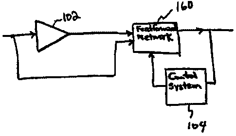
In addition, referring to FIGS. 18, 19, the
control system 104, 104' can also reduce distortion by
adjusting the characteristics of a feedforward network
160. As noted with regard to FIGS. 16 and 17, a
predistorer circuit can be advantageously used to further
reduce unwanted distortion components under the control
of, for example, a microprocessor. Referring to FIG. 20,
an amplification system 161 is illustrated which reduces
out-of-band frequency components of an input signal over
line 101 which after passing through Class A/B amplifier
102 has both in-band frequency components and out-of-band
frequency components. The amplification system includes
CA 02286531 1999-10-18
- 17 -
a feedfoward network 160 having a combiner 162 that
receives a pair of signals: the first signal (FIG. 6A)
over a line 161 from delay element 161a having the in-
band frequency components and a second signal (FIG. 6B)
over a line 163 coupled to the amplifier 102 output, that
has both in-band and out-of-band frequency components.
Optimally, the combiner 162 subtracts the first signal
from the second signal to produce a signal having only
out-of-band frequency components. A variable gain-phase
network 164, 166 receives the output of the combiner 162
and applies its output to an error amplifier 168.
Amplifier 168 amplifies the out-of-band frequency
components. A second combiner 170 adds the output of
amplifier 168 (that is, a signal having out-of-band
distortion components shifted by 180 ) to the signal
having both out-of-band and in-band frequency components
from a delay 169. Ideally, combiner 170 produces an
amplified signal substantially free of out-of-band
distortion components as is well known in the field.
However, as mentioned above, changes in the
feedforward network 160 components and the amplifier 102,
over time, can reduce the effectiveness of the
feedforward network 160 in reducing distortion. Thus,
the output of combiner 170 is coupled, in part, by a
coupler 171 to a feedback loop having control system 104.
The control system 104, described previously, detects
energy in the out-of-band frequency components and
produces a feedback control signal related to the
measured energy in those out-of-band frequency
components. The feedback control signals are coupled to
and adjust, in this illustrated embodiment, the
characteristics of the gain-phase network 164, 166 in
accordance with out-of-band frequency components.
As noted above, a predistortion circuit, as
illustrated in FIGS. 5 and 12, can be advantageously used
CA 02286531 1999-10-18
- 18 -
to further reduce unwanted distortion components under
the control of, for example, the microprocessor 122 of
FIG. 20. In addition, regarding both the illustrative
examples of FIGS. 19 and 20, the microprocessor 122 can
be used to adjust bias parameters of a predistorter, main
amplifier 102, gain-phase circuities or other devices to
advantageously reduce distortions in the amplified output
signal.
Referring now to FIG. 21, the control system 104
or 104' can control multiple components of an amplifier
system to produce an overall reduced distortion amplified
output signal. As shown, the control system 104 controls
the predistorter 105, the bias point of the main
amplifier 102, and the characteristics of the feedforward
network 106. Thus, different individual amplification
system networks (for example, the predistorter) combine
to form a larger network (that is, predistorter and
amplifier and feedforward network) having adjustable
characteristics adjustably controlled by the control
system in response to detected energy in the out-of-band
frequency components.
Throughout this discussion it has been implicitly
assumed that the input signal on line 101 was a single
channel, bandwidth limited signal having a carrier
frequency which was not known in advance. The distortion
compensation circuitry described in connection, for
example, with FIGS. 7 and 20, can also be employed when
the input signal is a multi-channel signal, each channel
having a bandwidth limited signal. When used with multi-
channel inputs, the compensation system finds one
channel, and minimizes the out-of-band frequency
components for that channel as if the other channel(s)
did not exist. Thereafter, the settings used for the one
channel are used for all of the channels.
CA 02286531 1999-10-18
- 19 -
Thus the operative structure and method of
operation of the FIGS. 7 and 20 embodiments remain the
same. It further appears not to matter which channel was
minimized so that the frequency generator 126 search
pattern, established by microprocessor 124 can be the
same as for a single channel, that is, for example, can
be a linear or a random sweep.
Additions, subtractions, and other modifications
of the disclosed embodiments will be apparent to those
practiced in the field and are within the spirit and
scope of the appended claims.
What is claimed is: