Note: Descriptions are shown in the official language in which they were submitted.
WO 93/17390 CA 02286992 1999-11-03 PCT/L'S92/0963t
- 1 -
This application is a divisional of Canadian Patent
Application Serial No. 2,130,433 filed November 5, 1992.
PROGRAMMABLE ELECTRICAL ENERGY METER AND METHODS THEREFOR
Field of Invention:
The present invention relates generally to the field
of utility company meters for metering electrical energy.
More particularly, the present invention relates to both
electronic watthour meters,and meters utilized to meter real
and reactive energy in both the forward and reverse
directions.
HackQround of the Invention:
Meters for metering the various forms of electrical
energy are well known. Utility company meters can be of three
general types, namely, electro-mechanical based meters (output
generated by a rotating disk), purely, electronic component
based meters (output component generated without any rotating
parts) and a hybrid mechanical/ealectronic meter. In the
hybrid meter, a so-called electronic register is coupled,
usually optically, to a rotating disk. Pulses generated by
the rotating disk, for example by :Light reflected from a spot
painted on the disk, are utilized to generate an electronic
output signal. -
It will be appreciatedthat the use of electronic
components in electric energy meters has gained considerable
.acceptance due to their reliabi7.ity and extended ambient
temperature ranges of operation. Moreover, contemporary
electronic signal processing devices, such as microprocessors,
have a greater accuracy potential for calculating electrical
energy use than prior mechanical. devices. Consequently,
various forms of electronic based meters have been proposed
CA 02286992 1999-11-03
-2-
which are virtually free of any moving parts. Several meters have been
proposed
which include a microprocessor.
U.S. Patent No. 4,298,839 - Johnston, discloses a programmable alternating
current electric energy meter having a radiation responsive external data
interface.
The meter is shown to include a metering sequence logic control circuit which
in
the preferred embodiment is stated to be formed by a single-chip
microcomputer,
type MK 3870 available from Mostek Corporation of Carrollton, Texas. The logic
control circuit is said to be operative to calculate and accumulate different
measured parameters of an electrical energy quantity. Current and voltage
components are provided to the logic control circuit from a converter which
produces current and voltage pulses at a rate proportional to the rate of the
particular electrical energy consumed. The converter incorporates a rotating
disk.
U.S. Patent No. 4,467,434 - Hurly et al, discloses a solid-state watt-hour
meter which includes a current sensing device and a voltage sensing device
coupled to a Hall-effect sensing and multiplying device. The Hall-effect
device is
coupled to a microprocessor.
U.S. Patent No. 4,692,874 - Mihara, discloses an electronic watt-hour meter
which includes a single microprocessor and a power measuring device. The
power measuring device is described as including an electric power converting
circuit and a frequency divider. The electric power converting circuit
provides an
output pulse, the frequency of which is divided by the frequency divider. The
frequency divider, however, is dependent upon a frequency dividing, ratio
setting
signal generated by the microprocessor.
U.S. Patent No. 4,542,469 - Brandyberry et al, discloses a hybrid type
meter having a programmable demand register with a two-way communication
optical port. The demand register is said to include a central processing unit
such
as the NEC 7503 microcontroller. The microcontroller is
WO 93/17390 ca o22s6992 1999-ii-03 p~/US92109631
- 3 -
utilized not only for controlling and monitoring the demand
register, but also to perform power and energy calculations.
U.S. Patent No. 4,884,.021 - Hammond et al.
discloses a meter for metering polyphase power sources wherein
cycles for each phase are sampled at each degree and converted
to a binary representation of amplitude. Conversion is
described as being carried out i.n two steps, the first being
a range conversion where the sampled amplitude is evaluated
with respect to eleven possible ranges of amplitude or scaling
factors. That range data is then stored and the sample is
amplified in accordance with l~he desired range code and
submitted to an analogue to digital converter. A general
purpose digital signal processor- is said to be utilized for
treating the parameters derived from each sample and to
develop pulse outputs which can be further processed or
displayed by devices of conventional use in the industry. An
electronic register is provided which is said to be controlled
by a conventional microprocessor. The implementation of
Hammond's range conversion scheme results in the energy
measurement components effectively being "hard coded" with the
particular metering scheme, thereby significantly reducing the
adaptability of the meter for various known applications. The
use of such a meter in then various utility company'
applications requires either keeping several different meter
types in inventory, i.e. one meter type for each type of
application, or one meter into which all application forms
have been incorporated. It will be appreciated that one meter
into which all application forms have been incorporated would
be exorbitantly expensive.
Meters, such as thoae described above, which
incorporate registers, are generally programmable at two
levels. At the first level, firmware can be masked into a
register in a relatively short period of time. At the second
level, so-called soft switches c:an be programmed into non-
volatile memory, i.e., electrcally erasable programmable read
only memory, to tell the firmware which algorithms to perform.
Such systems work well for presently provided base metering
WO 93/17390 CA 02286992 1999-ii-o3 p~/b~s92/09631
data. However, such systems cannot change basic meter
functions nor are they adaptable to use with additional
hardware. While adequate for present applications, such
metering systems are significantly non-flexible in relation
to future needs and/or developments in both hardware and
programmability.
U.S. Patent No. 4,07',),061 - Johnston et al.
discloses a digital processing and. calculating AC electric
energy metering system. This system includes a single central
l0 processing unit for performing all energy determinations,
system control and information display. Although this system
does provide energy determination as output signals from the
system, the system is not adaptable=_ for modification of basic
metering functions from external lhardware or in relation to
external communication signals.
Consequently, a need exits for an electronic meter
which is designed to be programmab:Le to the extent that basic
metering functions can be changed z-elatively easily and which
is economically adaptable for use with additional hardware.
Such a meter would be capable of modification to handle
various meter forms, to store calibration constants and to be
capable of modification for future metering requirements. The
present invention solves the aforementioned problems through
the use of a distributed processing electronic meter
incorporating a metering processor which is adaptable to
multiple metering applications and which is utilized to
perform all electrical energy determinations and a second
processor which generates a display signal based on such
electrical energy determinations, serves to control the
overall operation of the meter and~which provides access to
processing, storage and display information for future
hardware additions.
6ummary of the Invention:
The above problems are o~rercome and the advantages
of the invention are achieved in methods and apparatus for
metering electrical energy in an electronic meter. Such meter
includes a first processor for determining electrical energy
CA 02286992 2004-06-02
- 5 -
from voltage and current signals and for generating an
energy signal representative of the electrical energy
determination and a second processor for receiving the
energy signal and for generating an indication signal
representative of said energy' signal. An option connector
is connected to the first and second processors, whereby the
energy signal is provided to the option connector and a
communication connection is provided between the option
connector and the second processor. It is preferred for the
option connector to be provided power signals such used by
the meter in order to power any electrons c components which
may be connected to the option connector. It is also
preferred to provide the option connector with certain
operation signals such as a power fail signal, a master
reset signal, an end of demand signal, and a KYZ signal. It
is still further preferred to provide the option connector
with the potential to communicate with various components of
the meter, such as serial data communication, communication
signals transmitted and received through an optical port and
display signals. It is also preferred for the first
processor to include a comparator, connected to receive a
precision voltage and a reference voltage, wherein a
comparator signal is generated whenever the reference
voltage exceeds the precision voltage, It is also preferred
for the meter to include a non-volatile memory such as an
electrically erasable programmable read only memory
connected to the first and second processors, for storing
data used by the processors and for storing information
generated by the processors.
According to one broad aspect of the present
invention, there is provided a method of metering
electrical energy comprising the steps of: sensing each
phase of a circuit to generate analog voltage signals and
analog current signals associated with each phase;
converting the analog voltage signals and the analog
current signals into digital voltage signals and digital
current signals, respectively, using time division
multiplexing to provide three digital
CA 02286992 2004-06-02
- 5 A -
outputs, each digital output comprising at least one
digital voltage signal ar~d at least one digital current
signal associated with the same phase; and processing the
digital outputs to generate signals representative of real
power, the magnitude of reactive power, and apparent power,
wherein the signals representative of the magnitude of
reactive power are generated from the signals
representative of real power and the signals representative
of apparent power.
Brief Description of the Drawings:
The present invention will be better understood,
and its numerous objects and advantages will become apparent
to those skilled in the art by reference to the following
detailed description of the invention when taken in
conjunction with the following drawings, in which:
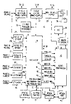
Fig. 1 is a block diagram of an electronic meter
constructed in accordance with the present invention;
WO 93/I7390 CA 02286992 1999-ii-o3 - p~/L~S92/09631
- 6 -
Fig. 2 is a block diagram of the A/D&DSP processor
shown in Fig. 1;
Figs. 3A-3E combine to ;provide a flow chart of the
primary program utilized by the m:icrocontroller disclosed in
Fig. 1;
Fig. 4 is a flow chart of the download program
utilized by the microcontroller shown in Fig. 1;
Fig. 5 is a schematic diagram of the optical port
disclosed in Fig. 1;
Fig. 6 is a schematic diagram of the resistive
dividers and precision reference disclosed in Fig. 1.
Fig. 7 is a schematic diagram of the 5 volt linear
power supply shown in Fig. 1; and
Fig . 8 is a schematic diagram of various electronic
button switches utilized by the mic:rocontroller shown in Fig.
1.
Detailed Description:
A new and novel meter for metering electrical energy
is shown in Fig. 1 and generally designated 10. It is noted
at the outset that this meter is. constructed so that the
future implementation of higher level metering functions can
be supported. Such future implementation feature is described
in greater detail herein.
Meter 10 is shown to include three resistive voltage
divider networks 12A, 12B, 12C; a first processor - an ADC/DSP
(analog-to-digital converter/digital signal processor) chip
14; a second processor - a microcontroller 16 which in the
preferred embodiment is a Mitsubishi Model 50428
microcontroller; three current sensors 18A, 18B, 18C; a 12V
switching power supply 20 that is capable of receiving inputs
in the range of 96-528V; a 5V linear power supply 22; a non-
volatile power supply 24 that switches to a battery 26 when
5V supply 22 is inoperative; a 2.5V precision voltage
reference 28; a liquid crystal display (LCD) 30; a 32.768 kHz
oscillator 32; a 6.2208 MHz oscillator 34 that provides timing
signals to chip 14 and whose signal is divided by 1.5 to
provide a 4.1472 MHz clock signal to microcontroller 16; a 2
WO 93/17390 CA 02286992 1999-ii-o3 PCT/US92/09631
kByte EEPROM 35; a serial communications line 36; an option
connector 38; and an optical communications port 40 that may
be used to read the meter. The inter-relationship and
specific details of each of these components is set out more
fully below.
It will be appreciated that electrical energy has
both voltage and current characteristics. In relation to
meter 10, voltage signals are provided to resistive dividers
12A-12C and current signals are induced in a current
transformer (CT) and shunted. The output of CT/shunt
combinations 18A-18C is used to determine electrical energy.
First processor 14 is connected to receive the
voltage and current signals provided by dividers 12A-12C and
shunts 18A-18C. As will be explained in greater detail below,
processor 14 converts the voltage and current signals to
voltage and current digital signals, determines electrical
energy from the voltage and current digital signals and
generates an energy signal representative of the electrical
energy determination. Processor 14 will always generate
watthour delivered (Whr Del) and watthour received (Whr Rec)
signals, and depending on the type of energy being metered,
will generate either volt amp reactive hour delivered (VARhr
Del)/volt amp reactive hour received (VARhr Rec) signals or
volt amp hour delivered (VAhr Del)/volt amp hour received
(VAhr Rec) signals. In the preferred embodiment, each
transition on conductors 42-48 (each transition from logic low
to logic high or vice versa) is representative of the
measurement of a unit of energy. Second processor 16 is
connected to first processor 14. As will be explained in
greater detail below, processor 16 receives the energy
signals) and generates an indication signal representative
of the energy signal.
In relation to the preferred embodiment of meter 10,
currents and voltages are sensed using conventional current
transformers (CT's) and resistive voltage dividers,
respectively. The appropriate multiplication is accomplished
in a new integrated circuit, i.e. processor 14. Although
WO 93/17390 ca o22s6992 1999-ii-03 p~-/LrS9Z/U9631
g -
described in greater detail in relation to Fig. 2, processor
14 is essentially a programmable digital signal processor
(DSP) with built in analog to digital (A/D) converters. The
converters are capable of sampT.ing three input channels
simultaneously at 2400 Hz each with a resolution of 21 bits
and then the integral DSP performs various calculations on the
results.
Meter 10 can be operated as either a demand meter
or as a so-called time of use (TOU) meter. It will be
recognized that TOU meters are becoming increasingly popular
due to the greater differentiation by which electrical energy
is billed. For example, electrical energy metered during peak
hours will be billed differently than electrical energy billed
during non-peak hours. As will be explained in greater detail
below, first processor 14 determines units of electrical
energy while processor 16, in the ToU mode, qualifies such
energy units in relation to the time such units were
determined, i.e. the season as well as the time of day.
All indicators and tast features are brought out
through the face of meter 10, either on LCD 30 or through
optical communications port 40. Power supply 20 for the
electronics is a switching power :supply feeding low voltage
linear supply 22. Such an approach allows a wide operating
voltage range for meter 10.
In the preferred embodiment of the present
invention, the so-called standa~__~d meter components and
register electronics are for the first time all located on a
single printed circuit board (not shown) defined as an
electronics assembly. This electronics assembly houses power
supplies 20, 22, 24 and 28, resistive dividers 12A-12C for all
three phases, the shunt resistor portion of 18A-18C,
oscillator 34, processor 14, procsasor 16, reset circuitry
(shown in Fig. 8), EEPROM 35, oscillator 32, optical port
components 40, LCD 30, and an option board interface 38. When
this assembly is used for demand metering, the billing data
is stored in EEPROM 35. This same assembly is used for TOU
WO 93/17390 CA 02286992 1999-ii-03 PCT/US92/09631
g
metering applications by merely utilizing battery 26 and
reprogramming the configuration data in EEPROM 35.
Consider now the various components of meter 10 in
greater detail. Primary current being metered is sensed using
conventional current transformers. It is preferred for the
current transformer portion of devices 18A-18C have tight
ratio error and phase shift specifications in order to limit
the factors affecting the calibration of the meter to the
electronics assembly itself. :~uch a limitation tends to
enhance the ease with which meter 10 may be programmed. The
shunt resistor portion of devicesc 18A-18C are located on the
electronics assembly described above and are preferably metal
film resistors with a maximum temperature coefficient of 20
ppm/°C.
The phase voltages are brought directly to the
electronic assembly where resistive dividers 12A-12C scale
these inputs to processor 14. I:n the preferred embodiment,
the electronic components are referenced to the vector sum of
each line voltage for three wire delta systems and to earth
ground for all other services. Rsaistive division is used to
divide the input voltage so that a very linear voltage with
minimal phase shift over a wide dynamic range can be obtained.
This in combination with a switching power supply allows the
wide voltage operating range to be implemented.
Referring briefly to Fic~. 6, each resistive divider
consists of two 1 Meg, 1/2 watt resistors 50/52, 54/56 and
58/60, respectively. Resistors 50-60 are used to drop the
line voltage at an acceptable watt loss. Each resistor pair
feeds a third resistor 62, 64 and E.6, respectively. Resistors
62-66 are metal film resistors having a maximum temperature
coefficient of 25 ppm/°C. Z'his combination is very
inexpensive compared to other voltage sensing techniques.
Resistors 50-60 have an operating voltage rating of 300 Vans
each. These resistors have been individually tested with the
6 kV IEEE 587 impulse waveforms to assure that the resistance
is stable and that the devices are not destroyed. Resistors
62-66 scales the input voltage to be less than 1 Volt peak to
CA 02286992 1999-11-03
- 10-
peak to processor 14. It is noted that resistors 62-66 can be in a range from
about
100 ohms to about 1 k ohms in order to assure this maximum peak to peak
voltage
and still maintain maximum signal.
On grounded, three wire delta systems, l:hose components of the electronics
assembly operating on logic voltage levels (including the battery connector)
can
be at an elevated voltage. In such situations, the rivo, 1 Meg resistor
combinations
(50/52, 54/56, 58/60) provide current limiting to the logic level electronics.
The
worse case current occurs during testing of a 480 V, 3 wire delta meter with
single
phase excitation. -
It will be appreciated that energy units are calculated primarily from
multiplication of voltage and current. The specific formulae utilized in the
preferred embodiment are listed in Table 1. This especially preferred
embodiment
allows four wire delta applications to be metered using a four wire wye meter
executing the four wire wye equations in Table; 1. However, for purposes of
Fig.
2, such formulae are performed in processor 14. Processor 14 includes an
analog
converter 70 and a programmable DSP 72. l~onverter 70 includes three three-
chanel, over-sampled, 2nd order, sigma-delta A/D converters, depicted as a 9
channel EO analog-to-digital converter 74. The 6.2208 MHz clock signal is
divided by 3 such that each A/D samples its input at 2.0736 MHz. Each A/D
performs a 96:1 reduction or averaging for each input that results in an
effective
sample rate of 2.4 kHz on each of the three inputs per A/D. The resolution of
these samples is equivalent to 21 bits, plus sign.. It is noted that such a EO
analog-
to-digital conversion scheme results in a correct convergence by each A/D for
each sample converted. It is recognized that the bandwidth for such a
conversion
scheme is relatively small, however, the frequency of the voltage and current
being converted is also relatively small.
WO 93/I 1390 CA 02286992 1999-m-o3 p['f/L,'S92/09631
li ~-
In the preferred embodiment, the three voltage
inputs, Va, Vb and Vc are sampled by one of the A/D's and the
three current inputs Ia, Ib and Ic are sampled by a second
A/D. The third A/D is used to sample either the voltage or
current input of the B phase. Such sampling of the voltage
or current input of the B phase is done because so-called 2
1/2 element meters require the combination of the B phase
current with one or both of the other phase currents. In
addition, so-called two element meters require the B phase
l0 voltage to be combined with the other phase voltages to
produce the line to line voltage. Having a third A/D enables
these terms to be sampled simultaneously, thereby improving
the measurement accuracy. This also improves the signal to
noise ratio within processor 14.
DSP 72 is a reduced instruction set processor (RISC)
which computes the desired energy quantities from the
converted voltage and current samples . DSP 72 is shown to
include a random access memory (RAM) memory 76 having a
capacity of 256 bytes of data. Memory 76 is used to store
computations and the subroutine stack. A read only memory
(ROM) 78 is also shown and has a capacity of 640 bytes of
data. Memory 78 is used to store those metering subroutines
common to all energy calculation,. Another RAM memory 80 is
depicted and has a capacity of 256 bytes of data. Memory 80
- 25 is used to store the main line program and specialized
subroutines of DSP 72.
DSP 72 is also shown tc~ include multiplier 82 and
an accumulator 84 for processing the voltage and current
digital signals thereby generating electrical energy
information. There is also included arithmetic subtraction
unit 86 interposed between multiplier 82 and accumulator 84.
From the foregoing, it should be appreciated that
program ROM, i.e. .memory 76 '.s defined at the oxide via level.
As this defining step :.~ccurs relatively late in the
manufacturing process for processor 14, changes can be made
to such programming with minimal effort.
WO 93/17390 CA o22s6992 1999-ii-03 p~'/[,~Sg2/09631
- 12 -
Calibration constants for each phase and certain
potential linearization constants are stored in memory 80.
Memories 76 and 80 are serially down-loaded from EEPROM 35 by
microcontroller 16 on power-up of meter 10. Such an
embodiment allows the benefit of being able to provide various
meter forms economically, to calibrate without hardware
modification, and permits the future addition of metering VAR
or VA based on the per phase Vans and Irms. The formulae for
such operations are included in 'Table 1. Furthermore, the
calculation of future, yet undefined, complex metering
quantities could be obtained by merely reprogramming processor
14.
Processor 14 also contains a crystal oscillator (not
shown), serial interface 88, power fail detect circuitry 90,
and potential present outputs B and C. The crystal oscillator
requires an external 6.2208 MHz crystal oscillator 34.
Processor 14 uses this frequency directly for driving the DSP
and indirectly for the A/D sampling. This frequency is also
operated upon by clock generator 92. which serves to divide the
output of oscillator 34 (input to processor 14 at XIN and
ROUT) by 1.5, to buffer the divided clock signal and to output
the divided clock signal at CK to processor 16 as its clock.
This clock output is specified 1.o work down to a supply
voltage of 2.0 VDC.
Serial interface 88 is a derivation of the Signetics
IIC bus. One serial address is assigned to processor 14.
This address accesses one of the lour DSP control registers.
All information must pass through ;DSP data register 94 after
writing the DSP address register. All memory, registers, and
outputs of processor 14 can be read serially. A chip select
line CS has been added to disable i~he communications buffer.
The input CS is connected to and controlled by processor 16:
Power fail detection circuit 90 is a comparator
which compares a divided representation of the supply voltage
to a precision reference. The comparator's output at A
concurrently provides a power fail signal and an indication
of the presence of A phase voltage. Upon power fail, it is
WO 93/17390 ca o22s6992 1999-ii-03 PCT/L,'S92/09631
- 13 -
preferable to reset processor 14. In such a situation, the
output pins Whr, Whd, etc. are forced to logic low voltage
levels. Additionally, processor- 14 goes into a lower power
mode to reduce the current draw on power supply 20. In this
lower power mode the comparator and oscillator operation are
not affected, but DSP 72 ceases to operate.
The power failure voltage PF is generated by
dividing the output of supply 22 to generate a voltage which
is slightly greater than 2.5V. In the preferred embodiment,
a resistor voltage divider provides PF. Since PF is generated
in relation to the Phase A voltage (Fig. 1), its presence is
an indication that the Phase A voltage is also present.
In order to appreciate how the reference voltage is
generated consider Fig. 7. There is shown in greater detail
the components included in linear power supply 22. The 5V
output of supply 22 is provided at 96 in Fig. 6. Resistor 98
and diode 100 combine to generate a precision 2.5V reference
voltage. It is noted at this pc>int that Va, Vb, Vc, Ia, Ib
and Ic are each provided to proca;ssor 14 in reference to VREF.
Consider again processor 14 as shown in Fig. 2. The
phase B and C potential indicators outputs are under control
of DSP 72. The B output is normally a logic level output.
The C output also provides the power line time base function
(note that phase C is present in all applications). To
minimize noise at the power line fundamental, this time base
is at two times the power line fundamental.
The M37428 microcontroller 16 is a 6502 (a
traditional 8 bit microprocessor) derivative with an expanded
instruction set for bit test and manipulation. This
microcontroller includes substant:.ial functionality including
internal LCD drivers (128 quadraplexed segments), 8 kbytes of
ROM, 384 bytes of RAM, a full duplex hardware UART, 5 timers,
dual clock inputs (32.768 kHz a:nd up to 8 MHz), and a low
power operating mode.
During normal operation, processor 16 receives the
4.1472 MHz clock from processor 7.4 as described above. Such
a clock signal translates to a 1.0368 MHz cycle time. Upon
WO 93/17390 ~ CA 02286992 1999-ii-03 p~/US92/09631
- 14 -
power fail, processor 16 shifts to the 32.768 kHz crystal
oscillator 32. This allows low power operation with a cycle
time of 16.384 kHz. During a power failure, processor 16
keeps track of time by counting ss:conds and rippling the time
forward. Once processor 16 has rippled the time forward, a
WIT instruction is executed which places the unit in a mode
where only the 32.768 kHz oscillator and the timers are
operational. While in this mode a timer is setup to "wake up"
processor 16 every 32,768 cycles to count a second.
Consider now the main operation of processor 16 in
relation to Figs. 3A-3E and Fig. 4. At step 1000 a reset
signal is provided to microcontroller 16. As will be
appreciated in relation to the discussion of Fig. 5, a reset
cycle occurs whenever the voltage level V~ rises through
approximately 2 . 8 volts . Such a condition occurs when the
meter is first powered up.
At step 1002, microcontroller 16 performs an
initialize operation, wherein the stack pointer is
initialized, the internal ram is initialized, the type of
liquid crystal display is entered into the display driver
portion of microcontroller 16 and timers which require
initialization at power up are initialized. It will be noted
that the operation of step 1002 does not need to be performed
for each power failure occurrence. Following a power failure,
microcontroller 16 at step 1004 r~sturns to the main program
at the point indicated when the power returns.
Upon initial power up cr the return of power after
a power failure, microcontrolle:r 16 performs a restore
function. At step 1006, microconltroller 16 disables pulses
transmitted by processor 14. These pulses are disabled by
providing the appropriate signal restore bit. The presence
of this bit indicates that a restore operation is occurring
and that pulses generated during that time should be ignored.
Having set the signal restore bit, microcontroller 16
determines at step 1008 whether the power fail signal is
present. If the power fail signal is present, microcontroller
16 jumps to the power fail routine at 1010. In the power fail
WO 93/17390 CA 02286992 1999-ii-o3 PCT/US92/09631
- 15 -
routine, the output ports of microcontroller 16 are w=itten
low unless the restore bit has not been set. If the restore
bit has not been set, data in the microcontroller 16 is
written to memory.
If the power fail signal is not present,
microcontroller 16 displays segments at step 1012. At this
time, the segments of the display are illuminated using the
phase A potential. It will be recalled that phase A potential
is provided to microcontroller lE~ from processor 14. At 1014,
the UART port and other ports are initialized at 1016, the
power fail interrupts are enabled such that if a falling edge
is sensed from output A of processor 14, an interrupt will
occur indicating power failure. It will be recalled that
processor 14 compares the refere;zce voltage VREF to a divided
voltage generated by the power supply 20. Whenever the power
supply voltage falls below the reference voltage a power fail
condition is occurring.
At step 1018, the downloading of the metering
integrated circuit is performed. Such downloading operation
is described in greater detail in relation to Fig. 4. At step
1020, the timer interrupts are enabled. It will be
appreciated that certain tasks performed by microcontroller
16 are time dependent. Such tasks will require a timer
interrupt when the time for performing such tasks has arrived.
At 1022, the self-test: subroutines are performed.
Although no particular self-tests subroutine is necessary in
order to practice the present invention, such subroutines can
include a check to determine if proper display data is
present. It is noted that data i;s stored in relation to class
designation and that a value is assigned to each class such
that the sum of the class value: equals a specified number.
If any display data is missing, the condition of the class
values for data which is present will not equal the specified
sum and an error message will be displayed. Similarly,
microcontroller 16 compares the: clock signal generated by
processor 14 with the clock signal generated by watch crystal
WO 93/17390 Ca o22s6992 1999-ii-03 p~/L~S92/09631
- 16 ~-
32 in order to determine whether 'the appropriate relationship
exists.
Having completed the self-test subroutines, the ram
is re-initialized at 1024. In this re-initialization, certain
load constants are cleared from memory. At 1026, various
items are scheduled. For example, the display update is
scheduled so that as soon as the restore routine is completed,
data is retrieved and the display is updated. Similarly,
optical communications are scheduled wherein microcontroller
16 determines whether any device is present at optical port
40, which device desires to communicate. Finally, at 1028 a
signal is given indicating that the restore routine has been
completed. Such a signal can include disabling the signal
restore bit. Upon such an occurrence, pulses previously
disabled will now be considered valid. Microcontroller 16 now
moves into the main routine.
At 1030, microcontroller 16 calls the time of day
processing routine. In this routine, microcontroller 16 looks
at the one second bit of its internal and determines whether
the clock needs to be changed. Fo:r example, at the beginning
and end of Daylight Savings Time, the clock .is moved forward
and back one hour, respectively. I:n addition, the time of day
processing routine sets the minute change flags and date
change flags. As will be appreciai:ed hereinafter, such flags
are periodically checked and processes occur if such flags are
present.
It will be noted that there are two real time
interrupts scheduled in microcontroller 16 which are not shown
in Fig. 3, namely the roll minute interrupt and the day
interrupt. At the beginning of every minute, certain minute
tasks occur. Similarly, at the beginning of every day,
certain day tasks occur. Since such tasks are not necessary
to the practice of the presently claimed invention, no further
details need be provided.
At 1032, microcontrollex- 16 determines whether a
self-reprogram routine is scheduled. If the self-reprogram
routine is scheduled, such routine: is called at 1034. The
WO 93/17390 CA 02286992 1999-ii-03 PCT/LJS92/09631
Z7
self-reprogram typically programs in new utility rates which
are stored in advance. Since new rates have been
incorporated, it will be necessary to also restart the
display. After operation of i~he self-reprogram routine,
microcontroller 16 returns to the main program. If it is
determined at 1032 that the self-reprogram routine is not
scheduled, microcontroller 16 dei~ermines at 1036 whether any
day boundary tasks are scheduled. Such a determination is
made by determining the time and day and searching to see
whether any day tasks are scheduled for that day. If day
tasks are scheduled, such tasks a:re called at 1038. If no day
tasks are scheduled, microcontroller 16 next determines at
1040 whether any minute boundary tasks have been scheduled.
It will be understood that since: time of use switch points
occur at minute boundaries, far example, switching from one
use period to another, it will be necessary to change the data
storage locations at such a point. If minute tasks are
scheduled, such tasks are called .at 1042. If minute boundary
tasks have not been scheduled, microcontroller 16 determines
at 1044 whether any self-test have been scheduled. The self-
tests are typically scheduled to occur on the day boundary.
As indicated previously, such sell.°-tests can include checking
the accumulative display data class value to determine whether
the sum is equal to a prescribed. value. If self-tests are
scheduled, such tests are called at 1046. If no self-tests
are scheduled, microcontroller 16 determines at 1048 whether
any season change billing data copy is scheduled. It will be
appreciated that as season changes billing data changes.
Consequently, it will be necessary for microcontroller 16 to
store energy metered for one season and begin accumulating
energy metered for the following season. If season change
billing data copy is scheduled, such routine is called at
1050. If no season change: routine is scheduled,
microcontroller 16 determines at 1052 whether the self-
redemand reset has been scheduled. ~ If the self-redemand reset
is scheduled, such routine is called at 1054. This routine
requires microcontroller 16 to in effect read itself and store
WO 93/17390 CA 02286992 1999-ii-o3 - p~-/~lSgW09631
- 18 -
the read value in memory. The demand reset is then reset.
If the self-demand reset has not been scheduled,
microcontroller 16 determines at 1.056 whether a season change
demand reset has been scheduled. If a season change demand
reset is scheduled, such a routine is called at 1058. In such
a routine, microcontroller 16 reads itself and resets the
demand.
At 1060, microcontroller 16 determines whether
button sampling has been scheduled. Reference is made to Fig.
8 for a more detailed description of an arrangement of buttons
to be positioned on the face of meter l0. Button sampling
will occur every eight milliseconds. Consequently, if an
eight millisecond period has passed, microcontroller 16 will
determine that button sampling is. scheduled and the button
sampling routine will be called at: 1062.
If button sampling is not scheduled, microcontroller
16 determines at 1064 whether a display update has been
scheduled. This routine causes a new quantity to be displayed
on LCD 30. As determined by 'the soft switch settings
mentioned above, display updates a:re scheduled generally for
every three-six seconds. If the display is updated more
frequently, it may not be possible to read the display
accurately. If the display update has been scheduled, the
display update routine is called at 1066.
If a display update has not been scheduled,
microcontroller 16 determines at 1068 whether an annunciator
flash is scheduled. It will be recalled that certain
annunciators on the display are made to f l ash . Such f lashing
typically occurs every half second. If an annunciator flash
is scheduled, such a routine is .called at 1070. If no
annunciator flash is scheduled, microcontroller 16 determines
at 1072.whether optical communication has been scheduled. It
will be recalled that every half :second microcontroller 16
determines whether any signal has been generated at optical
port. If a signal has been generated indicating that-optical
communications is desired, the optical communication routine
will be scheduled. If the optical communication routine is
WO 93/17390 ca o22s6992 1999-m-03 p~-/L,rS92/09631
- 19 -
scheduled, such routine is cal:Led at 1074. This routine
causes microcontroller 16 to ~~ample optical port 40 for
communication activity.
If no optical routine is scheduled, microcontroller
16 determines at 1076 whether processor 14 is signaling an
error. If processor 14 is signaling an error, microcontroller
16 at 1078 disables the pulse deaection, calls the download
routine and after performance of that routine, re-enables the
pulse detection. If processor 14 is not signaling any error,
l0 microcontroller 16 determines at. 1080 whether the download
program is scheduled. If the download program is scheduled,
the main routine returns to 1078 and thereafter back to the
main program.
If the download program has not been scheduled or
after the pulse detect has been re-enabled, microcontroller
16 determines at 1082 whether a warmstart is in progress. If
a warmstart is in progress, the power fail interrupts are
disabled at 1084. The pulse computation routine is called
after which the power fail interrupts are re-enabled. It will
be noted that in the warmstart data is zeroed out in order to
provide a fresh start for the meter. Consequently, the pulse
computation routine performs the necessary calculations for
energy previously metered and places that computation in the
appropriate point in memory. If a warmstart is not in
progress, microcontroller 16 at: 1084 updates the remote
relays. Typically, the remote relays are contained on a board
other than the electronics assembly board.
Referring now to Fig. 4, the program for downloading
processor 14 will be described. At 1100, microcontroller 16
enters the program. At 1102, the schedule indicating that a
metering download should take place is cleared. At 1104,
Microcontroller 16 initializes the communication bus, which
in the preferred embodiment is INTIB. At 1106, microcontroller
16 resets and stops processor by way of an interrupt on
processor 14. However, if there is a communications error
between microcontroller 16 and processor 14, microcontroller
16 at 1108 sets a warning and schedules a download of
WO 93/17390 CA 02286992 1999-11-03 - p ['t/L)g92/09631
p ..
processor 14. After 1108 the downloading program is
terminated, microcontroller 16 returns to the main routine.
At 1110, microcontroller reads and saves the pulse
line states. It will be recalledl that as processor 14 makes
energy determinations, each unit of energy is represented by
a logic transition on outputs 4:?-48 (Fig.l). At 1110 the
state of each output 42-48 is saved. At 1112, microcontroller
initializes A/D converters 74, if a communication error
occurs, microcontroller proceeds t:o 1108. At 1114 the digital
signal processing registers 94 are initialized. At 1116
program memory 78 is downloaded to memory. At 1118, the data
memory 80 is downloaded to memory. At 1120, processor 14 is
started. If a communication error occurs at any of steps
1114-1120, microcontroller 16 again returns to 1108. At 1122,
any warning messages previously sEat at 1108 are cleared. At
1124, microcontroller 16 returns i~o its main program.
All data that is considered non-volatile for meter
10, is stored in a 2 kbyte EF:PROM 35. This includes
configuration data (including the data for memory 76 and
memory 80), total kWh, maximum and cumulative demands (Rate
A demands in TOU) , historic TOU data, cumulative number of
demand resets, cumulative number of power outages and the
cumulative number of data altering communications. The
present billing period TOU data is ;stored in the RAM contained
within processor 16. As long as l:he microcontroller 16 has
adequate power, the RAM contents and real time are maintained
and the microcontroller 16 will not be reset (even in a demand
register).
As indicated previously, operational constants are
stored in EEPROM data. Microcontroller 16 performs checks of
these memory areas by adding the class designations for
various data and comparing the sum t:o a reference number. For
example, the data class is used to define the 256 byte block
of program memory. Appended to the 256 bytes of program in
this data class is the DSP code identification, revision
number, and the checksum assigned to this data class . The
operational constants consist of the calibration constants and
CA 02286992 1999-11-03
-21-
data RAM initial values, the meter's secondary Ke and Kh, and information that
the microcontroller must use to process the meter's data.
LCD 30 allows viewing of the billing and other metering data and statuses.
Temperature compensation for LCD 30 is provided in the electronics. Even with
this compensation, the meter's operating temperature range and the LCD's 5
volt
fluid limits LCD 30 to being triplexed. Hence, the maximum number of segments
supported in this design is 96. The display response time will also slow
noticeably
at temperatures below -30 degrees Celsius.
Referring now to Fig.S, optical port 40 and reset circuitry 108 are shown in
greater detail. On power up, reset 108 provides an automatic reset pulse to
processor 16. In operation, circuit 108 acts as a comparator, comparing a
portion
of the voltage generated by power supply 22 to the voltage provided by non-
volatile supply 24. Whenever the voltage generated by power supply 22 either
falls below or rises above that of the non-volatile supply, such a condition
is an
indication that the meter has either lost power or power has been restored and
a
reset signal is provided to processor 16.
Optical port 40 provides electronic acce:>s to metering information. The
transmitter and receiver (transistors 110 and 112) are 850 nanometer infrared
components and are contained in the electronics assembly (as opposed to being
mounted in the cover). Transistor 110 and LED 112 are tied to microcontroller
16's DART and the communications rate (9600 baud) is limited by the response
time of the optical components. The optical port can also be disabled from the
UART (as described below), allowing the UART to be used for other future
communications without concern about ambient light. During test mode, the
optical port will
CA 02286992 1999-11-03 p~'/(JS92/09631
WO 93/17390
- 22 -
echo the watthour pulses received by the microcontroller over
the transmitting LED 112. While in test mode microcontroller
16 will monitor the receive line 114 for communications
commands.
One feature which results from the distributed
processing scheme described above is the adaptability or
expandability of the invention in future applications. To
this end, option connector 38 will play a key role. As shown
in Fig. 1, option connector provides a connection from
processor 16 to the outside world. Through connector 38 data
output from processor 14 to EEPFtOM 35 or data output to
processor 16 can be monitored. A:~ will be described below,
communication with processor 16 can occur since connector 38
is directly connected to several ports on processor 16. Thus
through option connector 38, communication with processor 16
is possible and the operation of processor 16 may be modified.
For example, connector 38 may be used in order to convert
meter 10 effectively into a peripheral device for another
microcontroller (not shown). option connector 38 might be
used in relation to a modem in order to access pieces of data
or to operate optical port 40 in some desired fashion.
Connector 38 may also be used in relation to so called 3rd
party services. In such situations, third parties may be
contracted to service the meter using their own equipment.
Through connector 38 it may be possible to more readily adapt
such equipment to be capable of servicing meter 10. Connector
38 may also be utilized for the connection of a device for the
storage of an energy use profile. Such devices require non-
volatile supply voltages. The features made available on
connector 38 makes it possible to "piggy-back" such a device
on meter 10.
As indicated above, it i;s desirable for meter 10 to
economically perform existing polyphase demand and time-of-use
(TOU) metering as well as be the p7.atform for future metering
products. Unfortunately, little :is known about the future.
The problem therefore is how one gallows for the changes the
future might bring. The approach taken by the invention,
WO 93/17390 CA 02286992 1999-ii-o3 p~/US92/09631
- 23 -
allows the electronics in meter 10 to act as a peripheral
device to an option board (not shown) connected to option
connector 38, while supplying nominal power requirements for
the option board. All power, signals, and communications to
the option board are provided over a 20 pin connection.
Meter 10 provides the following power signals:
V+ A semi-regulated l2VDC to lSVDc supply (the
output of supply 20);
5V A regulated SV vo:latile supply (the output of
supply 22);
VDD A regulated 5V non-volatile supply (the output
of supply 24); and
Gnd The negative reference.
In the preferred emboc!iment, the option board is
allowed a combined current draw of 50mA on these three supply
signals. The option board can be allowed to draw up to 100~A
from a supercapacitor contained in the output portion of
supply 20 and battery 26 via supply 24 during a power outage,
however, such an arrangement will. reduce battery life.
Referring to Fig. 1, meter 10 also provides the
following operational signals to option connector 38:
PFail Preferably logic level low (0) indicates
the absence of AC power;
MR , Master Reset - A logic level low (O)
generated by circuit 108 (Fig. 5), used
to reset the microcontroller upon loss of
VDD (preferably defined as VDD falling
below 2.8 to 2.2 volts);
Alt An echo or duplication of the alternate
display button.position (determined by
processor 16 at 1060);
Reset An echo or duplication of the demand
reset button position (determined by
processor 16 .at 1060) ;
EOI End of dem<3nd interval indication,
generated by processor 16 in relation to
the main program at 1052, preferably high
WO 93/17390 CA 02286992 1999-ii-03 p~/US92/09631
for one second at the end of the demand
interval;
KYZ1 A KYZ output signal of watthour pulses
subject to a pulse frequency divider and
a watthour accumulation definition,
wherein the accumulation definition
allows the :KYZ signal to repeat the
watthours delivered pulses or a
combination of watthours delivered and
watthours received pulses;
KYZ2 A KYZ output signal of the VARhour or
VAhour pulses also subject to the KYZ
divider and accumulation definition;
WHR The watthour received pulse train from
processor 14; and
VARHR The VARhours received Dulse train from
processor 14.
By providing the PFail signal to option connector
38, determinations can be made of when AC power is no longer
present. In the preferred embodiment, meter IO guarantees
that 100ms of power supply remains when the PFail signal is
generated. The Master Reset signal can be used to reset any
microprocessor that may be connected to option connector 38,
if it is powered from the V~ supply. Otherwise, an option
board microcomputer can be reset from a time delay on the
PFail line. The KYZ1, KYZ2, WHR, and VARHR signals can be
used to monitor the various power j'low measurements. The EOI
signal can be used to synchronize: demand intervals between
processor 16 and a microcomputer connected to option connector
38.
Meter 10 further provides the. following
communications connections: .
SC1 Serial Clock - connection to serial
communications line 36, particularly the
serial clock connection with serial
interface 88 (Fig. 2) , wherein a serial
WO 93/77390 CA 02286992 1999-ii-03 pCT/US92/09631
- 2 5 ~-
clock is transmitted conforming to the
IZC serial protocol;
SDA Serial Data - connection to serial
communications line 36, particularly the
seria l data connection with serial
interface 88 (Fig. 2) , wherein serial bi-
directional serial data is transmitted
conforming to the IZC serial protocol;
RX A connection to the serial receive
communications line connecting processor
16 and optical port 40;
TX A connection to the serial transmit
communications line connecting processor
16 and optical port 40;
OPE Optical Port Enable - a connection to
processor 16 and optical port 40 wherein
a logic level high (1) allows access to
optical port .40 by the RX and TX signals
provided to option connector 38 by an
option board;
OPS Optical Port Select - a connection to
processor 16, wherein a logic level high
. (1) results in processor 16 controlling
the drive to optical port 40 and logic
level low (0) allows a microprocessor
connected to option connector 38 to drive
optical port ~~0; and
DS Display Select - a connection to
processor ~16 iaherein a logic level high
(1) results in processor 16 controlling
the drive to liquid crystal display 30
and logic level low (0) allows a
microprocessor connected to option
connector 38 t:o drive display 30.
The SC1 a nd SDA connections could be used to drive
an IZC I/O expander which in turn 'would provide signals from
meter 10 to multip le output relays. The RX, TX, and OPE
WO 93/17390 CA 02286992 1999-ii-03 p~/US92/09631
26 -
connections would normally be used to drive optical port 40.
If the OPS line is pulled low, processor 16- would no longer
attempt to drive optical port 40, but instead would listen at
9600 baud for an option board microcomputer to "talk" to
processor 16. When the OPE line: is high, processor 16 is
commanded to assume that the option board is communicating out
optical port 40 and thus to ignore the communication. This
allows meter 10 through processor 16 to become a
communications and data processing peripheral to option
connector 38. EEPROM 35, in the p:ceferred embodiment has 256
bytes of extra memory space that can be accessed by through
option connector 38 via the normal communications protocol.
In such a situation, meter 10 can ;be either a data storage or
configuration storage peripheral.
When the signal on the DS connection is high,
processor 16 controls display 30 pear information processor 16
stores in EEPROM 35. It will be noted that, in the preferred
embodiment, the liquid crystal display is controlled in
relation to information contained. in a display table (not
shown) which table contains identifier and data fields
(numeric fields and identification annunciators) and which
table is stored in memory 35. In the preferred embodiment,
the display table is a display segment memory map stored in
memory 35 to produce the desired display image on display 30.
When processor 16 controls display 30, the display table is
periodically updated with information generated by processor
16. If the DS line is pulled low through option connector 38,
processor 16 no longer updates the display table. In such a
situation, a special communications command is provided in
processor 16 to allow the display identifiers and data to be
written through option connector 38, preferably by a
microcomputer connected to connector 38. Thus meter 10 has
the flexibility to become a display peripheral to an option
board.
In an especially preferred embodiment
pulse
indicators, potential indicators, th.e "EOI" indicator, and the
"Test" indicator located in display 30 are controlled by
CA 02286992 1999-11-03
-27-
fields in the display table, which fields can only be modified by information
generated by processor 16. In such an embodiment, even if DS is low, processor
16 will still generate this certain field information. Information provided
meter 10
through option connector 38 will be exclusive I~Red with information generated
by processor 16 to update the display table.
It will be appreciated from the above that an option board can be easily
added to meter 10. As discussed above, the option board can then take control
of
most functions of meter 10, including modifying the basic metering function
and
reading processor 14 directly via processor 16. This aspect to the design
allows a
great deal of flexibility for future, yet undefined, functions.
In addition to the option board connector, space is preferably provided in
chassis (not shown) of meter 10 for additional large components, such as
carrier
coupling components or a larger power supply transformer. The voltage
connections in the meter base provide additional tabs for picking off the line
voltage for parts of this nature.
Meter 10 also provides the ability to be placed in the test mode and exit
from the test mode via a new optical port function. When in an optically
initiated
test mode, the meter will echo metering pulses as defined by the command on
the
optical port transmitter. The meter will li:>ten for further communications
commands. Additional commands can change the rate or measured quantity of the
test output over the optical port. The meter wil:L "ACK" any command sent
while
it is in the test mode and it will "ACK" the exit test mode command. While in
an
optically initiated test mode, commands other than those mentioned above are
processed normally. Because there is the possibility of an echoed pulse
confusing
the programmer/readers receiver, a command to stop the pulse echo may be
desired so communications can proceed uninterrupted. If left in test mode, the
usual test mode time out of three demand intervals applies.
CA 02286992 2001-10-22
- 28 -
TABLE 1
Meter Formulae
Watt formulae
-3 : Wa tts=Kc (KAV~I~+KBVBIIB.+KcVcZIc3 )
-2 : Watts=Kc( (K~V~-KBVBo) I~+ (KcVc -KDV~) Ic=)
-8 : WatL's=Kc(KAV~I~- (KBV~IBo+KDVc=I~) +KcVczIcz)
-7 : Wa tts=K~ (K,~VAoIAo-KPV~IBo+KcVc=I~ )
NOTE: Subscripts refer to the phase of the inputs.
Sub-subscripts refer to the A/D cycle in which the
sample is taken. Va for -7 applications is
actually line to neutra3.
VA Formulae
-3 : VA=KG ( KAV~zmsIA9zms+K9vBlzmsl9.rms+KcYc zmslc=zms)
-2 : VA=Kc ( (KAV -K V ) I + (K V -K V
Ao B Bo rms Aozms c Cz D Bi ) rmslc=rms?
( K9 vAorms +Kd vC~ zms )
-8 : VA=KG (KAV~rms~.~zms+ 2 IBozms+KCVC.rms-TCznris)
-7 : V~=Kc ( KAV~zms~~zms+KBV~rmsIBazms+Kcvcizmslcszms)
RMS measurements are made over one line cycle and
preferably begin at the zero crossing of each
voltage.
VAR Formula
CA 02286992 2001-10-22
- 29 -
VAR= VA,~'-Watta~+ VAB'-WattB2+ VAS -Watt~2
where the subscripts are associated with the I
terms of Watts and VAs and the calculation is
performed every cycle as shown below:
-3 : VAR=KC (KR ( V,brmsL4.orms) 2- (~,~cle V I ) 2+
zero Ao Ao
2 - cycl a
K ( vBlzmsl9,rms) (zero vBlIB1 ) ~+K ( VCZrmsICzrms) 2- (~zeroe VC~Icz ) 2 )
-2 : VAR=K ~ _ cyc a
G( ((KaVA-KBVB)rmsl rms) ~ (KV -KV I +
0 a AnZero a ~o B Bo ) ,,ta )
_ ~cyc;e
( (KCTfC.-KDVB-) zmsjcsrms) z ( ze:o (K VC2-KDVB=) ICz) )
-8 : VAR=Kc(KA (V,~rmsltorms) 2- (~cyc;e V I ) 2+
zero ~o ~a
1
( 2 (KBVAorms+KDVCzrms) IBorms) z- (~, Qcoe (KBV~IBo+KDVC=IB=) ) 2+
) ~- (~cycie v I ) 2)
K ( VcZrmslc=rms zero Cz cz
-7 : VAR=K ( K ~V I ) 2 - ( ~n'c.c a V I ) z +K ( V I ) z - ( ~' ~'~'cTe ~! ,Z
) 2 +
G A .i,~rms .corms L.zero Ao Aa Aorms Borms zero Ao Bo
CA 02286992 2001-10-22
- 30 -
z_ cyc ~ ) z)
FC ~ vCirmsIC=rms) ~~zero
For purposes of the above formulae, the following
definitions apply:
-2 means a 2 element in 3 wire delta application;
-3 means a 3 element in 4 wire wye application;
-8 means a 2 1/2 element in 4 wire wye application;
-5 means a 2 element in 3 wire delta application;
-7 is a 2 1/2 element in 4 wire delta application.
While the invention has been described and
illustrated with reference to specific embodiments, those
skilled in the art will recognize that modification and
variations may be made without departing from the principles
of the invention as described herein above and set forth in
the following claims.