Note: Descriptions are shown in the official language in which they were submitted.
CA 02287707 1999-10-26
GOUFP0530US
TITLE: SURFACE TREATMENT OF COPPER TO PREVENT MICROCRACKING
IN !=LEXIBLE CIRCUITS
The present invention generally relates to flexible circuits having improved
resistance to mechanical fatigue and to methods of making the foregoing
improved
flexible circuits. In particular, the present invention relates to treating
the copper
layer of a flexible circuit to prevent, minimize, and/or delay the propagation
of
i microcracks in the copper foil layer of a flexible circuit.
Flexible circuits are used in the electronics industry as the base materials
for
fabricating a wide variety of flexible interconnection products such as
flexible
circuit boards' and flex-rigid circuit boards. Flexible circuit boards and
flex-rigid
circuit boards are used in notebook computers, printers and disc drives, as
well as
numerous medical devices and consumer products. Flexible circuits are also
used
for certain advanced applications such as chip-on-fleX and fine-line circuit
boards.
1
CA 02287707 1999-10-26
GOUFP0530US
With the electronics industry moving toward thinner, lighter, flexible and
more
functional products, the demand for flexible circuits continues to increase.
Flexible circuits are conventionally made of a copper layer (copper conductor)
sandwiched between two organic polymeric layers. In particular, copper foil is
bonded with a substrate, patterned, and a coverlayer is applied over the
copper foil.
As the name implies, flexible circuits maybe bent and unbent during use.
Accordingly, it is desirable for the flexible circuit to possess a high degree
of
structural integrity in order to maintain electrical properties. Structural
integrity
provides resistance to mechanical fatigue caused by bending and unbending of
the
flexible circuit which leads to electrical failure.
The early indications of mechanical fatigue in flexible circuits are
characterized by the generation and propagation of microscopic cracks at the
surface of the copper foil layer. The microscopic cracks may extend into the
thickness or across the width of the copper foil. As flexible circuits are
used, the
microscopic cracks eventually become cracks of notable size that can traverse
the
thickness of the copper foil or lead to gauging, wherein a small piece of
copper foil
at the surface of the copper foil layer is released. This type of damage to
the
copper foil layer, of course, leads to electrical failure.
The generation and propagation of cracks due to bending is referred to as
"fatigue". There are three primary types of fatigue; namely, roll fatigue,
flex
fatigue, and fold fatigue. Roll fatigue is mainly attributable to two forces
on the
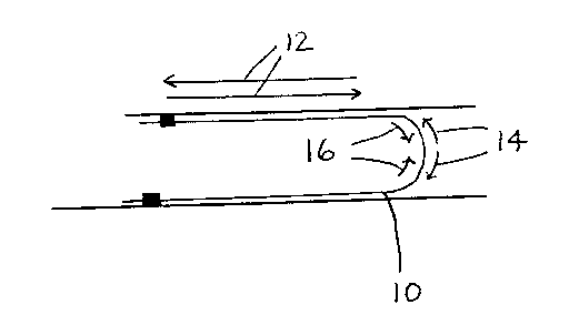
copper foil of the flexible circuit. Referring to Figure 1, flexible circuit
10 is moved
back and forth as indicated by arrows 12. This action mimics the motion of a
disk
drive. Arrows 14 represent tensile forces on the flexible circuit 10 (and
particularly
the copper foil, not shown, thereinl. Arrows 16 represent compressive forces
on
the flexible circuit 1 O land particularly the copper foil, not shown,
therein). As the
flexible circuit 10 is moved back and forth along arrow 12, the tensile forces
and
2
CA 02287707 1999-10-26
GOUFP0530US
the compressive forces move back and forth thereon. The constantly repeated
stress imposed by the tensile forces and the compressive forces leads to roll
fatigue
of the copper foil within flexible circuit 10. Flex fatigue is characterized
by holding
the flexible circuit at two points and applying force normal to the flexible
circuit to
a point about half way between the two holding points followed by applying
another force normal to the flexible circuit in the opposite (180°)
direction. Fold
fatigue is characterized by initially holding the flexible circuit with a
135° bend and
then folding the flexible circuit to have a 0°-2° bend and then
unbending back to
135°. This action mimics the motion of a printer hinge.
The three primary types of fatigue (roll fatigue, flex fatigue, and fold
fatigue)
are generally caused by high cycle, low strain fatigue. Another type of
fatigue is
low cycle, high strain fatigue. It is difficult to provide a flexible circuit
having
resistance to both high cycle, low strain fatigue and low cycle, high strain
fatigue.
Referring to f=igures 2A and 2B, illustrations of microscopic cracks, some of
which extend the thickness or the width of the copper foil and some of which
do
not, are shown. The illustrations are based on photographs taken at a
magnification of 1600X of copper foil having a thickness of about 18 ~cm.
In one embodiment, the present invention relates to a flexible laminate,
comprising a first flexible polymeric film; a copper layer having a
microcracking
prevention layer on at least one side the microcracking prevention layer
sufficient to
prevent microcracks in a copper layer having a thickness of up to about 18 ~m
during at least 50,000,000 bending cycles and/or a copper layer having a
thickness
of up to about 35 ,um during at least 20,000,000 bending cycles of the
flexible
laminate; and a second flexible polymeric film.
3
CA 02287707 1999-10-26
GOUFP0530US
In another embodiment, the present invention relates to a process for making
a flexible laminate, comprising providing a copper layer; treating the copper
layer to
prevent microcracking; affixing a first side of the copper layer to a first
flexible
polymeric film; patterning the copper layer; and affixing a second flexible
polymeric
film to a second side of the copper layer.
In yet another embodiment, the present invention relates to a method of
preventing microcracking in a copper layer having a thickness of up to about
18 ~cm
during at least 50,000,000 bending cycles of a flexible circuit comprising a
first
flexible polymeric film, the copper layer, and a second flexible polymeric
film, the
flexible circuit optionally further comprising an adhesive between at least
one of the
copper layer and the first flexible polymeric film and the copper layer and
the
second flexible polymeric film, comprising treating at least one side of the
copper
layer with a cathodic treatment in an acidic copper sulfate bath, an oxidizing
treatment, a chromium treatment, a catholic treatment in an acid bath, a tie
coat
treatment and a silane treatment.
As a result of the present invention, a flexible circuit having improved
electrical properties is provided. The flexible circuit having improved
electrical
properties exhibits improved resistance to mechanical fatigue and thus
improved
resistance to damage of the copper foil layer, thereby improving the
electrical
properties. The improved resistance to mechanical fatigue is attributable to
the
enhanced resistance to microcracking of the copper foil layer.
Also a result of the present invention, a flexible circuit having improved
flex
to install properties is provided. In this connection, the present invention
provides a
flexible circuit having resistance to both high cycle, low strain fatigue and
low
cycle, high strain fatigue.
4
CA 02287707 1999-10-26
GOUFP0530US
Rripf pescr;,~tion of the Drawing
Figure 1 is a schematic illustration of the bending and corresponding forces
associated with a flexible circuit.
Figures 2A and 2B are illustrations of microcracking in a copper layer after
numerous bending cycles.
In one embodiment, the present invention relates to various treatments for
the copper layer of a flexible circuit in order to prevent, minimize, and/or
delay the
propagation of microcracks due to the local imposition of energy from repeated
bending and unbending cycles. In another embodiment, the present invention
relates to flexible circuits containing a copper layer treated to prevent,
minimize,
and/or delay the generation and propagation of microcracks therein. White not
wishing to be bound by any theory, it is believed that the various treatments
for the
copper layer of a flexible circuit reduce the energy locally imposed upon the
copper
layer, typically caused by tensile forces and/or compressive forces, by at
least one
of distributing the locally imposed energy over a relatively large area of the
copper
layer and absorbing locally imposed energy thereby reducing energy imposed
upon
the copper layer. By reducing the locally imposed energy, the propagation of
microcracks in copper foil is prevented, minimized, and/or delayed. Locally
imposed
energy is stress or force applied on a relatively small portion of a
substrate,
characterized by a large force per unit area. The locally imposed energy is
reduced
by at least one of redistributing the locally imposed energy over a relatively
large
area of the copper layer (thereby decreasing the force per unit area on the
copper
layer) and absorbing locally imposed energy thereby dissipating energy that
would
have been transferred to the copper layer.
5
CA 02287707 1999-10-26
GOUFP0530US
Flexible circuits in accordance with the present invention contain a first
flexible polymeric substrate or film, a copper layer having a microcracking
prevention layer and a second flexible polymeric film or cover layer. The
copper
layer contains copper or a copper alloy. Copper alloys contain copper and at
least
one of the aluminum, chromium, zinc, gold, silver, palladium, platinum,
nickel,
cobalt, titanium, scandium and zirconium. Optionally, an adhesive is present
in
between the copper layer and at least~one of the first flexible polymeric film
and the
second flexible polymeric film.
The copper treatments for preventing, minimizing, and/or delaying the
propagation of microcracks include one or more of a cathodic treatment in an
acidic
copper sulfate bath, an oxidizing treatment, a chromium treatment, a zinc-
oxidation
treatment, and a cathodic treatment in an acid bath. In one embodiment, at
least
one of a tie coat treatment and a silane treatment are combined with one or
more
of the cathodic treatment in an acidic copper sulfate bath, the oxidizing
treatment,
the chromium treatment, a zinc-oxidation treatment,. and the cathodic
treatment in
an acid bath. One or both sides of the copper foil may be treated in
accordance
with the invention.
Flexible circuits containing copper foil having a microcracking treatment
layer
in accordance with the present invention undergo substantially more bending
cycles
before microcracking occurs compared with flexible circuits that do not
contain
copper foil having the microcracking treatment layer (that is, they resist
microcracking for a longer period of time). In one embodiment, flexible
circuits
containing copper foil having a microcracking treatment layer in accordance
with
the present invention undergo 25% more bending cycles before microcracking
occurs compared with flexible circuits that do not contain copper foil having
the
microcracking treatment layer. In another embodiment, flexible circuits
containing
copper foil having a microcracking treatment layer in accordance with the
present
6
CA 02287707 1999-10-26
GOUFP0530US
invention undergo 50% more bending cycles before microcracking occurs compared
with flexible circuits that do not contain copper foil having the
microcracking
treatment layer. In yet another embodiment, flexible circuits containing
copper foil
having a microcracking treatment layer in accordance with the present
invention
undergo 100% more bending cycles before microcracking occurs compared with
flexible circuits that do not contain copper foil having the microcracking
treatment
layer. In still yet another embodiment, flexible circuits containing copper
foil having
a microcracking treatment layer in accordance with the present invention
undergo
an order of magnitude more bending cycles before microcracking occurs compared
with flexible circuits that do not contain copper foil having the
microcracking
treatment layer.
In one embodiment, the present invention permits the prevention of
microcracking in a copper layer having a thickness of up to about 18 gum
during at
least 20,000,000 bending cycles of a flexible circuit (roll fatigue). In
another
embodiment, the present invention pemnits the prevention of microcracking in a
copper layer having a thickness of up to about 18 ~m during at least
50,000,000
bending cycles of a flexible circuit (roll fatigue). In yet another
embodiment, the
present invention permits the prevention of microcracking in a copper layer
having a
thickness of up to about 35 ~m during at feast 20,000,000 bending cycles of a
flexible circuit (roll fatigue). In still yet another embodiment, the present
invention
permits the prevention of microcracking in a copper layer having a thickness
of up
to about 35 um during at least 30,000,000 bending cycles of a flexible circuit
(roll
fatigue).
The copper treatment involving a cathodic treatment in an acidic copper
sulfate bath functions to transfer local stress on the copper layer to a
relatively
large area on the copper layer. The acidic copper sulfate bath is typically at
a
temperature from about 5°C to about 50°C, and preferably from
about 10°C to
7
CA 02287707 1999-10-26
GOUFP0530US
about 40°C. The acidic copper sulfate bath is preferably a dilute
acidic copper
sulfate bath. In this connection, the concentration of copper sulfate in the
acidic
copper sulfate bath is from about 0.1 g/I to about 60 g/I. In another
embodiment,
the concentration of copper sulfate is from about 1 g/l to about 30 g/I. In
one
embodiment, the resultant microcracking prevention layer of this embodiment
has a
thickness from about 0.01 ~m to about 30 ~cm. In another embodiment, the
resultant microcracking prevention layer of this embodiment has a thickness
from
about 0.1 ~cm to about 10 ~cm.
i 0 Two flexible laminates are provided, one conventional and one according to
the present invention. The first flexible laminate (conventional) contains a
copper
layer having a thickness of about 18 ~cm, one adhesive layer next to one side
of the
copper foil having a thickness of about 25 ~cm, and two polyimide layers, one
covering the adhesive layer having a thickness of about 25 ~cm, and the other
having a thickness of about 50 ~cm attached directly to the copper layer. The
second flexible laminate (according to the present invention) also contains a
copper
layer having a thickness of about 18 Vim, one adhesive layer next to the one
side of
the copper foil having a thickness of about 25 Vim, and two polyimide layers,
one
covering the adhesive layer having a thickness of about 25 ,um, the other
having a
thickness of about 50 ~cm attached directly to the copper layer, but one side
of the
copper layer is contacted with an acidic copper sulfate bath containing about
50 g/l
of copper sulfate at a temperature of about 30°C for a time sufficient
to form a
microcracking prevention Payer having a thickness of about 1 ~cm.
The flexible laminates are subjected to bending cycles similar to that shown
in Figure 1. At intervals of 5,000,000 cycles, the copper foil is examined
under
magnification of about 1600X to determine the presence and extend of
microcracking. The first flexible laminate displays some microcracking at
8
CA 02287707 1999-10-26
GOUFP0530US
5,000,000 cycles and extensive microcracking (some through the copper foil) at
10,000,000 cycles. The second flexible laminate displays some microcracking at
20,000,000 cycles and extensive microcracking (some through the copper foil)
at
40,000,000 cycles.
The copper treatment involving an oxidizing treatment involves the use of an
oxidant to oxidize the surface of the copper layer of the flexible circuit.
The
oxidizing treatment functions to distribute locally imposed energy over a
relatively
large area of the copper layer and/or absorb locally imposed energy thereby
dissipating energy going to the copper layer.
In one embodiment, the oxidizing treatment involves providing brown oxide
on the copper layer surface. In another embodiment, the oxidizing treatment
involves providing a black oxide layer on the surface of the copper layer of
the
flexible circuit. Brown and black oxides are provided by contacting an oxidant
with
the surface of the copper layer preferably in the presence of an electric
current.
Common oxidants include chlorite, sulfite, hypochlor'rte and hyposulfite.
Typically,
the black oxide layer is obtained after a more thorough oxidation of the
copper foil
compared to the oxidation of the black oxide. Brown or black oxides are
obtained
depending upon at least one of the concentration of the oxidant and the time
in
which the copper foil is in contact with the oxidant. In embodiments where a
brown oxide is desired, the concentration of the oxidant is from about 10 g/i
to
about 100 g/I, and preferably from about 15 g/I to about 30 g/I. In
embodiments
where a black oxide is desired, the concentration of the oxidant is from about
40
g/I to about 150 g/I, and preferably from about 40 gh to about 60 g/l. In
embodiments where a brown oxide is desired, the copper foil is in contact with
an
oxidant solution from about 10 seconds to about 3 minutes, and preferably from
about 30 seconds to about 90 seconds. In embodiments where a black oxide is
desired, the copper foil is in contact with an oxidant solution from about 3
minutes
9
CA 02287707 1999-10-26
GOUFP0530US
to about 10 minutes, and preferably from about 5 minutes to about 7 minutes.
In
these embodiments, the thickness of the brown oxide layer is from about 0.01
~m
to about 1 ~cm and the thickness of the black oxide layer is from about 0.02
~m to
about 2 ~cm. In another embodiment, the thickness of the brown oxide layer is
from about 0.05 ~cm to about 0.2 ~cm and the thickness of the black oxide
layer is
from about 0.07 ~cm to about 0.5 Vim.
Two flexible laminates are provided, one conventional and one according to
the present invention. The first flexible laminate (conventional) is the same
as the
first flexible laminate disclosed in Example 1. The second flexible Laminate
(according to the present invention) is the same as the second flexible
laminate of
Example 1 except that one side of the copper layer is contacted with an
oxidizing
solution containing about 50 g/! of sodium hypochlorite for about 6 minutes ~o
provide a black oxide layer.
The flexible laminates are subjected to bending cycles similar to that shown
in~ Figure 7 . At intervals of 5,000,000 cycles, the copper foil is examined
under
magnification of about 9 600X to determine the presence and extend of
microcracking. The first flexible laminate displays some microcracking at
5,000,000 cycles and extensive microcracking (some through the copper foil) at
10,000,000 cycles. The second flexible laminate displays some microcracking at
20,000,000 cycles and extensive microcracking (some through the copper foil)
at
25,000,000 cycles.
Two flexible laminates are provided, one conventional and one according to
the present invention. The first flexible laminate (conventional) is the same
as the
first flexible laminate disclosed in Example 1. The second flexible laminate
(according to the present invention) is the same as the second flexible
laminate of
CA 02287707 1999-10-26
GOUFP0530US
Example 1 except that one side of the copper layer is contacted with an
oxidizing
solution containing about 20 g/I of sodium hypochlorite for about 60 seconds
to
provide a brown oxide layer.
The flexible laminates are subjected to bending cycles similar to that shown
in Figure 1. At intervals of 5,000,000 cycles, the copper foil is examined
under
magnification of about 1600X to determine the presence and extend of
microcracking. The first flexible laminate displays some microcracking at
5,000,000 cycles and extensive microcracking (some through the copper foil) at
10,000,000 cycles. The second flexible laminate displays some microcracking at
25,000,000 cycles and extensive microcracking (some through the copper foil)
at
30,000,000 cycles.
In another embodiment, the brown oxide is provided by contacting the
copper foil with a solution of an oxidizer and a hyd~ oxide compound. The
copper
foil is contacted with this solution via any conventional means including
dipping,
spraying, wiping, immersing and the like, although immersing the copper foil
in this
solution is preferred. Application of an electrical current is got required.
In this embodiment, the temperature of the solution is from about 10°C
to
about 90°C, and more preferably from about 40°C to about
80°C. In one
embodiment, the copper foil is placed in the oxidizer solution from about 2 to
about
20 seconds, and more preferably from about 5 to about 10 seconds.
The oxidizer is a chemical compound capable of oxidizing the surface of the
copper foil. Oxidizers include ammonium, alkali metal and alkaline earth metal
oxidizers. The term "ammonium as used herein includes both ammonium ions
(NH4+) and organic ammonium ions such as tetramethylammonium,
tetraethylammonium, tetrapropylammonium and tetrabutylammonium ions. Alkali
metals include lithium, sodium, potassium and rubidium, sodium and potassium
being preferred. Alkaline earth metals include beryllium, magnesium, calcium,
11
CA 02287707 1999-10-26
GOUFP0530US
strontium and barium, magnesium and calcium being preferred. Examples of
oxidizers include ammonium, alkali metal and alkaline earth metal, chlorites,
hypochlorites, nitrates, nitrites, percarbonates, perborates, perchlorates,
periodates
and persulfates.
Specific examples include ammonium nitrate, ammonium perchlorate,
ammonium persulfate, tetramethylammonium nitrate, tetraethylammonium nitrate,
sodium chlorite, sodium hypochlorite, sodium nitrate, sodium nitrite, sodium
perborate, sodium percarbonate, sodium perchlorate, sodium periodate, sodium
persulfate, potassium nitrate, potassium nitrite, potassium perborate,
potassium
perchlorate, potassium periodate, potassium persulfate, rubidium nitrate,
rubidium
perchlorate, magnesium nitrate, magnesium perchlorate, calcium hypochlorite,
calcium nitrate, calcium perchlorate, strontium nitrate, and strontium
perchlorate.
Preferred oxidizers include sodium hypochlorite, sodium chlorite and sodium
persulfate. The oxidizer is present in the solution an amount ranging from
about 20
to about 180 g/I, and preferably from about 30 to about 170 g/1, and more
preferably from about 50 to about 160 g/I.
The hydroxide compound is any compound capable of providing hydroxide
ions in solution. Examples of hydroxide compounds include ammonium, alkali
metal
and alkaline earth metal hydroxides. Specific examples of hydroxide compounds
include ammonium hydroxide, tetramethylammonium hydroxide,
tetraethylammonium hydroxide, sodium hydroxide, potassium hydroxide,
magnesium hydroxide, and calcium hydroxide. The hydroxide compound is present
in the solution in an amount less than about 5 g/I, preferably Less than about
3 g/I,
more preferably less than about 2 g/I, and more preferably less than about 1.5
g/I.
In this embodiment, the oxidizer solution contains a suitable solvent such as
water, polar organic liquids such as alcohols and glycols, and/or mixtures
thereof.
12
CA 02287707 1999-10-26
GOUFP0530US
Aqueous solutions are preferred. Various additives may also be contained in
the
oxidizer solution.
In one embodiment, the ratio in g/I of the oxidizer to the hydroxide compound
is at least about 20:1. In another embodiment, the ratio of the oxidizer to
the
hydroxide compound is at least about 30:1. In a preferred embodiment, the
ratio of
the oxidizer to the hydroxide compound is at least about 50:1. In a most
preferred
embodiment, the ratio of the oxidizer to the hydroxide compound is at least
about
60:1. In these embodiments, the ratio is necessary for proper interaction
between
the oxidizing solution and the metal foil.
In this embodiment, the oxide layer has a thickness from about 50 to about
250 A, but less than about 250 ~. In another embodiment, the thickness of the
resultant oxide layer on the copper foil is from about 75 to about 200 R, but
less
than about 200 ~. In yet another embodiment, the thickness of the resultant
oxide
layer on the copper foil is from about 100 to about 175 A, but less than about
175
A.
The solution containing the oxidizer leads to the formation of an oxide layer
on the copper foil. As a result of the relatively low amount of hydroxide
compound
present in the solution, the quality of the oxide layer for dissipating
tensile stress
and compressive stress is increased without electrolytically treating the
copper foil.
Two flexible laminates are provided, one conventional and one according to
the present invention. The first flexible laminate (conventional) is the same
as the
first flexible laminate disclosed in Example 1. The second flexible laminate
(according to the present invention) is the same as the second flexible
laminate of
Example 1 except that one side of the copper layer is contacted with an
oxidizing
solution containing about 90 g/I of sodium hypochlorite and about 2 g/I sodium
hydroxide at about 50°C for about 7 seconds to provide a brown oxide
layer.
13
CA 02287707 1999-10-26
GOUFP0530US
The flexible laminates are subjected to bending cycles similar to that shown
in Figure 1. At intervals of 5,000,000 cycles, the copper foil is examined
under
magnification of about 1600X to determine the presence and extend of
microcracking. The first flexible laminate displays some microcracking at
5,000,000 cycles and extensive microcracking (some through the copper foil) at
10,000,000 cycles. The second flexible laminate displays some microcracking at
25,000,000 cycles and extensive microcracking (some through the copper foil)
at
30,000,000 cycles.
In yet another embodiment, plasma may be applied to the copper foil surface
for an effective period of time and at a sufficient level of intensity to
chemically
modify the surface, and thereby enhancing resistance to microcracking. The
plasma used to treat the film surface is comprised of ionized oxygen that is
produced ~~sing a non-metallizing cathode. The term "non-metallizing cathode"
refers to cathodes that do not deposit significant levels of metal or metal
oxide on
the surface of the copper layer. The term "significant levels" refers to
levels of no
more than about 0.1 atomic percent as measured by x-ray photoelectron
spectroscopy. The non-metallizing cathodes include non-metallic cathodes such
as
carbon cathodes. In one embodiment, certain metal cathodes such as cathodes
constructed of AI, Ti, V, and mixtures of two or more thereof can be used.
Carbon
cathodes are preferred. Direct current or alternating current can be used,
with
direct current being preferred. The plasma gas can be oxygen, air or gaseous
mixtures containing oxygen at a concentration of up to about 100%, and in one
embodiment about 15% to about 100%, and one or more second gases (e.g., N2,
Ar, Kr, NH3, NZO, CF4, COZ or one or more noble gases). In one embodiment, the
plasma gas is oxygen or air. The pressure in the plasma chamber is typically
in the
range of about 10 to about 500 mTorr, and in one embodiment about 20 mTorr to
about 200 mTorr, and in one embodiment about 30 mTorr to about 150 mTorr, and
14
CA 02287707 1999-10-26
GOUFP0530US
in one embodiment about 40 to about 100 mTorr. The discharge power density is
in the range of about 0.1 to about 8 W/cm2, and in one embodiment about 0.17
to
about 6.2 W/cm2, and in one embodiment about 0.34 to about 2.41 W/cm2. The
total energy input into the surface is in the range of about 0.02 to about 150
J/cm2, and in one embodiment about 0.05 to about 113 J/cm2, and in one
embodiment about 0.4 to about 11.3 J/cm2.
The copper layer can be subjected to one or more than one plasma treatment
steps. In this embodiment, the oxidizing treatment involves contacting oxygen
plasma with the surface of the copper layer of the flexible circuit to form an
oxide
layer having a thickness from about 0.01 ~cm to about 5 Vim, and preferably
from
about 0.1 ~m to about 1 ~cm.
Two flexible laminates are provided, one conventional and one according to
the present invention. The first flexible laminate (conventional) is the same
as the
first flexible laminate disclosed in Example 1. The second flexible laminate
(according to the present invention) is the same as the second flexible
laminate of
Example 1 except that one side of the copper layer is contacted with an
oxidizing
plasma containing oxygen at 150 mTorr using a discharge power density of about
4
W/cm2.
The flexible laminates are subjected to bending cycles similar to that shown
in -Figure 1. At intervals of 5,000,000 cycles, the copper foil is examined
under
magnification of about 1600X to determine the presence and extend of
microcracking. The first flexible laminate displays some microcracking at
5,000,000 cycles and extensive microcracking (some through the copper foil) at
10,000,000 cycles. The second flexible laminate displays some microcracking at
30,000,000 cycles and extensive microcracking (some through the copper foil)
at
40,000,000 cycles.
CA 02287707 1999-10-26
GOUFP0530US
In still yet another embodiment, the oxidizing treatment involves a mild
oxidation treatment in a solution of aerated water. The solution contains
water
having a sufficient amount of dissolved oxygen therein to oxidize the surface
of the
copper foil. In this embodiment, the temperature of the aerated water solution
is
from about 2°C to about 50°C. In another embodiment, the
temperature of the
aerated water oxidizer solution is from about 10°C to about
40°C. In yet another
embodiment, the temperature of the aerated water solution is from about
15°C to
about 30°C. In one embodiment, the copper foil is contacted with the
aerated
water solution from about 1 to about 100 seconds. In another embodiment, the
copper foil is contacted with the aerated water solution from about 2 to about
50
seconds. In yet another embodiment, the metal foil is contacted with the
aerated
water solution from about 5 to about 25 seconds.
In a preferred embodiment, the water is deionized water, although tap water
may be used. The water of the aerated water solution contains at least about 7
ppm dissolved oxygen. In a preferred embodiment, the water of the aerated
water
solution contains at least about 7.5 ppm dissolved oxygen. In one embodiment,
the water contains from about 8 ppm to about 20 ppm dissolved oxygen. In
another embodiment, the water contains from about 9 ppm to about 15 ppm.
Water containing the specified levels of dissolved oxygen may be obtained by
acquiring water with relatively high levels of dissolved oxygen or aerating
water
with pure oxygen gas or a gas containing oxygen until the desired dissolved
oxygen
level is reached. Gases containing oxygen include air and mixtures of oxygen
and
one or more of inert and nonreactive gases such as hydrogen, nitrogen, helium,
neon, argon, krypton and xenon. During the inventive process, the aerated
water
solution may be periodically or continually aerated to maintain a desired
minimum
level or range of dissolved oxygen.
16
CA 02287707 1999-10-26
GOUFP0530US
The oxygen level of the aerated water solution may be periodically or
continually measured using any known means to measure dissolved oxygen
content. For example, one apparatus is under the trade designation YSI Model
57
Series Dissolved Oxygen Meter from Yellow Springs Instrument Company. Reagent
methods, based on the Winkler method, may also be employed. Dissolved oxygen
reagent sets, using buret titration methods, digital titrator methods, or drop
count
titration methods, dissolved oxygen reagent AccuVac~ ampuls, and Pocket
ColorimeterTM for dissolved oxygen are available from Hach Company.
In this embodiment, the aerated water solution is optionally metal free; that
is, the aerated water solution is characterized by the absence of added metals
or
metal compounds. Trace amounts of metals or metal compounds in tap water and
deionized water may be tolerated. In another embodiment, the aerated water
solution is free of organic solvents; that is, the aerated water solution is
characterized by the absence of added organic solvents. In yet another
embodiment, small amounts (less than about 296 by weight or less than about
196
by weight) of organic solvents may be present in the tap or deionized water.
The oxide layer formed due to contact of the copper foil with the aerated
water solution is very thin. In another embodiment, the oxide layer has a
thickness
from about 1 to about 25 ~, but less than about 25 A. In another embodiment,
the
thickness of the resultant oxide layer on the copper foil is from about 2 to
about 20
A, but less than about 20 ~1. In another embodiment, the thickness of the
resultant
oxide layer on the copper foil is from about 3 to about 15 I~, but less than
about 15
The aerated water solution containing water and at least 7 ppm dissolved
oxygen leads to the formation of a relatively thin oxide layer on the copper
foil. As
a result of the specific amount of dissolved oxygen present in the solution,
the
17
CA 02287707 1999-10-26
GOUFP0530US
quality of the oxide layer is increased without electrolytically treating the
copper
foil.
Two flexible laminates are provided, one conventional and one according to
the present invention. The first flexible laminate (conventional) is the same
as the
first flexible laminate disclosed in Example 1. The second flexible laminate
(according to the present invention) is the same as the second flexible
laminate of
Example 1 except that one side of the copper layer is contacted with an
oxidizing
solution containing about 12 ppm dissolved oxygen at about 30°C for
about 20
seconds to provide a thin brown oxide layer.
The flexible laminates are subjected to bending cycles similar to that shown
in Figure 1. At intervals of 5,000,000 cycles, the copper foil is examined
under
magnification of about 1600X to determine the presence and extend of
microcracking. The first flexible laminate displays some microcracking at
5,000,000 cycles and extensive microcracking (some through the copper foil) at
10,000,000 cycles. The second flexible laminate displays some microcracking at
25,000,000 cycles and extensive microcracking (some through the copper foil)
at
30,000,000 cycles.
The copper treatment involving a chromium treatment functions to distribute
locally imposed energy over a relatively large area of the copper layer and/or
absorb
locally imposed energy thereby dissipating energy going to the copper layer.
In one
embodiment, the chromium treatment involves contacting the copper layer with a
chromate (Cr03) solution. This may be accomplished by spraying or dipping the
copper layer in a chromate solution. Chromate may be derived from a number of
sources including potassium chromate and magnesium chromate. In one
embodiment, the concentration of chromate in the chromate solution is from
about
0.1 g/I to about 10 g/I. In another embodiment, the concentration of chromate
in
18
CA 02287707 1999-10-26
GOUFP0530US
the chromate solution is from about 1 g/I to about 5 g/I. In one embodiment,
the
copper foil is in contact with the chromate solution from about 1 seconds to
about
100 seconds, and preferably from about 3 seconds to about 10 minutes.
Two flexible laminates are provided, one conventional and one according to
the present invention. The first flexible laminate (conventional) is the same
as the
first flexible laminate disclosed in Example 1. The second flexible laminate
(according to the present invention) is the same as the second flexible
laminate of
Example 1 except that one side of the copper layer is contacted with a
chromate
solution containing about 2 gll of chromate at a temperature of about
25°C for
about 7 seconds.
The flexible laminates are subjected to bending cycles similar to that shown
in Figure 1. At intervals of 5,000,000 cycles, the copper foil is exami~ red
under
magnification of about 1600X to determine the presence and extend of
microcracking. The first flexible laminate displays some microcracking at
5,000,000 cycles and extensive microcracking (some through the copper foil) at
10,000,000 cycles. The second flexible laminate displays some microcracking at
20,000,000 cycles and extensive microcracking (some through the copper foil)
at
30,000,000 cycles.
In another embodiment, the chromate treatment involves a cathodic
° '
treatment in a chromate solution. In particular, copper foil is placed in a
chromium
containing electrolytic bath. The chromium containing electrolytic bath is an
aqueous solution containing a chromium compound and optionally performance
enhancing additives. A current is applied to the bath so that a cathodic
chrome
layer is electrolytically deposited on the copper foil. The chromium compound
is
any compound capable of depositing a thin layer of cathodic chrome or chromium
onto the copper foil. Examples of chromium compounds include chromium oxide
19
CA 02287707 1999-10-26
GOUFP0530US
such as chromium trioxide, chromium anhydride, chromic acid, hexavalent
chromium compounds, dichromates such as potassium dichromate and sodium
dichromate, and chromates such as potassium chromate, sodium chromate and
magnesium chromate. The chromium compound is present in the chromium
containing electrolytic bath in an amount from about 0.1 to about 5 gll, and
preferably from about 1 to about 3 g/I.
Optional performance enhancing additives include zinc compounds, such as
zinc salts (for example, zinc acetate, zinc chloride, zinc nitrate and zinc
sulfate).
In one embodiment, the temperature of the chrome containing electrolytic
bath during the electrodeposition step is from about 15°C to about
30°C, and
preferably from about 20°C to about 25°C. The pH of the chromium
containing
electrolytic bath depends upon the identity of the particular chromium
compound of
a specific embodiment, and thus is not critical. In one embodiment, the
current
density applied to the chromium containing electrolytic bath is from about 10
to
about 40 ASF. In another embodiment, the current density is from about 15 to
about 35 ASF, and more preferably from about 20 to about 30 ASF. The copper
foil is placed in the chromium containing electrolytic bath for a time
sufficient to
permit the formation of a relatively thin but uniform cathodic chrome Layer
over the
copper foil surface. In one embodiment, the copper foil is placed in the
chromium
containing electrolytic bath from about 2 to about 20 seconds, and more
preferably
from about 5 to about 10 seconds.
In one embodiment, the thickness of the resultant cathodic chrome layer is
from about 25 to about 125 ~. In a preferred embodiment, the thickness of the
resultant cathodic chrome layer is from about 50 to about 100 ~. The thickness
of
the cathodic chrome layer is substantially uniform over the entire surface of
the
copper foil and follows any contours on the surface of the copper foil.
CA 02287707 1999-10-26
GOUFP0530US
Two flexible laminates are provided, one conventional and one according to
the present invention. The first flexible laminate (conventional) is the same
as the
first flexible laminate disclosed in Example 1. The second flexible laminate
(according to the present invention) is the same as the second flexible
laminate of
Example 1 except that one side of the copper layer is contacted with a
chromium
containing electrolytic bath containing about 3 g/I chromium at a temperature
of
about 25°C for about 10 seconds under 25 ASF.
The flexible laminates are subjected to bending cycles similar to that shown
in Figure 1. At intervals of 5,000,000 cycles, the copper foil is examined
under
magnification of about 1600X to determine the presence and extend of
microcracking. The first flexible laminate displays some microcracking at
5,000,000 cycles and extensive microcracking (some through the copper foil) at
10,000,000 cycles. The second flexible laminate displays same microcracking at
30,000,000 cycles and extensive microcracking (some through the copper foil)
at
40,000,000 cycles.
In yet another embodiment, the chromium treatment may involve a cathodic
treatment in an acidic chromate solution containing zinc and a hydrogen
inhibitor
such as phosphorous. The chromium treatment applies a metal layer to the
copper
foil by contacting the copper foil with an electrolyte solution comprising
zinc ions,
chromium ions and at least one hydrogen inhibitor. The source of zinc ions for
the
electrolyte solution can be any zinc salt. Examples include ZnS04, ZnC03,
ZnCr04,
zinc polyphosphate, zinc sulfamate, etc. The source of chromium ions for the
electrolyte solution can be any hexavalent chromium salt or compound, examples
include ZnCr04, Cr03, chromium trioxide, chromium anhydride, hexavalent
chromium compounds, dichromates such as potassium dichrori~ate and sodium
dichromate, and chromates such as potassium chromate, sodium chromate and
magnesium chromate.
21
CA 02287707 1999-10-26
GOUFP0530US
The hydrogen inhibitor can be any additive for the electrolyte solution in
this
embodiment that inhibits hydrogen evolution during the application process.
These
include the following ions: p+3, W+s~ V+s~ As+s~ As+s~ Pb+2~ Pb+a~ Hg+~~ Hg+2~
Cd+2 or quaternary ammonium ions. P+3, W+s and V+5 are particularly preferred,
and P+3 is especially preferred. Sources for these ions include H3P03, Na2W04,
Na3V04 HAs03, Pb(N03)2, Pb~N03)4, Hg2S04, HgS04, CdS04, and the like.
The quaternary ammonium ions can be any compound or cation derived from
the formula
Ra
Rs _ N + R, X_
_
R2
wherein R', R2, R3 and R4 are independently hydrocarbon groups of 1 to about
16
carbon atoms, and in one embodiment 1 to about 8 carbon atoms, and in one
embodiment about 4 carbon atoms, and X- is an anion such as CI', OH-,
carbonate, bicarbonate, nitrate or other such anion, which acts as a
counterion to
the quaternary ammonium. A particularly preferred quaternary ion includes
tetrabutyl ammonium ions derived from tetrabutyl ammonium hydroxide.
The concentration of zinc ions in the electrolyte solution is generally in the
range from about 0.1 to about 2 g/I, and in one embodiment about 0.3 to about
1
g/I, and in another embodiment about 0.4 to about 0.5 g/l. The concentration
of
chromium ions in the electrolyte solution is generally in the range from about
0.3 to
about 5 g/I, and in one embodiment about 0.5 to about 3 g/l, and in another
embodiment about 0.5 to about 1.0 g/I. The concentration of hydrogen inhibitor
ions is generally in the range from about 5 ppm to about 1000 ppm, and in one
embodiment about 100 ppm to about 500 ppm. In one embodiment, the
22
CA 02287707 1999-10-26
GOUFP0530US
concentration of P+3 ions in the electrolyte solution is in the range of about
100
ppm to about 500 ppm, and in one embodiment about 150 ppm to about 250 ppm.
The electrolyte solution can include other additives such as Na2S04 at
concentrations in the range from about 1 to about 50 g/I, and in one
embodiment
about 10 to about 20 g/I. The pH of the electrolyte solution is generally in
the
range from about 3 to about 6, and in one embodiment about 4 to about 5. The
current density employed is generally in the range from about 1 to about 100
amps/ft2, and in one embodiment about 25 to about 50 amps/ft2, and in another
embodiment about 30 amps/ft2.
The temperature of the electrolyte solution is generally in the range from
about 20°C to about 100°C, and in one embodiment about
25°C to about 45°C.
The plating time employed is generally in the range from about 1 to about 30
seconds, and in one embo~~ment about 5 to about 20 seconds. In one
embodiment, the total treatment time is from about 1 to about 10 seconds, and
in
another embodiment, the total treatment time is from about 2 to about 8
seconds.
In one embodiment, the mole ratio of chromium ions to zinc ions in the
electrolyte solution is in the range from about 0.2 to about 10, and in one
embodiment about 7 to about 5. The mole ratio of zinc ions to hydrogen
inhibitor
ions in the electrolyte solution is, in one embodiment, in the range from
about 0.4
to about 10, and in one embodiment about 1 to about 2.
The thickness of the resultant layer that is applied to the copper foil is
generally in the range from about 0.001 to about 0.5 microns, and in one
embodiment about 0.005 to about 0.01 microns.
Two flexible laminates are provided, one conventional arid one according to
the present invention. The first flexible laminate (conventional) is the same
as the
first flexible laminate disclosed in Example 1. The second flexible laminate
23
CA 02287707 1999-10-26
GOUFP0530US
(according to the present invention? is the same as the second flexible
laminate of
Example 1 except that one side of the copper layer is contacted with an acidic
electrolytic bath containing about 0.5 g/I zinc, about 2 g/l chromium and
about 200
ppm phosphorus at a temperature of about 25°C for about 10 seconds
under 30
ASF.
The flexible laminates are subjected to bending cycles similar to that shown
in Figure 1. At intervals of 5,000,000 cycles, the copper foil is examined
under
magnification of about 1600X to determine the presence and extend of
microcracking. The first flexible laminate displays some microcracking at
5,000,000 cycles and extensive microcracking (some through the copper foil) at
10,000,000 cycles. The second flexible laminate displays some microcracking at
35,000,000 cycles and extensive microcracking (some through the copper foil)
at
45,000,000 cycles.
The copper treatment may involve a zinc-oxidation treatment. The zinc-
oxidation treatment forms a zinc oxide that functions to distribute locally
imposed
energy over a relatively large area of the copper layer and/or absorb locally
imposed
energy thereby dissipating energy going to the copper layer.
In one embodiment, a zinc metal layer is deposited on the copper foil,
followed by oxidation into a zinc oxide layer. The zinc metal layer has a
thickness
of about 2 ~ to about 60 ~, and in another embodiment about 2 r~ to about 50
~,
and in yet another embodiment about 5 ~ to about 40 ~, and in stilt yet
another
embodiment about 1 O /~ to about 35 ~1.
In one embodiment, the layer of zinc metal is applied to the copper foil
surface using vapor deposition. Any of the vapor deposition techniques known
in
the art can be used. These include physical vapor deposition (FVD) and
chemical
vapor deposition (CVD) techniques. Physical vapor deposition includes thermal
evaporation, electron beam deposition, inductive and/or resistive deposition,
ion
24
CA 02287707 1999-10-26
GOUFP0530US
plating, sputtering, plasma-activated evaporation, reactive evaporation, and
activated reactive evaporation. Physical vapor deposition also has been
referred to
in the literature as vacuum metallization and evaporative coating. In thermal
evaporation deposition procedures, the zinc metal to be applied to the copper
foil is
heated in a high vacuum le.g., 10-2 to about 10'6 tort) whereupon the zinc
metal
evaporates or sublimates and travels to the copper foil surface. In sputtering
processes, energetic inert ions created in a plasma discharge impact a target
and
cause the ejection of zinc metal through momentum exchange. Physical vapor
deposition essentially involves the transfer of the zinc metal and the
formation of a
zinc layer on the copper foil by physical means alone in contrast to chemical
vapor
deposition in which the zinc metal transfer is effected by chemical reactions
induced by temperature or concentration gradients between the substrate and
the
surrounding gaseous atmosphere. The principals of vapor deposition and
procedures useful in vapor depositing various metals is described in y_al~
Deposition. edited by C.F. Powell et al., John Wiley & Sons, Inc., New York,
1966,
which is incorporated herein by reference.
Chemical vapor deposition usually is accomplished by vaporizing a zinc
halide and decomposing or reacting the vapors at the foil surface to yield a
non-
volatile zinc metal on the surface of the foil as a coating. The chemical
reactions of
vapor deposition can be effected by thermal deposition or pyrolysis, hydrogen
reduction, reduction with metal vapors, reaction with the copper foil,
chemical
transport reactions, etc. These procedures are described in detail in Chapter
9 of
yaaor DeRosition, C.F. Powell, et al., J. Wiley & Sons, Inc., New York, 1966.
This chapter is incorporated herein by reference for its description of the
CVD
processes.
The zinc metal layer is oxidized by applying a hexavalent chromium oxide
layer to its surface using known electroplating techniques. During this
process the
CA 02287707 1999-10-26
GOUFP0530US
hexavalent chromium oxide is converted or reduced to trivalent chromium oxide.
0
The resulting trivalent chromium oxide layer has a thickness of about 20 A to
about
100 ~, and in one embodiment about 20 ~ to about 60 ~, and in another
embodiment about 30 ~ to about 40 ~. The source of hexavalent chromium oxide
can be chromium trioxide (Cr03), a chromyl (Cr02++) compound such as chromyl
amide (Cr02(NHZ)2) or chromylchloride (Cr02C12), a chromate (Cr04') compound
such as Na2Cr204 or KZCr204, or a dichromate (Cr20~') compound such as
Na2Cr20~
or K2Cr20~, The concentration of hexavalent chromium oxide compounds in the
electrolyte solution is generally in the range of about 1 to about 5 g/I, and
in one
embodiment about 2 to about 4 g/I, and in another embodiment about 3 g/I. The
electrolyte solution can include other conventional additives such as Na2S04
at
concentrations in the range of about up to about 15 g/I, and in one embodiment
1
to about 15 g/I. The pH used in the electrolyte solution is generally in the
range of
about 1.5 to about 9. The current density is generally in the range of about 2
to
about 20 amps/ft2, and in one embodiment about 10 to about 20 amps/ft2. The
temperature of the electrolyte solution is generally in the range of about 20
to
about 50 °C, and in one embodiment about 35 to about 40 °C. The
plating time
that is used is generally in the range of about 2 to about 15 seconds, and in
one
embodiment about 5 to about i 2 seconds.
The layer of zinc oxide has a thickness of about 3 ~ to about 80 ~1, and in
one embodiment about 5 ~1 to about 60 ~, and in another embodiment about 10
to about 50 ~, and in yet another embodiment about 15 ~ to about 40 ~, and in
still yet another embodiment about 20 ~ to about 35 ~1.
Two flexible laminates are provided, one conventional arid one according to
the present invention. The first flexible laminate (conventional) is the same
as the
first flexible laminate disclosed in Example i . The second flexible laminate
26
CA 02287707 1999-10-26
GOUFP0530US
(according to the present invention) is the same as the second flexible
laminate of
Example 1 except that one side of the copper layer is contacted by vapor
deposition
with zinc to a depth of about 60 ~. Then, the zinc treated copper foil is
contacted
with 3 g/I hexavalent chromium oxide electrolyte solution under 15 ASF at
about
40°C for about 10 seconds.
The flexible laminates are subjected to bending cycles similar to that shown
in Figure 1. At intervals of 5,000,000 cycles, the copper foil is examined
under
magnification of about 1600X to determine the presence and extend of
microcracking. The first flexible laminate displays some microcracking at
5,000,000 cycles and extensive microcracking (some through the copper foil) at
10,000,000 cycles. The second flexible laminate displays some microcracking at
40,000,000 cycles and extensive microcracking (some through the copper foil)
at
55,000,000 cycles.
The copper treatment may involve the deposition of a tie coat in combination
with one of the preceding copper treatments. The tie coat functions to
distribute
locally imposed energy over a relatively large area of the copper layer and/or
absorb
locally imposed energy thereby dissipating energy going to the copper layer.
The
deposition of a tie coat generally involves a metal deposition step.
In one embodiment, the tie coat deposition involves depositing a chrome tie
coat. In another embodiment, the tie coat treatment involves depositing a
nickel tie
coat. The chrome tie coat is comprised of chromium or a chromium-based alloy.
The alloying metal is selected from Cu, Ni, Fe, V, Ti, AI, Si, Pd, Ta, W, Zn,
In, Sn,
Mn, Co and mixtures of two or more thereof. Preferred alloying metals include
Cu,
Fe, V, Ti and Ni. The chromium tie coat layer has a thickness in the range
from
about 30 ~ to about 500 ~, and in one embodiment about 50 i~ to about 300 ~1.
27
CA 02287707 1999-10-26
GOUFP0530US
The chrome tie coat layer may optionally have a copper seed coat layer
adhered to it. The copper seed coat layer has a thickness from about 200 ~ to
about 20000 ~1, and in one embodiment from about 1200 A to about 5000 A.
The nickel tie coat layer is comprised of nickel or a nickel-based alloy. The
alloying metal is selected from Cu, Cr, Fe, V, Ti, AI, Si, Pd, Ta, W, Zn, In,
Sn, Mn,
Co and mixtures of two or more thereof. Preferred alloying metals include Cu,
Fe,
.
V, Ti and Cr. The nickel tie coat layer has a thickness in the range from
about 30 A
to about 500 ~, and in one embodiment about 50 R to about 300 h.
The nickel tie coat layer may optionally have a copper seed coat layer
adhered to it. The copper seed coat layer has a thickness from about 200 h to
about 20000 ~, and in one embodiment from about 1200 A to about 5000 ~.
The tie coat can be formed or deposited using any of the vapor deposition
techniques known to those skilled in the art, and such techniques include
physical
vapor deposition (PVD) and chemical vapor deposition (CVD). In thermal
evaporation deposition procedures, the metallic material for deposition is
heated in
a high vacuum (e.g., a base pressure of less than about 1 mTorr, and in one
embodiment a base pressure of about 0.001 mTorr) whereupon the metallic
material evaporates or sublimates and travels to the substrate. Chemical vapor
deposition usually is accomplished by vaporizing a metallic halide and
decomposing
or reacting the vapors at the substrate surface to yield the non-volatile
metal on the
surface of the substrate as a coating.
Sputtering is a useful vapor deposition technique for depositing a tie coat.
This technique involves a material transport phenomenon caused by energetic
atoms or ions striking a cathode target, causing the material making up the
cathode
target to be transferred to a vapor state through a momentum transfer
mechanism,
and subsequently to a different surface. The substrate to be coated is placed
adjacent to a cathode. The cathode target is made of the substance which forms
28
CA 02287707 1999-10-26
GOUFP0530US
the coating. The cathode is subjected to a high negative voltage and is placed
in an
inert gas atmosphere at low pressure. Under the influence of the high voltage,
atmospheric ions are accelerated against the surface of the cathode target
wherein
the momentum of the ions is transferred to atoms on the surface of the cathode
target, ejecting the atoms from the surface of the cathode target and causing
them
to contact and adhere to the adjacent substrate. The inert gases that are
useful
include helium, neon, argon, krypton, xenon, and the like.
The metal for deposition is at least one of Cr, a Cr based alloy, Ni and a Ni
based alloy. Useful alloying metals include Cu, Cr, Fe, V, Ti, AI, Ni, Si, Pd,
Ta, W,
Z, In, Sn, Mn, Co, and combinations of two or more thereof. Preferred alloying
metals include Cu, Fe, Cr, Ni and V. Commercially available Ni alloys that are
particularly useful include Monel (about 6796 Ni, 30°6 Cu), Inconel
about (7696 Ni,
1696 Cr, 896 Fe), Nickel "A' (about 99.496 Ni + Co), Nickel ~D° (about
9596 Ni,
4.596 Mn), Duranickel (about 9496 Ni, 4.596 AI), Cast Nickel (about 97% Ni,
1.5%
Si), "K° Monel (about 6696 Ni, 2996 Cu, 396 AI), Monel (cast) (about
6396 Ni, 30°i6
Cu, 1.596 Si), "H° Monel (cast) (about 6396 Ni, 3096 Cu, 396 Si), "S"
Monel (cast)
(about 63% Ni, 3096 Cu, 496 Si), Inconel (cast) (about 7296 Ni, 1696 Cr, 896
Fe,
2% Si), Ni-o-nel (about 42°6 Ni, 3096 Fe, 2296 Cr, 396 Mo, 2°6
Cu, 1 % Ti),
Hastelloy Alloy B (about 6296 Ni, 2896 Mo, 596 Fe), Hastelloy Alloy C (about
54%
Ni, 17°ib Mo, 15°6 Cr, 596 Fe, 496 W), Hastelloy Altoy D (about
8596 Ni, 10% Si,
3% Cu), HasteHoy Alloy F (about 4796 Ni, 2296 Cr, 796 Mo, 17% Fe), Hastelloy
Atloy N (about 709b Ni, 1796 Mo, 796 Cr, 596 Fe), Hastelloy Alloy W (about 62%
Ni, 24.5% Mo, 5% Cr, 5.5% Fe), Hastelloy Alloy X (about 47% Ni, 22% Cr, 9%
Mo, 18% Fe), Illium B (about 5096 Ni, 28% Cr, 8.59'o Mo, 5.5% Cu), Illium G
(about 56% Ni, 22.5% Cr, 6.596 Mo, 6.5% Cu), Illium R (about 68% Ni, 21 % Cr,
5% Mo, 3% Cu), Illium 98 (about 559b Ni, 28% Cr, 8.5% Mo, 5.5% Cu), (about
80% Ni, 20% Crl, (about 60% Ni, 24% Fe, 16% Cr); (about 35% Ni, 45% Fe,
29
CA 02287707 1999-10-26
GOUFP0530US
20% Cr), (about 45% Ni, 55% Cu), and the like. The pressure is in the range of
about 1.5 to about 15 mTorr, and in one embodiment about 2.5 to about 1 O
mTorr.
For depositing the optional copper seed layer, the pressure is in the range of
about 1.5 to about 15 mTorr, and in one embodiment about 2.5 to about 10
mTorr. The thickness of the copper seed coat layer that is deposited is from
about
200 ~ to about 20000 A, and in one embodiment about 1200 ~ to about 5000 ~.
Two flexible laminates are provided, one conventional and one according to
the present invention. The first flexible laminate (conventional) is the same
as the
first flexible laminate disclosed in Example 1. The second flexible laminate
(according to the present invention) is the same as the second flexible
laminate of
Example 1 except that, in addition to the acidic copper sulfate treatment, a
copper
seed layer having a thickness of about 2000 A is deposited via PVD one side of
the
copper layer under 8 mTorr of pressure. Next, a chromium layer having a
thickness
of about 250 A is deposited via PVD over the copper seed layer under 8 mTorr
of
pressure.
The flexible laminates are subjected to bending cycles similar to that shown
in Figure 1. At intervals of 5,000,000 cycles, the copper foil is examined
under
magnification of about 1600X to determine the presence and extend of
microcracking. The first flexible laminate displays some microcracking at
5,000,000 cycles and extensive microcracking (some through the copper foil) at
10,000,000 cycles. The second flexible laminate displays some microcracking at
45,000,000 cycles and extensive microcracking (some through the copper foil)
at
55,000,000 cycles.
CA 02287707 1999-10-26
GOUFP0530US
Two flexible laminates are provided, one conventional and one according to
the present invention. The first flexible laminate (conventional) is the same
as the
first flexible laminate disclosed in Example 1. The second flexible laminate
(according to the present invention) is the same as the second flexible
laminate of
Example 1 except that, in addition to the acidic copper sulfate treatment, a
copper
seed layer having a thickness of about 2000 l~ is deposited via PVD one side
of the
copper layer under 8 mTorr of pressure. Next, a nickel alloy layer having a
thickness of about 250 ~ is deposited via PVD over the copper seed layer under
8
mTorr of pressure using Hastelloy Alloy D as a metal source.
i 0 The flexible laminates are subjected to bending cycles similar to that
shown
in Figure 1. At intervals of 5,000,000 cycles, the copper foil is examined
under
magnification of about 1600X to determine the presence and extend of
microcracking. The first flexible laminate displays some microcrac~mg at
5,000,000 cycles and extensive microcracking (some through the copper foil) at
10,000,000 cycles. The second flexible laminate displays some microoracking at
50,000,000 cycles and extensive microcracking (some through the copper foil)
at
60,000,000 cycles.
The copper treatment involving a silane treatment involves depositing at least
one silane compound on the copper layer of the flexible circuit in combination
with
one of the preceding copper treatments, except for the tie coat treatment. The
copper treatment involving the silane treatment functions to absorb locally
imposed
energy thereby dissipating energy that may be transferred to the copper layer.
tn one embodiment, the silane treatment involves depositing one silane
compound on an otherwise untreated copper layer. The silane treatment is
performed by applying one of the following silane coupling agents to the
copper
foil. The silane coupling agent can be represented by the formula
31
CA 02287707 1999-10-26
GOUFP0530US
RQ_"SiX"
wherein R is a functionally substituted hydrocarbon group, the functional
substituent of said functionally substituted hydrocarbon group being amino,
hydroxy, halo, mercapto, alkoxy, acyl, or epoxy; X is a hydrolyzable group,
such as
alkoxy (e.g., methoxy, ethoxy, etc.), hydroxy group, or halogen (e.g.,
chlorine); and
n is 1, 2 or 3, and preferably n is 3. The silane coupling agents represented
by the
above formula include halosilanes, aminoalkoxysilanes, aminophenylsilanes,
phenyl-
silanes, heterocyclic silanes, N-heterocyclic silanes, acrylic silanes,
mercapto
silanes, and mixture of two or more thereof.
The silane coupling agent can be represented by the formula
O ORs
I\
R'-C-C-R'-O-R6-Si-O R'
R2R OR$
wherein: R', R2 and R3 are independently hydrogen or hydrocarbon groups; R4
and
RS are independently alkylene or alkylidene groups; and Rs, R' and R8 are
indepen-
dently hydrocarbon groups. The hydrocarbon groups preferably contain 1 to
about
10 carbon atoms, more preferably 1 to about 6 carbon atoms, more preferably 1
to
about 4 carbon atoms. These hydrocarbon groups are preferably alkyl. The
alkylene or alkylidene groups R'' and RS preferably contain from 1 to about 10
carbon atoms, more preferably 1 to about 6 carbon atoms, more preferably 1 to
about 4 carbon atoms, more preferably 1 or 2 carbon atoms. The alkylene and
alkylidene groups can be methylene, ethylene, propylene, etc. In one
embodiment,
the silane coupling agent is a compound represented by the formula
32
CA 02287707 1999-10-26
GOUFP0530US
O
/I
CH2CHCH20CH2CH2CHZSi(OCH3ls
The silane coupling agent can be represented by the formula
OR5
R'-C=C-COOR4 Si-OR6
R2 R3 OR'
wherein: R', R2 and R3 are independently hydrogen or hydrocarbon groups; R4 is
an
alkylene or alkyiidene group; and RS, R6 and R' are independently hydrocarbon
groups. The hydrocarbon groups preferably contain 1 to about 10 carbon atoms,
more preferably 1 to about 6 carbon atoms, more preferably 1 to about 4 carbon
atoms. These hydrocarbon groups are preferably alkyl (e.g., methyl, ethyl,
propyl,
etc.y. The afkylene and alkylidene groups preferably contain from 1 to about
10
carbon atoms, more preferably 1 to about 6 carbon atoms, more preferably 1 to
about 4 carbon atoms. The alkylene groups include methylene, ethylene,
propylene, etc. In one embodiment, the silane coupling agent is a compound
represented by the formula
CH3
CH2=C-COOCH2CHZCH2Si(OCH3)s
The silane coupling agent can be represented by the formula
33
CA 02287707 1999-10-26
GOUFP0530US
OR4
R'-N-R3-Si-O R5
1 I
R2 OR6
wherein: R' and R2 are independently hydrogen or hydrocarbon groups; R3 is an
alkylene or alkylidene group; and R4, Rs and R6 are independently hydrocarbon
groups. The hydrocarbon groups preferably contain 1 to about 10 carbon atoms,
more preferably 1 to about 6 carbon atoms, more preferably 1 to about 4 carbon
atoms. These hydrocarbon groups are preferably alkyl (e.g., methyl, ethyl,
propyl,
etc.). The alkylene and alkylidene groups preferably contain from 1 to about
10
carbon atoms, more preferably 1 to about 6 carbon atoms, more preferably 1 to
about 4 carbon atoms. The alkyiene groups include methylene, ethylene,
propylene, etc. In one embodiment this compound is represented by the formula
H2NCHZCH2CH2Si(OC2Hb)s
The silane coupling agent can be represented by the formula
ORg
1
R'-N-R3-N-R5-Si-O R'
R2 R4 OR8
wherein: R', R2 and R4 are independently hydrogen or hydrocarbon groups; R3
and
Rb are independently alkylene or alkylidene groups; and Rs, R' and R8 are
indepen-
dentiy hydrocarbon groups. The hydrocarbon groups preferably contain 1 to
about
10 carbon atoms, more preferably 1 to about 6 carbon atoms, more preferably 1
to
about 4 carbon atoms. These hydrocarbon groups are preferably alkyl (e.g.,
34
CA 02287707 1999-10-26
GOUFP0530US
methyl, ethyl, propyl, etc.). The alkylene and alkylidene groups preferably
contain
from 1 to about 10 carbon atoms, more preferably 1 to about 6 carbon atoms,
more preferably 1 to about 4 carbon atoms. The alkylene groups include
methylene, ethylene, propylene, etc. In one embodiment this compound is
represented by the formula
H2NCH2CH2NHCH2CHZCHZSi(OCH3)s
The silane coupling agent can be represented by the formula
OR3
R'-S-R2 ~i-OR4
O/Re
wherein R' is hydrogen or a hydrocarbon group; R2 is an alkylene or alkylidene
group; and R3, R~ and RS are independently hydrocarbon groups. The hydrocarbon
groups preferably contain 1 to about 10 carbon atoms, more preferably 1 to
about
6 carbon atoms, more preferably 1 to about 4 carbon atoms. These hydrocarbon
groups are preferably alkyl (e.g., methyl, ethyl, propyi, etc.). The alkylene
and
alkylidene groups preferably contain from 1 to about 10 carbon atoms, more
preferably 1 to about 6 carbon atoms, more preferably 1 to about 4 carbon
atoms.
These groups are preferably alkylene (e.g., methylene, ethylene, propylene,
etc.). In
one embodiment, this compound is represented by the formula
HSCH2CH2CH2Si(OCH3)a
The silane coupling agent can be represented by the formula
CA 02287707 1999-10-26
GOUFP0530US
R' R2C = C-Ar-R4-N-R6-N-R8-Si ( O R9) 3'H X
1Ra \Rs R~
wherein: R', R2, R3, R5 and R' are independently hydrogen or hydrocarbon
groups;
R4, R6 and R8 are independently alkylene or alkylidene groups; each R9 is
indepen-
dently a hydrocarbon group; Ar is an aromatic group; and X is a halogen. The
hydrocarbon groups preferably contain 1 to about 10 carbon atoms, more
preferably 1 to about 6 carbon atoms, more preferably 1 to about 4 carbon
atoms.
These hydrocarbon groups are preferably alkyl (e.g., methyl, ethyl, propyl,
etc.).
The alkylene and alkylidene groups preferably contain from 1 to about 10
carbon
atoms, more preferably 1 to about 6 carbon atoms, more preferably 1 to about 4
carbon atoms. These groups are preferably alkylene (e.g., methylene, ethylene,
propylene, etc.). The aromatic group Ar can be mononuclear (e.g., phenylene)
or
polynuclear (e.g., naphthylene) with the mononuclear groups and especially
phenylene being preferred. The halogen, X, is preferably chlorine or bromine,
more
preferably chlorine. In one embodiment this compound is represented by the
formula
CH2=CHC8H4CH2NHCH2CH2NH(CH2)3Si(OCH3)3 HCI
The silane coupling agent can be represented by the formula
36
CA 02287707 1999-10-26
GOUFP0530US
R'O OR5
I I
R20-Si R4-Si OR6
R30 OR' "
wherein R', R2, R3, R5, R6 and R' are independently hydrocarbon groups; R4 is
an
alkylene or alkylidene group; and n is 0 or 1. The hydrocarbon groups
preferably
contain 1 to about 10 carbon atoms, more preferably 1 to about 6 carbon atoms,
more preferably 1 to about 4 carbon atoms. These hydrocarbon groups are
preferably alkyl (e.g., methyl, ethyl, propyl, etc.). The alkylene and
alkylidene group
preferably contains from 1 to about 10 carbon atoms, more preferably 1 to
about 6
carbon atoms, more preferably 1 to about 4 carbon atoms. This group is
preferably
alkylene (e.g., methylene, ethylene, propylene, etc.). In one embodiment this
compound is represented by the form~~a
(CH3O)3SICH2CH2S1(OCH3)3
In one embodiment this compound is tetraethoxysilane.
Examples of useful silane coupling agents include N-(2-aminoethyl)-3-
aminopropyl trimethoxysilane; 3-(N-styrylmethyl-2-aminoethylamino) propyl
trimethoxysilane; 3-aminopropyl triethoxysilane; bis(2-hydroxyethyl)-3-
aminopropyl-
triethoxysilane; [3-(3,4-epoxy cyclohexyl)ethyl trimethoxysilane; 3-
glycidoxypropyl -
trimethoxysilane; 3-methacryloxypropyl trimethoxysilane; 3-chloropropyl
trimethoxysilane; vinyl trichlorosilane; vinyl triethoxysilane; vinyl-tris(2-
methoxyethoxy)silane; aminopropyl trimethoxysilane; N-methylaminopropyl
trimethoxysilane; and N-phenylaminopropyl trimethoxysilane.
The silane coupling agents also include N-(3-acryloxy-2-hydroxypropyl)-3-
aminopropyl triethoxysilane, 3-acryloxypropyl trimethoxysilane, ally)
triethoxysilane,
37
CA 02287707 1999-10-26
GOUFP0530US
allyl trimethoxysilane, 4-aminobutyl triethoxysilane, (aminoethylaminomethyl)
phenethyl trimethoxysilane, N-(2-aminoethyl-3-aminopropyi) trimethoxysilane, N-
(2-
aminoethyl-3-aminopropyl) tris (2-ethylhexoxy)silane, 6-
(aminohexylaminopropyl)
trimethoxysilane, aminophenyl trimethoxysilane, 3-(1-aminopropoxy)-3,3-
dimethyl-
i -propenyl trimethoxysilane, 3-aminopropyltris (methoxyethoxyethoxy) silane,
3-
aminopropyl triethoxy silane, 3-aminopropyl trimethoxy silane, Zu-aminoundecyl
trimethoxy silane, 3-[2-N-benzylaminoethylaminopropyl] trimethoxy silane,
bis(2-
hydroxyethyl)-3-aminopropyl triethoxy silane, 8-bromooctyl trimethoxy silane,
bromophenyl trimethoxy silane, 3-bromopropyl trimethoxy silane, p-
Ichloromethyl)
phenyl trimethoxy silane, chloromethyl triethoxy silane, chlorophenyl
triethoxy
silane, 3-chloropropyl triethoxy silane, 3-chloropropyl trimethoxy silane, 2-
cyanoethyl triethoxy silane, 2-cyanoethyl trimethoxy silane,
(cyanomethylphenethyl)
trimethoxy silane, 3-cyanopropyi triethoxy silane, 3-cyclopentadienylpropyl
triethoxy silane, (N,N-diethyl-3-aminopropyl) trimethoxy silane,
diethylphosphatoethyl triethoxy silane, (N,N-dimethy!-3-aminopropyl)
trimethoxy
silane, 2-(diphenylphosphino) ethyl triethoxy silane, 2-(3.4-epoxycyclohexyl)
ethyl
trimethoxy silane, 3-iodopropyl trimethoxy silane, 3-isocyanatopropyl
triethoxy
silane, 3-mercaptopropyl triethoxy silane, 3-mercaptopropyl trimethoxy silane,
3-
methacryloxypropyl trimethoxy silane, 3-methacryloxypropyltris (methoxyethoxy)
silane, 3-methoxypropyl trimethoxy silane, N-methylaminopropyl trimethoxy
silane,
N-phenethyl-N'-triethoxysilyl propylurea, N-phenylaminopropyl trimethoxy
silane, 3-
(N-styrylmethyl-2-aminoethylamino)propyl trimethoxy silane, 3-
thiocyanatopropyl
triethoxy silane, N-(3-triethoxysilylpropyl) acetylglycinamide,
triethoxysilylpropyl-
ethyl carbamate, N-[3-(triethoxysilyl)propyl]-4,5-dihydroimidazole, N-
triethoxysilyl-
propyl-o-menthocarbamate, N-[3-(triethoxysilyl)propyl] phthalamic acid, N-
(triethoxysilylpropyl) urea, 1-trimethoxysilyl-2-(p.m-chloromethyl)-
phenylethane, (3-
trimethoxysilylethyl-2-pyridine, N(3-trimethoxysilylpropyl)-N-methyl-N,N-
38
CA 02287707 1999-10-26
GOUFP0530US
diallylammonium chloride, trimethoxysilylpropyldiethylenetriamine, N-[(3-
trimethoxy-
silyl)propyl] ethylenediamine triacetic acid trisodium salt,
trimethoxysilylpropylisothi-
ouronium chloride, N-(3-trimethoxysilylpropyl) pyrrole, N-
trimethoxysilylpropyl tri-N-
butylammonium bromide, and N-trimethoxysilylpropyl-N,N,N-trimethylammonium
chloride. The silane coupling agents also include vinyl triethoxy silane,
vinyl
triisopropoxy silane, vinyl trimethoxy silane, vinyl tris-t-butoxy silane,
vinyl tris (2
methoxyethoxy) silane, vinyl triisopropenoxy silane, and vinyl tris (t-
butylperoxy)
silane.
The silane coupling agents further include 2-acetoxyethyl trichloro silane, 3-
acryloxypropyl trichloro silane, allyltrichloro silane, 8-bromooctyl trichloro
silane,
bromophenyl trichloro silane, 3-bromopropyl trichloro silane, 2-(carbomethoxy)
ethyl
trichloro silane, 1-chloroethyl trichloro silane, 2-chloroethyl trichioro
silane, p-
(chlo~crt~ethyl) phenyl trichloro silane, chloromethyl trichloro silane,
c~lorophenyl
trichloro silane, 3-chloropropyl trichloro silane,(3-cyanobutyl) trichloro
silane, 2-
cyanoethyl trichloro silane, 3-cyanopropyl trichloro silane, (dichloromethyl)
trichloro
silane, (dichlorophenyl) trichloro silane, 6-hex-1-enyl trichloro silane, 3-
methacryl-
oxypropyl trichloro silane, 3-(4-methoxyphenyl)propyl trichloro silane, 7-oct-
1-enyl
trichloro silane, 3-(N-phthalimido) propyl trichloro silane, 1-trichlorosilyl-
2-(p,m-
chloromethyiphenyl) ethane, 4-(2-(trichlorosilyl)ethyll cyclohexene, 2-(2-
(trichlorosil-
yl)ethyl] pyridine, 4-(2-(trichlorosilyl)ethyll pyridine, 3-
(trichlorosilyl)propylchloro-
formats, and vinyl trichloro silane.
Especially useful silane coupling agents include aminopropyltrimethoxy silane,
tetraethoxy silane, bis(2-hydroxyethyl)-3-aminopropyltriethoxy silane, 3-(N-
styrylmethyl-2-aminoethylamine) propyltrimethoxy silane, 3-
glycidoxypropyltrimethoxy silane, N-methylaminopropyltrimethoxy silane, 2-(2-
aminoethyl-3-aminopropyl)trimethoxy silane, and N-phenylaminopropyltrimethoxy
silane.
39
CA 02287707 1999-10-26
GOUFP0530US
In one embodiment the silane coupling agent is other than 3-glycidoxy-
propyltrimethoxy silane.
In another embodiment, the silane treatment involves depositing two or more
silane compounds. Of the two or more silanes, one is typically silane (A) and
the
other is silane (B) as represented below.
Silane (A) is a compound represented by the formula
Gz G4
G' - Si R'- Si Gs
Ga Gs
~ ' wherein G', G2, G~', G4, G5 and G6 are independently halogen,
hydrocarbyloxy, or
hydroxy groups; R' is a hydrocarbon group or nitrogen-containing hydrocarbon
group; and n is zero or 1. In one embodiment each of G', G2, G3, G4, G5 and G6
is
independently chloro, alkoxy, alkoxyalkoxy or alkoxyalkoxyalkoxy, and R' is an
alkylene or an arena group of up to about 10 carbon atoms, or a monoamino- or
polyamino-substituted alkylene or arena group of up to about 10 carbon atoms.
In
one embodiment each of G', G2, G3 and G6 is an alkoxy, alkylalkoxy,
alkoxyalkoxy
or alkoxyalkoxyalkoxy group of up to about 10 carbon atoms, and n is zero.
Examples of silane (A) include tetramethoxysilane, tetraethoxysilane,
tetrapropoxysilane, tetra-n-butoxysilane, tetrakis(2-ethoxyethoxy)silane,
tetrakis(2
ethylbutoxy)silane, tetrakis(2-ethylhexoxy)silane,
tetrakis(methoxyethoxyethoxy)-
silane, tetrakis(2-methoxyethoxy)silane, tetrakis( 1-methoxy-2-propoxy)silane,
bis[3-(triethoxysilyl)propyl] amine, bis[3-
(trimethoxysilyl)propyllethylenediamine,
1,2-bis(trimethoxysilyl)ethane, bis(trimethoxysilylethyl)benzene, 1,6-
CA 02287707 1999-10-26
GOUFP0530US
bis(trimethoxysilyl)hexane, 1,2-bis(trichlorosilyl)ethane, 1,6-
bis(trichlorosilyl)hexane, and 1,8-bis(trichlorosilyl)octane.
Shane (B) is a compound represented by the formula
G7
R2- Si G8
G9
wherein R2 is an organofunctional group, said organofunctional group; and G',
G$
and G9 are independently halogen, hydrocarbyloxy, or hydroxy groups. In one
embodiment, R2 is an amino-, hydroxy-, and/or alkoxy- containing hydrocarbon
group. In one emhcdiment each of G', G8 and G9 is chloro, methoxy or ethoxy.
Examples of silane (B) include N-(2-aminoethyl)-3-aminopropyl trimethoxy
silane; 3-(N-styrylmethyl-2-aminoethylamino) propyl trimethoxy silane; 3
aminopropyl triethoxy silane; bis(2-hydroxyethyl)-3-aminopropyl triethoxy
silane; (3-
(3,4-epoxy cyclohexyl)ethyl trimethoxy silane; 3-glycidoxypropyltrimethoxy
silane;
3-methacryloxypropyl trimethoxy silane; 3-chloropropyl trimethoxy silane;
vinyl
trichloro silane; vinyl triethoxy silane; vinyl-tris(2-methoxyethoxy) silane;
aminopro-
pyl trimethoxy silane; N-methyl amino propyl trimethoxy silane; and N-phenyl-
aminopropyl trimethoxy silane.
Examples of silane (B) also include N-(3-acryloxy-2-hydroxypropyl)-3-
aminopropyl triethoxy silane, 3-acryloxypropyl trimethoxy silane, allyl
triethoxy
silane, ally) trimethoxy silane, 4-aminobutyl triethoxy silane,
(aminoethylaminomethyl) phenethyl trimethoxy silane, N-(2-aminoethyl-3-
aminopropyl) trimethoxy silane, N-(2-aminoethyl-3-aminopropyl) tris (2-
ethylhexoxy)
silane, 6-(aminohexylaminopropyl) trimethoxy silane, aminophenyl trimethoxy
silane, 3-(1-aminopropoxy)-3,3-dimethyi-1-propenyl trimethoxy silane, 3-
41
CA 02287707 1999-10-26
GOUFP0530US
aminopropyltris (methoxyethoxyethoxy) silane, 3-aminopropyl triethoxy silane,
3-
aminopropyl trimethoxy silane, Z~-aminoundecyl trimethoxy silane, 3-(2-N-
benzyl-
aminoethylaminopropyl] trimethoxy silane, bis(2-hydroxyethyl)-3-aminopropyl
triethoxy silane, 8-bromooctyl trimethoxy silane, bromophenyl trimethoxy
silane, 3-
bromopropyl trimethoxy silane, p-(chloromethyl) phenyl trimethoxy silane,
chloromethyl triethoxy silane, chlorophenyl triethoxy silane, 3-chloropropyl
triethoxy
silane, 3-chloropropyl trimethoxy silane, 2-cyanoethyl triethoxy silane, 2-
cyanoethyl
trimethoxy silane, (cyanomethylphenethyl) trimethoxy silane, 3-cyanopropyl
triethoxy silane, 3-cyclopentadienylpropyl triethoxy silane, (N,N-diethyl-3-
aminopropyl) trimethoxy silane, diethylphosphatoethyl triethoxy silane, (N,N-
dimethyi-3-aminopropyl) trimethoxy silane, 2-(diphenylphosphino) ethyl
triethoxy
silane, 2-(3,4-epoxycyclohexyl) ethyl trimethoxy silane, 3-iodopropyl
trimethoxy
silane, 3-isocyanatopropyl triethoxy silane, 3-mercaptopropyl triethoxy
silane, 3-
mercaptopropyl trimethoxy silane, 3-methacryloxypropyl trimethoxy silane, 3-
methacryloxypropyltris (methoxyethoxy) silane, 3-methoxypropyl trimethoxy
silane,
N-methylaminopropyl trimethoxy silane, N-phenethyl-N'-triethoxysilyl
propylourea,
N-phenylaminopropyl trimethoxy silane, 3-(N-styrylmethyl-2-
aminoethylamino)propyl
trimethoxy silane, 3-thiocyanatopropyl triethoxy silane, N-(3-
triethoxysilylpropyl)
acetylglycinamide, triethoxysilylpropylethyl carbamate, N-(3-
(triethoxysilyl)propyl]-
4,5-dihydroimidazole, N-triethoxysilylpropyl-o-menthocarbamate, N-(3-
(triethoxysilyl)propyl] phthalamic acid, N-(triethoxysilylpropyl) urea, 1-
trimethoxy-
silyl-2-(p,m-chloromethyl)-phenylethane, ~i-trimethoxysilyl ethyl-2-pyridine,
N(3-
trimethoxysilylpropyl)-N-methyl-N,N-diallylammonium chloride, trimethoxysi-
lylpropyldiethylenetriamine, N-((3-trimethoxysilyl)propyl] ethylenediamine
triacetic
acid trisodium salt, trimethoxysilylpropylisothiouronium chloride, N-(3-
trimethoxysi-
lylpropyl) pyrrole, N-trimethoxysilylpropyl tri-N-butylammonium bromide, and N-
trimethoxysilylpropyl-N,N,N-trimethylammonium chloride. Examples of silane (B)
42
CA 02287707 1999-10-26
GOUFP0530US
also include vinyl triethoxy silane, vinyl triisopropoxy silane, vinyl
trimethoxy silane,
vinyl tris-t-butoxy silane, vinyl tris (2-methoxyethoxy) silane, vinyl
triisopropenoxy
silane, and vinyl tris (t-butylperoxy) silane.
Examples of silane (B) further include 2-acetoxyethyl trichloro silane, 3-
acryloxypropyl trichloro silane, allyltrichloro silane, 8-bromooctyl trichloro
silane,
bromophenyl trichloro silane, 3-bromopropyl trichloro silane, 2-(carbomethoxy)
ethyl
trichloro silane, 1-chloroethyl trichloro silane, 2-chloroethyl trichloro
silane, p-
(chloromethyl) phenyl trichloro silane, chloromethyl trichloro silane,
chlorophenyl
trichloro silane, 3-chloropropyl trichloro silane,l3-cyanobutyl) trichloro
silane, 2-
cyanoethyl trichloro silane, 3-cyanopropyl trichloro silane, (dichloromethyl)
trichloro
silane, (dichlorophenyl) trichloro silane, 6-hex-1-enyl trichloro silane, 3-
methacryloxypropyl trichloro silane, 3-(4-methoxyphenyl)propyl trichloro
silane, 7-
oct-1-enyl trichloro silane, 3-(N-phthalimido) propyl trichloro silane
lorosilyl)ethyl]
cyclohexene, 2-(2-(trichlorosilyl)ethyl] pyridine, 4-(2-(trichlorosilyl)ethyll
pyridine, 3-
(trichlorosilyl)propylchloroformate, and vinyl trichloro silane.
In one embodiment the weight ratio between silane (A) and silane 1B) is
preferably from about 5:95 to about 95:5, and more preferably from about i
0:90
to about 90:10.
In one embodiment the two silane surface treatment is derived from a
composition comprising N-(2-aminoethyl-3-aminopropyl) trimethoxy silane, 3-
aminopropyl trimethoxy silane or 3-glycidoxypropyltrimethoxy silane in
combination
with tetraethoxy silane or tetramethoxysilane.
The application of the two silane surface treatment to the copper foil can be
effected by applying a neat mixture of the silanes (A) and (B) to the surface
of the
foil. However, it is generally preferred to mix the silanes in a suitable
medium prior
to applying them to the foil surface. The silane or silanes can either be
mixed in
one step with the medium; or they can be mixed separately with the medium, and
43
CA 02287707 1999-10-26
GOUFP0530US
then the resulting mixtures are combined prior to application to the foil
surface.
Alternatively, the separate solutions can be applied sequentially to the
copper, with
or without drying between applications. The silane mixture can be applied to
the
foil surface in the form of a dispersion or solution in water, a mixture of
water and
alcohol, or a suitable organic solvent, or as an aqueous emulsion of the
silane
mixture, or as an aqueous emulsion of a solution of the silane mixture in a
suitable
organic solvent. Conventional organic solvents may be used. These include
alcohols, ethers, ketones, and mixtures of these with aliphatic or aromatic
hydrocarbons or with amides such as N,N-dimethylformamide. Useful solvents are
those having good wetting and drying properties and include, for example,
water,
ethanol, isopropanol, and methylethylketone. Aqueous emulsions of the silane
or
silane mixture may be formed in conventional manner using conventional
dispersants and surfactants, including non-ionic dispersants. The
concentration of
the silane or silane mixture in such solutions or emulsions can be up to about
100%
by weight of such silanes, but preferably is in the range of about 0.196 to
about
5°~ by weight. The one or two silane surface treatment may be applied
to the foil
surface using known application methods which include reverse roller coating,
doctor blade coating, dipping, painting and spraying.
The application of the one or two silane surface treatment to the foil surface
is typically effected at a temperature from about 15 ° C to about 45
° C, and
preferably about 20 ° C to about 30 ° C. Following application
of the silane surface
treatment to the foil surface, the foil can be heated to a temperature from
about
60 ° C to about 170 ° C, for preferably about 0.03 to about 5
minutes to enhance
drying of the surface. The dry film thickness of the silane surface treatment
on the
foil is preferably from about 0.002 to about 0.1 microns, and more preferably
about
0.005 to about 0.02 microns.
44
CA 02287707 1999-10-26
GOUFP0530US
Two flexible laminates are provided, one conventional and one according to
the present invention. The first flexible laminate (conventional) is the same
as the
first flexible laminate disclosed in Example 1. The second flexible laminate
(according to the present invention) is the same as the second flexible
laminate of
Example 4 except that, in addition to the oxidation treatment, one side of the
copper layer is contacted with an aqueous solution containing about 2% by
weight
of 3-aminopropyl triethoxysilane at 25°C and then heated at
100°C for 5 minutes.
The flexible laminates are subjected to bending cycles similar to that shown
in Figure 1. At intervals of 5,000,000 cycles, the copper foil is examined
under
magnification of about 1600X to determine the presence and extend of
microcracking. The first flexible laminate displays some microcracking at
5,000,000 cycles and extensive microcracking (some through the copper foil) at
10,000,000 cycles. The second flexible laminate displays some microcracking at
20,000,000 cycles and extensive microcracking (some through the copper foil)
at
30,004,000 cycles.
Two flexible laminates are provided, one conventional and one according to
the present invention. The first flexible laminate (conventional) is the same
as the
first flexible laminate disclosed in Example 1. The second flexible laminate
(according to the present invention) is the same as the second flexible
laminate of
Example 4 except that, in addition to the oxidation treatment, one side of the
copper layer is contacted with an aqueous solution containing about 0.75% by
weight of N-(2-aminoethyl-3-aminopropyl) trimethoxy silane and about 0.75% by
weight of tetramethoxysilane at 25°C and then heated at 100°C
for 5 minutes.
The flexible laminates are subjected to bending cycles similar to that shown
in Figure 1. At intervals of 5,000,000 cycles, the copper foil is examined
under
magnification of about 1600X to determine the presence and extend of
CA 02287707 1999-10-26
GOUFP0530US
microcracking. The first flexible laminate displays some microcracking at
5,000,000 cycles and extensive microcracking (some through the copper foil) at
10,000,000 cycles. The second flexible laminate displays some microcracking at
25,000,000 cycles and extensive microcracking (some through the copper foil)
at
35,000,000 cycles.
In some embodiments, it is preferable to use more than one copper foil
treatment to prevent microcracking. For example, in one embodiment, a copper
foil
is subjected to a cathodic treatment in an acidic copper sulfate bath followed
by a
silane treatment. In another embodiment, a copper foil is subjected to a zinc
deposition followed by a cathodic treatment in a chromate bath again followed
by a
silane treatment. In yet another embodiment, a copper foil is subjected to a
cathodic treatment in an acid bath containing zinc ions, chromate ions and a
hydrogen inhibitor followed by a silane treatment. In still yet another
emoodiment,
a copper foil is subjected to oxidation in aerated water followed by a
cathodic
treatment in an acid bath containing zinc ions, chromate ions and a hydrogen
inhibitor again foNowed by a silane treatment. In another embodiment, a copper
foil
is subjected to brown or black oxidation followed by application of chrome
based
tie coat layer. Generally speaking, it is preferable to combine either a metal
based
treatment or an oxidizing treatment with the silane treatment.
The inventive flexible circuits contain at least one and typically two
polymeric
substrates which are flexible polymeric films. The flexible polymeric
substrate
contains at least one of a thermosetting resin and a thermoplastic resin, but
typically at least one of a polyester resin, a polyimide resin, and a
condensation
polymer. The flexible substrate has a thickness in the range of up to about
0.2
mm, and in one embodiment from about 5 ~cm to about 0.15 mm, and in another
embodiment about 1 O ,um to about 5000 ~cm, and in yet another embodiment
about
15 ~cm to about 1000 um. The flexible substrate can be made with or without
46
CA 02287707 1999-10-26
GOUFP0530US
fillers, woven glass, non-woven glass and/or other fibrous materials. The
flexible
substrate can be a single layered film or a mufti-layered film.
The thermosetting resins that can be used to form the flexible substrate
include phenolic resins, phenol-aldehyde resins, furan resins, amino-plast
resins,
alkyd resins, allyl resins, epoxy resins, epoxy prepregs, polyurethane resins,
thermosetting polyester resins, polyimide bis-maleimide resins, polymaleimide-
epoxy
resins, polymaleimide-isocyanate resins, silicone resins, cyanate resins,
cyanate
epoxy resins, cyanate-polymaleimide resins, cyanate-epoxy-polymaleimide
resins,
bismaleimide triazine resins, and the like.
The thermoplastic resins include poly alpha-olefins, polyethylene,
polypropylene, poly 4-methyl-pentene-1, ethylene/vinyl copolymers, ethylene
vinyl
acetate copolymers, ethylene acrylic acid copolymers, ethylene methacrylate
copolymers, ethylmethylacrylate copolymers, ECC.; thermoplastic propylene
polymers such as polypropylene, ethylene-propylene copolymers, etc.; vinyl
chloride
polymers and copolymers; vinylidene chloride polymers and copolymers;
polyvinyl
alcohols; acrylic polymers made from acrylic acid, methacrylic acid,
methylacrylate,
methacrylate, acrylamide, and the like; polyesters; polyimides; condensation
polymers; fluorocarbon resins such as polytetrafluoroethylene, polyvinylidiene
fluoride, and fluorinated ethylenepropylene resins; styrene resins such as a
polystyrene, alpha-methylstyrene, high impact polystyrene,
acrylonitrilebutadiene-
styrene polymers, and the like.
The polyester resins include those made from dibasic aliphatic and aromatic
carboxylic acids and diols or triols. These include polyethylene teraphthlate,
polyethylene naphthalate, polybutylene teraphthlate, and the like. The
polycarbonates, which are long chained linear polyesters derived from carbonic
acids (e.g., phosgene) and dihydric phenols (e.g., bisphenol A), can be used.
47
CA 02287707 1999-10-26
GOUFP0530US
The polyimide resins are particularly useful for the flexible substrate. These
can be made by a reaction involving contacting a tetrabasic acid dianhydride
with
an aromatic diamine giving first a polyamic acid which is then converted by
heat or
catalyst into a high molecular weight linear polyimide.
The condensation polymers that are useful include the polyamides,
polyetherimides, polysulfones, polyethersulfones, polybenzazoles, aromatic
polysulfones, polyphenylene oxides, polyether ether ketones, and the like:
Preferred materials for the flexible substrate are polyester film materials
such
as polyethylene terephthalates and polybutylene terephthalates, and the
polyimides.
These film materials are sold by DuPont, Allied-Apical, Teijin, Kanega-fuchi
and Ube
Industries, under various tradenames including Mylar~, Kapton~, Apical~ and
Upilex~.
The flexible substrate may or n gay not be treated before a copper layer is
affixed thereto. For example, an adhesion promoter such as an adhesive may be
applied to the flexible substrate to enhance adhesion .with the copper layer.
Examples of adhesives that can be used include epoxy based adhesives,
polyimide
based adhesives and acrylic based adhesives. These can be used alone or in
combination with phenolics or polyvinylbutyral resins. The adhesive has a
thickness in the range of up to about 0.1 mm, and in one embodiment from about
5
~cm to about 5000 ~cm, and in another embodiment about 10 ,um to about 1000
~cm, and in yet another embodiment about 15 ,um to about 500 um.
A copper layer is laminated to or deposited over the treated or untreated
flexible substrate. An adhesion promoter may or may be present in between the
copper foil and flexible substrate. The copper layer deposited can be
preformed
copper foil or formed using a variety of known techniques, including
electroplating,
electroless plating and vapor deposition or a combination thereof. The copper
layer
has a thickness up to about 70 Nm, and in one embodiment in the range from
about
48
CA 02287707 1999-10-26
GOUFP0530US
2 to about 60 Nm, and in another embodiment from about 5 to about 40 Nm. In
one embodiment, this copper layer has a thickness of about 5 ~rrm, and in one
embodiment about 10 Nm, and in one embodiment about 15 um, and in one
embodiment about 18 Nm, and in one embodiment the thickness is about 35 ,um.
Electroplating involves the electrodeposition of metallic coating on an
electrode surface to form a metal deposit. The electrode surface being treated
is
made the cathode in an electroplating solution or bath. Such baths are
typically
aqueous solutions from which metal is reduced by the flow of an electric
current
through a solution of the metal salt. In performing electroplating of metal on
a
conductive electrode, the electrode or substrate is often cleaned, rinsed,
dipped in
acid or is subject to other pretreatment or substrate preparation. In
operating an
electroplating process, the substrate is immersed into a solution and
necessary
electric currant is applied typically from metallic anodes to the substrate
cathode.
The solutions are often agitated and the temperature, electric current, metal
concentration and other variables are closely controlled using well known
principles.
Copper layers can also be formed using electroless plating, which is a
controlled autocatalytic deposition of a continuous film by the interaction,
in a
solution of metal salt, between a metal and a chemical reducing agent.
Electroless
deposition can give films of metals, alloys, metallic compounds, and
composites on
both conductive and non-conductive surfaces. Electroless solutions contain a
metal
salt, a reducing agent, a pH adjuster or buffer, a complexing agent and one or
more
additives to control solution stability, film properties, deposition rates,
etc. The
advantage of electroless plating is the ability to plate metal on non-
conductive or
poorly conductive surfaces. Vapor deposition techniques, both PVD and CVD, may
also be used to deposit copper having a thickness up to about 70 Nm as
discussed
above.
49
CA 02287707 1999-10-26
GOUFP0530US
Once the copper layer is affixed to one flexible substrate, a flexible printed
wiring board can be made by forming the circuit pattern. The circuit pattern
can be
formed using photolithography techniques including etching processes wherein a
resist and etchant baths are used to selectively remove copper leaving a
circuit
pattern of patterned copper foil. Optionally, an adhesion promoter is applied
to the
exposed side of the copper foil, and another treated or untreated flexible
substrate
is affixed to the patterned copper foil clad laminate to form a flexible
circuit.
The various treatments of the present invention can be carried out in a
continuous manner using a single chamber which is divided into sections that
are
operated at pressures that are optimized for each treatment. The various
treatments can also be carried out in a continuous manner using separate
chambers
for each treatment. The various treatments can also be carried out in a
stepwise
continuous manner using a single chamber and multiple passes through the
chamber to provide for each of the processing steps.
While the invention has been explained in relation to its preferred
embodiments, it is to be understood that various modifications thereof will
become
apparent to those skilled in the art upon reading the specification.
Therefore, it is
to be understood that the invention disclosed herein is intended to cover such
modifications as fall within the scope of the appended claims.
50