Note: Descriptions are shown in the official language in which they were submitted.
CA 02288141 1999-10-26
DESCRIPTION
ELECTROCHEMICAL STAIN PREVENTION APPARATUS OF
SUBMERGED STRUCTURE AND PROCESS FOR PRODUCING
SUBMERGED STRUCTURE USED IN THIS APPARATUS
TECHNICAL FIELD
The present invention relates to a stain prevention
apparatus of submerged structures which is suitable for
electrochemically controlling organisms adhered to water
contact surfaces of submerged structures such as marine
vessels, fishing nets, marine structures, cooling water
intake pipes of marine vessels, cooling sea water intake
pipes or cooling pipelines used in power plants or coastal
plants, pipelines for transferring sea water, feed water
pipelines and the like, and a process for producing submerged
structures used in this stain prevention apparatus.
BACKGROUND OF THE INVENTION
A large number of organisms are present in sea water or
fresh water, and these show pathogenicity or are adhered to
surf aces of submerged structures , involving various problems .
For example, when organisms are adhered, a propulsion
resistance is increased in marine vessels, a heat exchange
efficiency is decreased in cooling pipelines used in thermal
-1-
CA 02288141 1999-10-26
electric power plants, and large organisms which are adhered
to insides of cooling pipelines and grown are removed to clog
the cooling pipelines. Further, a large amount of water is
used in food processing or production of drinking water and
toiletries, and is supplied through feed water pipes. When
microorganisms are adhered to insides of feed water pipes and
grown, the microorganisms are incorporated into products,
inviting serious defects to qualities of products.
Generally, a mechanism of adhering organisms to water
contact surfaces of submerged structures is as follows.
First, adhesive Gram-negative bacteria are adsorbed on
surfaces of submerged structures to secrete large amounts of
slime-like materials derived from lipids. Further,
Gram-negative bacteria are gathered on this slime layer, and
grown to form a biofilm. And large organisms such as algae,
shellfishes, barnacles and the like are adhered to this
biofilm layer, and the large organisms adhered are
proliferated and grown, finally covering up the water contact
surfaces of the submerged structures.
In recent years, as a method for preventing stains due to
organisms adhered to water contact surfaces of submerged
structures such as marine vessels, fishing nets, feed water
pipes and the like, a method for electrochemically
controlling organisms adhered to submerged structures
without generating harmful substances such as chlorine and
_2_
CA 02288141 1999-10-26
the like has been proposed. This electrochemical controlling
method is that when a potential above a predetermined
potential at which a direct reaction with microorganisms has
been identified is applied to microorganisms, coenzyme A, one
of redox substances in microorganisms is reversibly oxidized,
making it possible to kill microorganisms upon inducing the
decrease in a breathing activity of microorganism and a
permeation barrier of membranes of microorganisms (Japanese
Patent Publication No. 6-91821/1994). That is, a method for
preventing adhesion of large organisms by electrochemically
controlling adhesion of Gram-negative bacteria is described.
As a stain prevention apparatus of a submerged structure
in contact with sea water or fresh water utilizing the
above-described electrochemical controlling method, an
apparatus comprising a submerged structure of which the water
contact surface is coated with a conductive resin layer such
as a conductive rubber, a conductive coating film or the like,
a counter electrode disposed opposite so as not to contact
with the conductive resin layer and a power supply for passing
a direct current through the conductive resin layer and the
counter electrode.
The conductive resin layer in the above-described stain
prevention apparatus is formed by dispersing conductive fine
particles of carbon black, graphite or the like into a
synthetic resin. When a potential is applied to the
-3-
CA 02288141 1999-10-26
conductive resin layer containing such conductive fine
particles in sea water, sea water is electrolyzed to generate
harmful chlorine. There is a fear that the chlorine gas
generated might expedite corrosion of a submerged structure
formed of a metal, inhibit growth of useful cultured fish and
further influence ecosystem. Accordingly, when a conductive
resin is used in an electrode, the potential control is
conducted using a reference electrode for applying an
accurate potential at which sea water is not electrolyzed
(Japanese Patent Laid-Open No. 4-78482/1992 and Japanese
Patent Laid-Open No. 4-313379/1992).
When an area of a counter electrode is smaller than an
area of a conductive resin layer in the potential control
using this reference electrode, the potential of the counter
electrode is increased, and harmful chlorine is generated by
electrolysis of sea water. Thus, it is required that the area
of the counter electrode is widened and that the counter
electrode is located opposite the conductive resin layer at a
fixed distance between the counter electrode and the
conductive resin layer. However, when a counter electrode of
a large area is located opposite the hull in marine vessels,
there occur the other problems such as the increase in the
propulsion resistance due to the counter electrode, the
damage of the counter electrode by contacting the counter
electrode with a pier in the stop at a port, further the damage
-4-
CA 02288141 1999-10-26
of the hull and the like. Moreover, in the cooling water
intake pipeline, the volume inside the pipeline is limited.
When a counter electrode of a large area is disposed, a water
supply capacity is decreased, and further it is impossible to
dispose a counter electrode in some type or structure of a
submerged structure. Accordingly, a novel electrochemical
stain prevention apparatus of a submersed structure which can
solve the above-mentioned problems is in demand.
DISCLOSURE OF THE INVENTION
It is an object of the present invention to provide an
electrochemical stain prevention apparatus of a submerged
structure which can prevent adhesion of organisms, scales and
the like to a surface of a submerged structure by
electrochemical control of organisms and maintain a stain
prevention effect for a long period of time, a process for
producing a submerged structure used in this stain prevention
apparatus, and further a method for electrochemically
controlling organisms using this stain prevention apparatus.
That is, the electrochemical stain prevention apparatus
of the submerged structure according to the present invention
comprises a submerged structure of which at least the stain
prevention surface is formed of a conductive film that does
not generate chlorine even by applying a potential of 5 V vs .
SCE or less, a counter electrode located so as not to contact
- 5 -
CA 02288141 1999-10-26
with the submerged structure, and a power supply unit for
passing a direct current through the submerged structure
having the conductive film formed thereon and the counter
electrode. Such an apparatus can be called a two-electrode
system because it has two electrodes, the working electrode
formed of the conductive film of the submerged structure and
the counter electrode.
A reference electrode may be further mounted between the
submerged structure and the counter electrode, making it
possible to control a potential applied to the conductive
film of the submerged structure with good accuracy. The
apparatus having the reference electrode can be called a
three-electrode system because it has three electrodes, the
working electrode formed of the conductive film of the
submerged structure, the counter electrode and the reference
electrode.
In the electrochemical stain prevention apparatus of
such a structure, the conductive film free from generation of
chlorine is formed on the submerged structure. Accordingly,
even in case of using the two-electrode system which is hard
to control the applied potential accurately, generation of
chlorine owing to the change in the potential does not occur,
and thus, there is no fear of marine pollution due to harmful
chlorine. Further, in case of the three-electrode system,
chlorine is not generated from the conductive film even when
-6-
CA 02288141 1999-10-26
the potential of the counter electrode changes, so that the
area of the counter electrode can be decreased.
Another example of the electrochemical stain prevention
apparatus of the submerged structure accordant to the present
invention can comprise a submerged structure of which at
least the stain prevention surface is formed of a conductive
film that does not generate chlorine even by applying a
potential of 5 V vs . SCE or less and in which the conductive
film is divided with an insulating portion, and a power supply
unit for passing a direct current through each of the
conductive films divided with the insulating portion. In
such a structure, a counter electrode is dispensed with,
making it possible to simplify the structure of the apparatus .
The conductive film formed on the substrate of the
submerged structure used in the stain prevention apparatus of
the present invention can be formed of a metal or its compound.
Specifically, it can be formed of any of a valve metal, a metal
nitride, a metal carbide, a metal boride and a metal silicide.
These conductive films have a high corrosion resistance, and
are quite stable without dissolution by the potential
application, and are high in the wear resistance. Thus, they
can control organisms and prevent a stain loss for a long
period of time. Further, since these conductive films have a
low electrical resistance value, the decrease in the
potential due to the electrical resistance of the conductive
CA 02288141 1999-10-26
film is reduced, and the organism stain loss of the submerged
structure having a wide area can be prevented.
As a preferable conductive film, a sprayed coating film
made of a metal nitride can be used. A process for producing a
submerged structure having a conductive film formed of a
sprayed coating film made of a metal nitride comprises the
steps of forming a metal wire into molten metal particles,
contacting the molten metal particles with a cooled
nitrogen-containing gas to nitride the surfaces of the molten
metal particles and to render the molten metal particles in a
supercooled state, and laminating the molten metal particles
in the supercooled state on the substrate of the submerged
structure to form a sprayed coating film.
A preferable example of the power supply unit in the
above-mentioned stain prevention apparatus of the
three-electrode system has a potential control portion
electrically connected with a working electrode formed of the
conductive film of the submerged structure, the counter
electrode and the reference electrode, and a data processing
portion that indicates the control of the potential to the
potential control portion. In the potential control portion,
the potential indicated from the data processing portion is
applied to the working electrode and the counter electrode,
and the potentials of the ref erence electrode and the working
electrode are measured to give the measured values to the data
_$_
CA 02288141 1999-10-26
processing portion. In the data processing portion, the
potential measured values given from the potential control
portion are analyzed to adjust the indication of the
potential control to the potential control portion. Such a
feedback of the information from the potential control
portion to the data processing portion can minimize the
possibility of receiving the influence from the surrounding
environment or exerting the influence on the surrounding
environment.
When organisms are electrochemically controlled using
the above-mentioned stain prevention apparatus, the
potential of from 0.1 to 5 V vs. SCE is applied to the
submerged structure having the conductive film formed
thereon, whereby organisms can electrochemically be killed
or controlled by a direct electron transfer reaction of
organisms adhered to the surface of the conductive film
and/or by an OH radical generated through electrolysis of
water.
Further, the potential of from 1.5 V to 5 V vs. SCE is
applied to the submerged structure having the conductive film
formed thereon, whereby organisms adhered to the surface of
the conductive film can electrochemically be killed or
controlled by the OH radical generated through electrolysis
of water.
_9_
CA 02288141 1999-10-26
BRIEF DESCRIPTION OF THE DRAWINGS
Fig. 1 is a view explaining an example of a stain
prevention apparatus of a submerged structure according to
the present invention.
Fig. 2 is a view explaining another example of a stain
prevention apparatus of a submerged structure according to
the present invention.
Fig. 3 is a view explaining still another example of a
stain prevention apparatus of a submerged structure
according to the present invention.
Fig. 4 is a view explaining still another example of a
stain prevention apparatus of a submerged structure
according to the present invention.
Fig. 5 is a view explaining still another example of a
stain prevention apparatus of a submerged structure
according to the present invention.
Fig. 6 is a view explaining still another example of a
stain prevention apparatus of a submerged structure
according to the present invention.
Fig. 7 is a view explaining still another example of a
stain prevention apparatus of a submerged structure
according to the present invention.
Fig. 8 is an electrical block diagram of a power supply
unit in the electrochemical stain prevention apparatuses
shown in Figs . 6 and 7 .
-~o-
CA 02288141 1999-10-26
Fig. 9 is a timing chart of an output potential and an
output time in the power supply unit of Fig. 8.
Fig. 10 is an electrical block diagram inside the
potential control portion of Fig. 8.
Fig. 11 is a block diagram of communication between the
data processing portion and the potential control portion in
the power supply unit of Fig. 8 .
Fig. 12 is a block diagram of communication between the
data processing portion and the potential control portion of
an example having a plurality of potential control portions
in Fig. 11.
Fig. 13 is an electrical block diagram of a power supply
unit in an example using a net-like submerged structure.
Fig. 14 is an electrical block diagram of an example
having a plurality of reference electrodes in Fig. 13.
Fig. 15 is an electrical block diagram of an example in
which a temperature sensor and a pH sensor are mounted in the
example of Fig. 13.
Fig. 16 is a sectional view showing an example of a
laminated structure of a submerged structure having a
conductive film.
Fig. 17 is a sectional view showing another example of a
laminated structure of a submerged structure having a
conductive film.
Fig. 18 is a sectional view showing still another example
-il-
i
CA 02288141 1999-10-26
of a laminated structure of a submerged structure having a
conductive film.
Fig. 19 is a sectional view showing still another example
of a laminated structure of a submerged structure having a
conductive film.
Fig. 20 is a sectional view showing still another example
of a laminated structure of a submerged structure having a
conductivefilm.
Fig. 21 is a sectional view showing still another example
of a laminated structure of a submerged structure having a
conductive film.
Fig. 22 is a sectional view showing an example of a
laminated structure of a submerged structure having a
conductive film made of a sprayed coating film of a metal
nitride.
Fig. 23 is a sectional view showing another example of a
laminated structure of a submerged structure having a
conductive film made of a sprayed coating film of a metal
nitride.
Fig. 24 is a sectional view showing still another example
of a laminated structure of a submerged structure having a
conductive film made of a sprayed coating film of a metal
nitride.
Fig. 25 is a sectional view showing still another example
of a laminated structure of a submerged structure having a
-12-
CA 02288141 1999-10-26
conductive film made of a sprayed coating film of a metal
nitride.
Fig. 26 is a sectional view showing still another example
of a laminated structure of a submerged structure having a
conductive film made of a sprayed coating film of a metal
nitride.
Fig. 27 is a sectional view showing still another example
of a laminated structure of a submerged structure having a
conductive film made of a sprayed coating film of a metal
nitride.
Fig. 28 is a sectional view showing still another example
of a laminated structure of a submerged structure having a
conductive film made of a sprayed coating film of a metal
nitride.
Fig. 29 is a view explaining a sprayer used to form a
sprayed coating film of a metal nitride.
Fig. 30 is a view explaining a device used in a test for
evaluation of durability of a sprayed coating film.
BEST MODE FOR CARRYING OUT THE INVENTION
Examples of the present invention are described in
detail below by referring to the drawings attached.
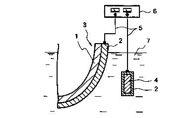
Fig. 1 is a view explaining a stain prevention apparatus
of a two-electrode system of a submerged structure in the
present invention. A conductive film 2 that does not generate
-13-
CA 02288141 1999-10-26
chlorine even by applying a potential of 5 V vs. SEC or less is
formed on a surface (stain prevention surface) in contact
with sea water or fresh water 7 in a substrate 1 of a submerged
structure. The whole body in which the conductive film 2 is
formed on the substrate 1 is called a submerged structure 3.
The conductive film will be described later.
A counter electrode substrate 4 is disposed so as not to
contact with the conductive film 2 of the submerged structure
3. A conductive film 2 that does not generate chlorine even
by applying a potential of 5 V vs . SEC or less and which is the
same as that formed on the substrate 1 of the submerged
structure is formed on the surface of the counter electrode
substrate 4. The conductive film 2 formed on the surface of
the substrate 1 of the submerged structure 3 and the
conductive film 2 formed on the surface of the counter
electrode substrate 4 are connected with a power supply unit 6
through lead wires 5. The power supply unit 6 is a unit for
passing a direct current through the conductive film 2 of the
submerged structure 3 and the conductive film 2 of the counter
electrode substrate 4, and it has a function capable of
changing the polarity.
Fig. 2 is a view explaining an example of a modified stain
prevention apparatus of a two-electrode system of a submerged
structure in the present invention. It is different from Fig.
1 in that a counter electrode is not mounted. The conductive
-14-
CA 02288141 1999-10-26
film that does not generate chlorine even by applying a
potential in sea water is formed on the surface of the
substrate 1 of the submerged structure 3. This conductive
film is divided into a conductive film 2a and a conductive
film 2b in such a state that these are completely insulated
with a fixed gap 8. This gap 8 may be filled with an
insulating material such as an inorganic substance, an
organic substance or an organic substance filled with an
inorganic substance. The conductive films 2a and 2b are
connected with the power supply unit 6 through the lead wires
5, respectively. Incidentally, when the stain prevention
surface is wide, the conductive films 2a, 2b are further
divided into many parts, whereby the effect of preventing
adhesion of organisms is more increased.
Fig. 3 is a view explaining an example in which a modified
stain prevention apparatus of the two-electrode system of the
submerged structure in the present invention is applied to a
feed water pipe . A conductive f i lm 2 a and a conductive f i lm
2b are formed on the inside of a substrate 1 of a feed water
pipe 9 in such a state that these are completely insulated
with fixed gaps 8a and 8b. Sea water or fresh water 7 is
allowed to flow within the feed water pipe 9. The gap 8a and
the gap 8b may be filled with an insulating material such as an
inorganic substance, an organic substance or an organic
substance filled with an inorganic substance. The conductive
-~s-
CA 02288141 1999-10-26
film 2a and the conductive film 2b are connected with a power
supply unit 6 respectively through lead wires 5 .
Fig. 4 is a view explaining an example in which a modified
stain prevention apparatus of the two-electrode system of the
submerged structure in the present invention is applied to a
feed water pipe assembly. In this example, a conductive film
2 is formed on the inside of each feed water pipe 9 , and a large
number of feed water pipes are connected with flanges 9a, 9b
mounted on outer surfaces of both ends of the feed water pipes
9 to provide a long feed water pipe assembly. A packing 10
made of a silicone rubber, NBR, a natural rubber or the like
having an insulating property is put in a connecting portion
between the adj acent f langes 9a, 9b to render the adj acent
conductive films 2 formed on the insides of the feed water
pipes 9 in the insulated state. By the way, the two flanges 9a,
9b of the connecting portion that hold the packing 10 are
fixed with a bolt 11 and a nut 12. Sea water or fresh water 7
is allowed to flow within the assembly of the feed water pipes
9, and the conductive films 2 of the feed water pipes 9 are
connected with a power supply unit 6 through lead wires 5,
respectively.
Fig. 5 is a view explaining an example in which a modified
stain prevention apparatus of the two-electrode system of the
submerged structure in the present invention is applied to a
fishing net such as a fixed shore net, a fish preserve or the
-16-
CA 02288141 1999-10-26
like. In a fishing net 13a and a fishing net 13b, a conductive
film that does not generate chlorine even by applying a
potential is formed on a substrate of the fishing net, and
these are located in predetermined positions by being fixed
on a frame 14 made of an insulating material. Further, the
fishing net 13a and the fishing net 13b having the conductive
films formed on the surfaces thereof are connected with a
power supply unit 6 through lead wires 5, respectively.
When a voltage by which a potential capable of killing
aquatic organisms is retained even when a conductivity of sea
water or fresh water changes is applied to the conductive film
2 in the stain prevention apparatus of the two-electrode
system shown in Fig. 1 by the power supply unit, a positive
potential is applied to the conductive film 2 formed on the
submerged structure, and a negative potential is applied to
the conductive film 2 formed on the counter electrode
substrate. At this time, the positive potential and the
negative potential are periodically applied to the
conductive film by periodically changing the polarities of
the applied potentials, whereby aquatic organisms adhered to
the surface of the conductive film can be killed and removed.
Meanwhile, in the modified examples of the stain
prevention apparatus of the two-electrode system shown in
Figs. 2 to 5, the counter electrode is dispensed with.
Accordingly, it can be used as a stain prevention apparatus of
-17-
CA 02288141 1999-10-26
a complicated submerged structure in which the counter
electrode cannot be mounted and further as a stain prevention
apparatus of a feed water pipe formed of a complicated coiled
tube having a small inner diameter.
In the conventional stain prevention apparatus of the
two-electrode system, a potential was changed owing to the
deviation from an equilibrium value of a potential due to
polarization or the change in the conductivity of sea water,
whereby it was dif f icult to accurately control a potential .
Meanwhile, in the present invention, the conductive film that
does not generate chlorine even by applying a potential in sea
water is formed on the substrate of the submerged structure,
whereby a voltage.which is high enough to be able to maintain a
potential capable of killing aquatic organisms can be applied
and effective prevention of an organism stain loss can be
conducted even when the change in the potential occurs by the
polarization or the change in the conductivity of sea water.
Further, even when a high potential is applied to the
conductive film, there is no generation of harmful chlorine
by electrolysis of sea water. Accordingly, even when the
substrate of the submerged structure is formed of a metal
having a low corrosion resistance, such as iron, aluminum or
the like, the corrosion of the substrate does not occur, nor
is there a fear of growth inhibition of cultured fish or
marine pollution.
-18-
CA 02288141 1999-10-26
By the way, in the present specification, the
"conductive film that does not generate chlorine even by
applying a potential" refers to a case where chlorine in sea
water which is measured with a residual chlorine electrode
after applying a potential to a conductive film in 50 ml of sea
water with a potentiostat for 30 minutes upon using platinum
in a counter electrode and a reference electrode as a standard
electrode is below the limit of detection.
Fig. 6 is a view explaining a stain prevention apparatus
of a three-electrode system of the submerged structure in the
invention. There is disposed a reference electrode 15 for
accurately controlling a potential applied to the conductive
film 2 formed on the surface of the substrate 1 of the
submerged structure. The reference electrode 15 is connected
with a potentiostat 16, a direct current power supply unit,
through a lead wire 5. Further, the conductive film 2 that
does not generate chlorine even by applying a potential is
formed on the surface of the counter electrode substrate 4
located so as not to contact with the conductive film 2 of the
submerged structure 3. The conductive film 2 of the substrate
1 of the submerged structure and the conductive film 2 of the
counter electrode substrate 4 are connected with the
potentiostat 16 through lead wires 5. Since a potential
capable of killing aquatic organisms is accurately applied to
the conductive film on the surf ace of the submerged structure
-19-
CA 02288141 1999-10-26
in the three-electrode system, aquatic organisms can be
controlled with good accuracy, and further a consumptive
power is also reduced as compared with the two-electrode
system. Nevertheless, the potential of the counter electrode
is not controlled. Therefore, when the surface area of the
counter electrode is smaller than the surface area of the
submerged structure, a current density of the counter
electrode is increased, and a resistance value is changed by
the change in the conductivity of scales, sea water or the
like adhered to the surface of the counter electrode to
increase the potential of the counter electrode and to cause
generation of harmful chlorine. Accordingly, the use of the
counter electrode on which surface the conductive film that
does not generate chlorine even by applying a potential is
formed makes it possible that chlorine is not generated even
by the change in the potential of the counter electrode and
that the surface area of the counter electrode is reduced, and
thus, it can be used in the stain prevention apparatus of the
complicated submerged structure.
As a material used in the counter electrode substrate 4,
thermoplastic resins such as ABS, AS, a polycarbonate, an
acrylic resin, PET, polyethylene, polypropylene, a polyimide
resin and the like, and thermosetting resins such as Bakelite,
an unsaturated polyester resin and the like are used.
Further, a metal which can be used as the conductive film 2 may
-ZO-
CA 02288141 1999-10-26
be used as such, as the counter electrode substrate 4.
Moreover, a material of a counter electrode conventionally
used in general, for example, carbon materials such as carbon,
carbon fibers, graphite and the like, iron and its alloy,
platinum, gold, rhodium, palladium, oxides thereof and the
like can be used as a material of the counter electrode. The
form of the counter electrode may appropriately be designed
according to the construction of the submerged structure,
examples thereof being mesh-like, plate-like, cylindrical
and linear forms.
Fig. 7 is a view explaining another example of a stain
prevention apparatus of a three-electrode system in the
present invention, and shows an example in which the
apparatus is located on sea or on a wide lake to which a power
cannot be supplied from land through a transmission line. It
is different from the example of Fig. 6 in a method for
supplying a power to the power supply unit. That is, as a
method for supplying a powder to a potentiostat 16, a storage
battery 17, a charging apparatus 18 and a solar battery 19 are
used, and these are connected through a lead wire 5. As the
storage battery 17, a lead storage battery, alkali storage
batteries such as a nickel-cadmium battery, a
nickel-hydrogen battery, a nickel-zinc battery, a zinc-air
battery and the like, and a lithium secondary battery are used.
The power supply unit used in the potential control in
-zi-
CA 02288141 1999-10-26
the stain prevention apparatus of the present invention is
described. The power supply unit can be a commercially
available direct current power supply in which a polarity can
periodically be converted. Further, a potentiostat is also
used. The power supply unit in the present invention is for
applying a potential to the conductive film having a wide area
at good efficiency.
A specific example of the power supply unit is described
by referring to the electrical block diagram of the overall
power supply unit shown in Fig. 8, the timing chart shown in
Fig. 9 and the electrical block diagram of the inside of the
potential control portion shown in Fig. 10. As is seen from
Fig. 8, the power supply unit comprises a data processing
portion 20 and a potential control portion 21. The timing
chart (Fig. 9) of a potential outputted from a power output
portion 26 (Fig. 10) of the potential control portion 21 and
an output time of the potential at that time is set at the data
processing portion 20. And the data of the timing chart set
at the data processing portion 20 is sent to the potential
control portion 21. In the potential control portion 21, a
potential is applied to the working electrode 22 formed of the
conductive film of the submerged structure and the counter
electrode 23 on the basis of the timing chart sent from the
data processing portion 20. Further, the potential to the
working electrode 22 and the reference electrode 15 is
- 22 -
CA 02288141 1999-10-26
inputted in the potential control portion 21, and the
potential to the working electrode 22 and the reference
electrode 15 and the actual condition of the present timing
chart are sent to the data processing portion 20. In the data
processing portion 20, the data of the sent potential to the
working electrode and the reference electrode 15 is collected,
the potential to the working electrode 22 and the reference
electrode 15 and the actual condition of the present timing
chart are analyzed, and a correction data of the potential to
the working electrode 22 and the counter electrode 23 is sent
to the potential control portion 21. Here, the working
electrode 22, the counter electrode 23 and the reference
electrode 15 are located in water.
Next, the electrical block diagram inside the potential
control portion 21 in Fig. 10 is described. The potential
control portion 21 is constructed from CPU 24, an analog input
portion 25 and a power output portion 26. In CPU 24, the data
of the timing chart of the potential applied to the working
electrode 22 and the counter electrode 23 and its time and the
correction data at that time which are sent from the data
processing portion 20 are inputted, the time indicated in the
timing chart is controlled, an output of a potential suited
for that time is indicated in the power output portion 26,
further an input of an external condition is indicated from
the analog input portion 25, and the input information is
-23-
CA 02288141 1999-10-26
outputted in the data processing portion 20. In the power
output portion 26, the potential indicated in CPU 24 is
generated through DAC (digital-to-analog converter), and a
potential is applied to the working electrode 22 and the
counter electrode 23. In the analog input portion 25, an
external condition is inputted from ADC (analog-to-digital
converter) indicated in CPU 24. For example, CPU 24 measures
a potential to the working electrode 22 and the reference
electrode 15 through ADC .
The timing chart shown in Fig. 9 is described in detail
below. The ordinate axis depicts the potential outputted
from the potential control portion 21, and the abscissa axis
depicts the time axis at that time . "+" in the ordinate axis
shows that a positive potential is applied to the working
electrode 22 and the counter electrode 23 to kill aquatic
organisms adhered to the working electrode 22. "-" shows
that a negative potential is applied to the working electrode
22 and the counter electrode 23 to remove the killed aquatic
organisms which are adhered to the working electrode 22.
With respect to a method for applying a positive potential or
a negative potential, waveforms of potentials can be changed
by various methods, for example, by gradually applying a
potential in the time axis relative to a desired potential, by
directly applying a desired potential and the like. The
timing chart of Fig. 9 shows the killing of aquatic organisms
-24-
CA 02288141 1999-10-26
adhered to the working electrode 22 for a period T1, the
removal of aquatic organisms adhered to the working electrode
22 for a period T3, a gradient to stop the killing of aquatic
organisms adhered to the working electrode 22 for a period T2,
and a gradient to stop the removal of aquatic organisms
adhered to the working electrode 22 for a period T4,
respectively.
While Fig. 8 shows the example of the power supply unit in
which the data processing portion 20 and the potential
control portion 21 are combined, Fig. 11 shows an example in
which the data processing portion 20 and the potential
control portion 21 are separated and the data processing
portion 20 controls the potential control portion 21 which is
located in a remote position. In the example of Fig. 11, it is
possible that the potential control portion 21 is, for
example, sealed in a waterproof box (not shown) and sunk in
water and the data processing portion 20 is mounted on land.
The data processing portion 20 and the potential control
portion 21 are connected through a communication line. In
the data processing portion 20, as in the example of Fig. 8,
the data of the timing chart of the set potential applied to
the working electrode 22 and the counter electrode 23 and its
time and the input data 27 from the potential control portion
21 are analyzed, the correction data is transmitted to the
potential control portion 21 as a control data 28, and the
-25-
CA 02288141 1999-10-26
data of the external condition is received from the potential
control portion 21 as an input data 27.
An example of a power supply unit shown in Fig. 12
comprises one data processing portion 20, and a plurality of
potential control portions such as a first potential control
portion 21, a second potential control portion 21a and a third
potential control portion 21b. As in the example of Fig. 11,
the communication of a control data 28 and an input data 27 is
conducted between the data processing portion 20 and each of
the potential control portions 21, 21a, 21b. In this case, it
is possible, for example, that the data processing portion 20
is mounted on land, and the first potential control portion 21,
the second potential control portion 21a and the third
potential control portion 21b are sealed in waterproof boxes,
respectively, and sunk in plural portions in water. As in the
example of Fig. 11, the data processing portion 20 is
connected with the first potential control portion 21, the
second potential control portion 21a and the third potential
control portion 21b through a communication line,
respectively. In the data processing portion 20, the data of
the timing chart of the set potential applied to the working
electrode 22 and the counter electrode 23 and its time and the
input data 27 from the plural potential control portions 21,
21a and 21b are analyzed, the correction data is transmitted
to the plural potential control portions 21, 21a, 21b as a
-26-
CA 02288141 1999-10-26
control data 28, and the data of the external condition is
received from the plural potential control portions 21, 21a,
21b as an input data 27. The data processing portion 20 and
the plural potential control portions 21 can be connected
through, for example, an interface RS-485.
An example shown in Fig. 13 illustrates, as shown in Fig.
8, a basic construction that a working electrode 22, a counter
electrode 23 and a reference electrode 15 are connected with a
potential control 21. With respect to a specific mode of each
electrode, it comprises a working electrode 22 in which a
conductive substrate is arranged in the net form ( refer to Fig.
5), a counter electrode 23 made of a plate-like conductive
substrate and a reference electrode 15 made of a bar-like
conductive substrate. These three electrodes are sunk in
water to conduct the killing and the removal of aquatic
organisms in water that are adhered to the working electrode
22.
An example shown in Fig. 14 is obtained by modifying the
construction of the example shown in Fig. 13 to provide a
plurality of reference electrodes, namely a first reference
electrode 15, a second reference electrode 15a, a third
reference electrode 15b and a fourth reference electrode 15c.
When a working electrode 22 having a larger surface area than
the net-like working electrode 22 in the example of Fig. 13 is
used, it is advisable to dispose the plural reference
_2~_
CA 02288141 1999-10-26
electrodes 15, 15a, 15b, 15c along the net-like working
electrode 22. In this case, the respective potentials to the
working electrode 22 and the plural reference electrodes 15,
15a, 15b and 15c are inputted in the analog input portion 25
(Fig. 10) of the potential control portion 21, and the data of
the respective potentials are transmitted to the data
processing portion 20 through CPU 24 (Fig. 10) of the
potential control portion 21. In the data processing portion
20, the data transmitted are collected, and analyzed; an
average value, a maximum value and a minimum value are
calculated; and the average value is made a reference value of
a potential to the working electrode 22 and the plural
reference electrodes 15, 15a, 15b and 15c. Alternatively,
one of the plural potentials to the working electrode 22 and
the plural reference electrodes 15, 15a, 15b and 15c can be
made a reference value.
Here, when the present timing chart indicates the ~~+"
side relative to the potential control portion 21, namely a
state in which a positive potential is applied to the working
electrode 22 and the counter electrode 23 to kill aquatic
organisms in water adhered to the working electrode 22 and the
maximum value exceeds the upper limit of from +0 to +1. 5 vs .
SCE, the correction data to decrease the potential to the
working electrode 22 and the counter electrode 23 is
transmitted from the data processing portion 20 to the
-28-
CA 02288141 1999-10-26
potential control portion 21 so as to render the maximum value
within the range of from +0 to +1.5 V vs. SCE. Unless the
maximum value exceeds the upper limit, that condition is
maintained. Further, when the timing chart indicates the ~~-~~
side relative to the potential control portion 21, namely a
state in which a negative potential is applied to the working
electrode 22 and the counter electrode 23 to remove aquatic
organisms in water adhered to the working electrode 22 and the
minimum value is less than the lower limit of from -0 to -0. 4 V
vs. SCE, the correction data to increase the potential to the
working electrode 22 and the counter electrode 23 is
transmitted from the data processing portion 20 to the
potential control portion 21 so as to render the minimum value
within the range of from -0 to -0.4 V vs. SCE. Unless the
minimum value is less than the lower limit, that condition is
maintained.
In an example shown in Fig. 15, a temperature sensor 29
for detecting a water temperature and a pH sensor 30 for
detecting an acidity in water are added to the construction of
the example shown in Fig. 13, and these sensors are
electrically connected with the analog input portion 25 (Fig.
) of the potential control portion 21. Since a potential is
applied to the working electrode 22 and the counter electrode
23, there is a possibility of causing electrolysis in water,
e.g. in sea water to change the acidity. Therefore, the
-29-
CA 02288141 1999-10-26
change in the acidity can be detected by the pH sensor 30. The
data from the temperature sensor 29 and the pH sensor 30 are
inputted into the analog input portion 25 of the potential
control portion 21, and transmitted to the data processing
portion 20 through CPU 24. In the data processing portion 20,
the data transmitted are collected, and analyzed.
When it is judged in the data processing portion 20 that
the data of the temperature sensor 29 is a water temperature
indicating an activity of aquatic organisms in water and the
present timing chart indicates the "+" side relative to the
potential control portion 21, namely a state in which a
positive potential is applied to the working electrode 22 and
the counter electrode 23 to kill aquatic organisms in water
adhered to the working electrode 22, the correction data to
increase the potential to the working electrode 22 and the
counter electrode 23 is transmitted from the data processing
portion 20 to the potential control portion 21 so as to render
the potential to the working electrode 22 and the counter
electrode 23 within the range of from +0 to +1.5 V vs. SCE.
Further, when the present timing chart indicates the "-" side
relative to the potential control portion 21, namely a state
in which a negative potential is applied to the working
electrode 22 and the counter electrode 23 to remove aquatic
organisms in water adhered to the working electrode 22, the
correction data to decrease the potential to the working
-30-
CA 02288141 1999-10-26
electrode 22 and the counter electrode 23 is transmitted from
the data processing portion 20 to the potential control
portion 21 so as to render the potential to the working
electrode 22 and the counter electrode 23 within the range of
from -0 to -0 . 4 V vs . SCE .
Although the foregoing description is with respect to
the correction data for changing the potential to the working
electrode 22 and the counter electrode 23, the correction
data for changing a potential application time can also be
used. That is, when it is judged in the data processing
portion 20 that the data of the temperature sensor 29 is a
water temperature indicating an activity of aquatic
organisms in water and the present timing chart indicates the
°+" side relative to the potential control portion 21, namely
a state in which a positive potential is applied to the
working electrode 22 and the counter electrode 23 to kill
aquatic organisms in water adhered to the working electrode
22, the correction data to prolong a time of applying a
potential to the working electrode 22 and the counter
electrode 23 in the range of from +0 to +1.5 V vs. SCE is
transmitted from the data processing portion 20 to the
potential control portion 21 so as to prolong the time of
applying a potential to the working electrode 22 and the
counter electrode 23. Further, when the present timing chart
indicates the "-" side relative to the potential control
-31-
CA 02288141 1999-10-26
portion 21, namely a state in which a negative potential is
applied to the working electrode 22 and the counter electrode
23 to remove aquatic organisms in water adhered to the working
example 22, the correction data to prolong a time of applying
a potential to the working electrode 22 and the counter
electrode 23 in the range of from -0 to -0.4 V vs. SCE is
transmitted from the data processing portion 20 to the
potential control portion 21 so as to prolong the time of
applying a potential to the working electrode 22 and the
counter electrode 23.
Likewise, when a data according to the pH sensor 30 shows
a limit value at which to start electrolysis in the data
processing portion 20 and the present timing chart indicates
the ~~+" side relative to the potential control portion 21,
namely a state in which a positive potential is applied to the
working electrode 22 and the counter electrode 23 to kill
aquatic organisms in water adhered to the working electrode
22, the correction data to decrease the potential to the
working electrode 22 and the counter electrode 23 is
transmitted from the data processing portion 20 to the
potential control portion 21 so as not to cause electrolysis .
Further, when the present timing chart indicates the "-" side
relative to the potential control portion 21, namely a state
in which a negative potential is applied to the working
electrode 22 and the counter electrode 23 to remove aquatic
-32-
CA 02288141 1999-10-26
organisms in water adhered to the working electrode 22, the
correction data to increase the potential to the working
electrode 22 and the counter electrode 23 is transmitted from
the data processing portion 20 to the potential control
portion 21. However, when the temperature sensor 29 and the
pH sensor 30 are both mounted, the data of the pH sensor 30 is
preferentially transmitted to the potential control portion
21 whereby the data processing portion 20 treats most
preferentially the case where the data from the pH sensor 30
indicates the limit value at which to start electrolysis .
The substrate of the submerged structure used in the
stain prevention apparatus of the present invention is
described below.
Fig. 16 and Fig. 17 are views that schematically show an
example of a laminated structure of a substrate 1 and a
conductive film 2 in which the substrate of the submerged
structure is made of a material that is not dissolved nor
corroded electrochemically. As the substrate 1, a metallic
material, a resin material, an inorganic material and a
natural material can be used. As the metallic material,
valve metals such as titanium and its alloy, tantalum and its
alloy, zirconium and its alloy, niobium and its alloy, and the
like are mentioned. Since these valve metals can be used also
as a material of the conductive film 2, it is also possible
that the substrate 1 of the submerged structure and the
-33-
CA 02288141 1999-10-26
conductive film 2 are integrated and produced from the valve
metals. As the resin material, ABS, AS, polyester,
polystyrene, polycarbonate, polyethylene, polypropylene,
nylon, vinyl chloride, PET, FRP, aliphatic polyamides such as
6-nylon, 6,6-nylon, 1,2-nylon and the like, aromatic
polyamides such as nomex and the like, alicyclic polyamides
such as Kevler and the like, and so forth are mentioned. As
the inorganic material, glass, alumina, zirconia, cement,
graphite, carbon fibers and the like are mentioned. As the
natural material, wood, stone, silk, cotton, hemp and the
like are mentioned. The form of these materials is not
particularly limited so long as it is a fibrous form or a form
having a function of maintaining the structure .
Fig. 16 is an example in which the conductive film 2 is
directly formed on the surface of the submerged structure 1.
Fig. 17 is an example in which the conductive film 2 is
laminated on the substrate 1 through an adhesive layer la.
Incidentally, the adhesive used in the adhesive layer la
includes a pressure-sensitive adhesive, a hot-melt adhesive,
an anaerobic adhesive and the like, and these may be used
either alone or in admixture of two or more .
Figs. 18 to 21 are views that schematically show an
example of a laminated structure of the substrate 1 and the
conductive film 2 when the substrate of the submerged
structure is made of a material that is dissolved or corroded
-34-
CA 02288141 1999-10-26
v y
electrochemically. Examples of the material that is
dissolved or corroded include metallic materials such as iron
and its alloy or stainless steel, aluminum and its alloy,
copper and its alloy, zinc and its alloy, magnesium and its
alloy, and so forth. Fig. 18 shows an example of a laminated
structure in which an insulating layer lb is interposed
between these substrates 1 and the conductive film 2 formed on
the water contact surface. As the material of the insulating
layer lb, inorganic insulating materials made of oxides such
as alumina, zirconia, titanium oxide, silicon oxide and the
like, insulating resins such as an unsaturated polyester
resin, an acrylic-urethane resin, a polyester-urethane resin,
a silicone-urethane resin, a silicone-acrylic resin, an
epoxy resin, a thermosetting melamine-alkyd resin, a
melamine-acrylic resin, a melamine-polyester resin, an
acrylic resin, an acrylic-urethane resin, a polyimide resin
and the like, insulating resin films made of a polyethylene
resin, a polypropylene resin, a polyester resin, a polyimide
resin, a polystyrene resin, a fluorocarbon resin, a PTFE
resin and the like, and so forth are mentioned.
Fig. 19 is an example in which an insulating layer lb is
formed on the substrate 1 and the conductive film 2 is
laminated on this insulating layer lb through an adhesive
layer lc . With respect to materials of the insulating layer
lb and the adhesive layer lc, the same insulating material and
-35-
CA 02288141 1999-10-26
i ,
adhesive as those described in the lamination example of Fig.
17 can be used.
Fig. 20 is an example in which an insulating layer
(insulating resin film in this example) lb is formed on the
substrate 1 through the same adhesive layer lc as the
above-mentioned and the conductive film 2 is laminated on
this insulating layer lb. Further, Fig. 21 is an example in
which an adhesive layer lc is further interposed between the
insulating layer lb and the conductive film 2 in the laminated
structure of Fig. 20.
Next, the conductive film 2 formed on the water contact
surface of the submerged structure is described. The
conductive film used in the present invention is formed of a
metal or its compound in which chlorine is not generated even
by applying a potential of 5 V vs. SCE or less. As the metal,
valve metals, specifically, titanium and its alloy, tantalum
and its alloy, zirconium and its alloy, niobium and its alloy,
vanadium and its alloy, hafnium and its alloy, molybdenum and
its alloy, tungsten and its alloy, and so forth are mentioned.
These valve metals can be used as a film having a thickness of
0.1 ,Clm or more. The upper limit of the thickness is not
particularly restricted, and it can appropriately be
determined depending on a method for forming a conductive
film or a use purpose. By the way, with respect to the valve
metal used as the conductive film, a thin oxide coating film
-36-
CA 02288141 1999-10-26
t r
may be formed on its surface. Further, it may contain two or
more metals, and oxides, nitrides, carbides and the like of
these metals depending on the forming method.
As the conductive film 2 of the submerged structure, one
or more types of metallic compounds such as a metal nitride, a
metal carbide, a metal boride, a metal silicide and the like
can be used. As the metal nitride, titanium nitride,
zirconium nitride, vanadium nitride, tantalum nitride,
niobium nitride, chromium nitride and the like are mentioned.
As the metal carbide, titanium carbide, zirconium carbide,
vanadium carbide, niobium carbide, tantalum carbide,
chromium carbide, molybdenum carbide, tungsten carbide and
the like are mentioned. As the metal boride, titanium boride,
zirconium boride, hafnium boride, vanadium boride, niobium
boride, tantalum boride, chromium boride, molybdenum boride,
tungsten boride and the like are mentioned. As the metal
silicide, titanium silicide, zirconium silicide, niobium
silicide, tantalum silicide, vanadium silicide, tungsten
silicide and the like are mentioned. These metallic
compounds can be used as a film having a thickness of 0. 1 ,CC m
or more. The upper limit of the thickness is not particularly
restricted, and it can appropriately be determined depending
on a method for forming a conductive film or a use purpose.
Incidentally, these metallic compounds can also be used in
admixture of two or more, and may further contain two or more
-37-
CA 02288141 1999-10-26
metals, oxides thereof and the like depending on the forming
method.
The method in which the conductive film formed of the
valve metal or the metallic compound such as the metal nitride,
the metal carbide, the metal boride, the metal silicide or the
like is formed on the substrate of the submerged structure can
appropriately be selected depending on the use purpose. For
example, a physical deposition method such as sputtering or
ion plating, and a spraying method such as plasma spraying,
arc spraying, low-pressure spraying, low-temperature
spraying or the like can be employed. In the formation of the
conductive film formed of the metal nitride, the metal
carbide, the metal boride or the metal silicide, for example,
the following methods can be employed. With respect to the
metal nitride, metals constituting the metal nitride, such as
titanium, zirconium, tantalum, chromium and the like are
treated by an ion nitriding method in which these are treated
with nitrogen ion in vacuum under bias, a gas nitriding method
in which these are heat-treated in air in an atmosphere of
nitrogen or ammonia gas, a salt bath nitriding method in which
these are dipped in a molten salt containing NaCN or NaCNO or
the like, whereby a nitride film can be formed on the surfaces
of these metals. With respect to the metal carbide, metals
constituting the metal carbide, for example, titanium,
zirconium, tantalum, chromium and the like are treated by a
-38-
CA 02288141 1999-10-26
f
gas carbonization method in which these are heat-treated in
an atmosphere of a CO-containing gas, a salt bath
carbonization method in which these are dipped in a molten
salt composed mainly of NaCN, an electrolytic carbonization
method in which cathode electrolysis is conducted in a molten
salt composed mainly of a carbonate such as Na~C03 or the like,
whereby a carbide film can be formed on the surfaces of these
metals. With respect to the metal boride, metals
constituting the metal boride, such as titanium, zirconium,
niobium, tantalum and the like are treated by a gas boronizing
method in which these are heat-treated in an atmosphere of a
gas containing hydrogen and diborane, a melt-boronizing
method in which these are dipped in a molten salt composed
mainly of borax, an electrolytic boronizing method in which
cathode electrolysis is conducted in a molten salt composed
mainly of borax or the like, whereby a boride film can be
formed on surfaces of these metals . With respect to the metal
silicide, the metals constituting the metal silicide are
treated by a siliconizing method in which heat treatment is
conducted in an atmosphere of a mixed gas of SiCla and hydrogen
or nitrogen, whereby a silicide film can be formed on the
surfaces of the metals .
In the stain prevention apparatus of the present
invention, a submerged structure in which a sprayed coating
film formed of a metal nitride is formed as the conductive
-39-
CA 02288141 1999-10-26
~
film on the substrate of the submerged structure can be used
especially preferably. Figs. 22 to 25 are views that
schematically show an example of a laminated structure in
which a sprayed coating film of a metal nitride is formed on
the substrate 1 of the submerged structure.
Fig. 22 is an example in which the substrate 1 is formed
of a material other than the metal, such as a resin material,
an inorganic material or a natural material, a fiber layer le
is laminated on the surface of such a substrate 1 through an
adhesive layer ld and the conductive film 2 made of the metal
nitride is formed on this fiber layer le by spraying. When
the substrate 1 is a resin, it is advisable to form fine
raisings and depressions (not shown) on the surface of the
substrate 1 by blast treatment or chemical etching treatment
in order to enhance an adhesion strength between the
substrate 1 and the adhesive layer ld though it depends on the
type of the resin or the type of the adhesive .
As the adhesive used in the adhesive layer ld, any type of
the adhesive can be used so long as it is excellent in the sea
water resistance or the water resistance. For example, a
pressure-sensitive adhesive, hot-melt adhesive, a two
component curable adhesive, an anaerobic adhesive and the
like are mentioned. Such an adhesive layer ld can be formed
by a spraying method, brush coating, a roll coater method or
the like .
-40-
CA 02288141 1999-10-26
As the fiber layer 1e, any of a natural fiber, an
inorganic fiber and a synthetic fiber, or a fabric or a mesh
woven by mixing these fibers is used. As the natural fiber,
cotton, hemp, silk, wool and the like are mentioned. As the
inorganic fiber, asbestos, a glass fiber, a carbon fiber and
the like are mentioned. As the synthetic fiber, a viscose
rayon, an acetate fiber, a polyamide-based fiber (aliphatic
polyamide, aromatic polyamide or alicyclic polyamide), a
polyester-based fiber (polyethylene terephthalate fiber), an
acrylonitrile-based fiber, a modacrylic fiber, a polyvinyl
chloride-based fiber, a polyvinylidene chloride-based fiber,
a polyolefin-based fiber ( polyethylene fiber or
polypropylene fiber) , a polyurethane-based fiber,
polychlal-based fiber, a fluorocarbon-based fiber, a
polyglycol fiber, a phenol-based fiber and the like are
mentioned.
Figs . 23 to 25 show examples of a laminated structure in
which the substrate 1 is formed of a metal. In Fig. 23, the
adhesive layer ld is formed on the substrate 1 through the
insulating layer lb, the fiber layer le is laminated on the
adhesive layer ld, and the conductive film 2 made of the metal
nitride is formed on the surface of the fiber layer le by
spraying. The insulating layer lb is interposed between the
substrate 1 and the adhesive layer 1d for improving the
adhesion therebetween. The insulating layer 1 is interposed
-41-
CA 02288141 1999-10-26
to prevent corrosion or dissolution of the substrate 1
because when a potential is applied to the conductive film 2
in water or in sea water, corrosion or dissolution occurs in
some type of the metal of the substrate 1 and the fiber layer
le is sometimes peeled off . Further, as required, the metal
surface of the substrate 1 may be roughened by blast treatment
or etching treatment, or low-boiling metallic materials such
as aluminum and its alloy, zinc and its alloy, magnesium and
its alloy, nickel and its alloy, chromium and its alloy, and
so forth may be formed on the surface of the metal by spraying
or plating.
Fig. 24 shows an example in which after the insulating
layer lb made of an insulating coating film is formed on the
substrate 1, the fiber layer le is laminated through the
adhesive layer ld and the conductive film 2 made of the metal
nitride is formed on the surface of the fiber layer le by
spraying.
Fig. 25 shows an example in which the insulating layer lb
made of the insulating resin film is laminated on the
substrate 1 through the adhesive layer lc, the fiber layer le
is laminated on the insulating layer lb through the adhesive
layer ld, and the conductive film 2 made of the metal nitride
is formed on the surface of the fiber layer le by spraying.
In the lamination examples of Figs. 26 to 28, not the
fiber layer le used in the lamination examples of Figs. 22 to
-42-
CA 02288141 1999-10-26
25 but a resin layer if containing an inorganic powder having
a particle diameter of from 10 to 200 ,(,C m is used. The
inorganic powder contained in the resin layer if includes
alumina, zirconia, silicon oxide and titanium oxide, and
these can be used alone or in admixture of two or more. The
inorganic powder is mixed within the range of from 10 to 300
by weight based on the solid content of the resin used. As the
resin used in the resin layer lf, a two component curable
unsaturated polyester resin, an acrylic-urethane resin, a
polyester-urethane resin, a silicone-urethane resin, a
silicone-acrylic resin, an epoxy resin, a thermosetting
melamine-alkyd resin, a melamine-acrylic resin, a
melamine-epoxy resin, an acrylic resin, an acrylic-urethane
resin and the like are mentioned. These can be used alone or
in admixture of two or more. This resin layer if can be formed
by coating the resin by a spraying method, a brush coating
method, a roll coater method or the like, and then conducting
air-drying or heat-drying.
Fig. 26 is an example in which the resin layer if is
formed on the substrate 1 made of a resin and the conductive
film 2 made of the metal nitride is then formed by spraying.
By the way, in this example, the surface of the substrate 1
made of the resin is roughened by blast treatment or chemical
etching to enhance the adhesion between the substrate 1 and
the resin layer if .
-43-
CA 02288141 1999-10-26
Fig. 27 is an example in which the insulating layer lb
made of the insulating coating film is formed on the substrate
1 made of the metal, the resin layer if is then formed through
the adhesion layer ld, and the conductive film 2 made of the
metal nitride is formed on the surface of the resin layer 1f by
spraying.
Fig. 28 is an example in which the insulating layer lb
made of the insulating resin film is laminated on the
substrate 1 made of the metal through the adhesive layer lc,
the resin layer if is formed on the insulating layer lb
through the adhesive layer ld and the conductive film 2 made
of the metal nitride is formed on the surface of the resin
layer if by spraying.
A method in which the above-mentioned conductive film
made of the sprayed coating film of the metal nitride is
formed on the stain prevention surface of the submerged
structure is described below.
Fig. 29 shows a sprayer for spraying the metal nitride by
a low-temperature spraying method. This sprayer comprises a
high-frequency spray gun 31, a high-frequency direct current
power supply 32, a compressor 33, a cooler 34 and a spray metal
wire supply device having spools 35a, 35b. The spray gun 31
has two sets of feed rollers 38a, 38b for separately feeding
spray metal wires 36a, 36b from the gun to a tip of a nozzle 37 .
When the spray metal wires 36a and 36b to which different
-44-
CA 02288141 1999-10-26
polarities are imparted with the high-frequency direct
current power supply 32 are contacted at a spray metal wire
melting portion 39, an electrical arc is generated, and the
spray metal wires 36a, 36b are melted with this electrical arc.
Meanwhile, a nitrogen-containing gas is fed from a
container 41 f filled with a nitrogen gas and an ammonia gas to a
cooler 34 through a connecting pipe 42 to cool the same, and it
is compressed with a compressor 33. The cooled
nitrogen-containing compressed gas is introduced into the
spray gun 31 through an introduction pipe 43, and fed in an
arrow direction through a gap 40, reaching the spray metal
wire melting portion 39. When the gas is passed through this
portion as a high-speed stream, the pressure is reduced, and
the metal melted in this melting portion 39 is pulverized. By
the way, the cooled nitrogen-containing compressed gas
introduced into the spray gun 31 is fed to the spray metal wire
melting portion 39 also through a gap 44. The gap sectional
areas are adjusted such that an amount of the compressed gas
passed through the gap 40 is larger than that passed through
the gap 44.
The pressure-reduced molten metal particles 45 in the
spray wire melting portion 39 are contacted with the
high-speed stream of the cooled nitrogen-containing
compressed gas fed through the gap 40 and the cooled
nitrogen-containing compressed gas fed through the gap 44 in
-45-
CA 02288141 1999-10-26
the arrow direction, and the surfaces of the particles are
nitrided to form nitrides. The nitrided molten metal
particles 45 are flown toward a substrate 46 ( substrate of a
submerged structure on which a sprayed coating film is to be
formed) along with the high-speed stream of the cooled
nitrogen-containing compressed gas from the gap 40. The
molten metal particles 45 are, when flown along with the
high-speed stream, abruptly cooled to be in a supercooled
state. Since the molten metal particles 45 in this
supercooled state are in the molten state at a low temperature,
these are struck against the surf ace of the substrate 4 6 , and
piled on that surface to form a sprayed coating film of the
metal nitride.
As stated above, the molten metal particles are rendered
in the supercooled state whereby oxidation of the surfaces of
the molten metal particles is extremely suppressed and
further the substrate of the resin or the like is not deformed
when the metal particles being in the molten state at a low
temperature are struck against the surface of the substrate
to form the sprayed coating film. Further, the spray metal
wire melting portion 39 at which the spray metal wires 36a,
36b are contacted and melted is put under reduced pressure and
a high-frequency voltage is applied by a high-frequency
direct current power source 32, making it possible to easily
spray a metallic material having a high-melting point. By
-46-
i
CA 02288141 1999-10-26
the way, the high frequency of the high-frequency voltage to
be applied is preferably within the range of from 20 kHz to 200
kHz. When it is less than 20 kHz, the metallic material
having a high-melting point cannot be melted at good
efficiency at times. When it exceeds 200 kHz, the spray metal
wires are melted and broken, and cannot continuously be
sprayed at times .
The potential application conditions in the
electrochemical control of organisms using the
electrochemical stain prevention apparatus of the present
invention are described. When a potential is applied to the
conductive film formed on the stain prevention surface of the
submerged structure, it is recommendable to periodically
apply a positive potential and a negative potential.
First, application of a positive potential is described.
Organisms in water can be adsorbed on the surface of the
conductive film by applying a positive potential of from +0. 1
V vs. SCE to +5.0 V vs. SCE to the conductive film of the
submerged structure. Further, the positive potential to be
applied to the conductive film has a function of
electrochemically killing organisms adsorbed on the surface
of the conductive film. When the applied potential is less
than .+0.1 V vs. SCE, organisms cannot be adsorbed on the
conductive film and killed. Further, when a potential
exceeding +5.0 V vs. SCE is applied, a thick oxide coating
-47-
CA 02288141 1999-10-26
film having a high insulating property is, in some cases,
formed on the surface of the conductive film or the conductive
film is deteriorated. Thus, no desired effect is obtained.
It is preferable that the application time of the positive
potential is between 1 minute and 6 hours. When the
application time exceeds 6 hours, other organisms are
sometimes adsorbed on organisms killed on the surface of the
conductive film of the submerged structure. Organisms
adsorbed later are not directly contacted with the conductive
film, and therefore do not undergo the electrochemical
killing action by the positive potential.
Incidentally, when the positive potential of from +0.1 V
vs. SCE to +5.0 V vs. SCE is applied to the conductive film
(working electrode) in the stain prevention apparatus of the
two-electrode system, it is advisable to apply the potential
of from 0.3 V to 7.5 V to the counter electrode.
Aquatic organisms adhered to the conductive film were
electrochemically controlled or killed so far mainly through
the electron transfer reaction between cells and the
conductive film by applying a relatively low potential of 1.5
V or less . On the other hand, in the present invention, since
the conductive film is used which does not allow generation of
harmful chlorine even by applying a relatively high potential
of +5.0 V vs. SCE, it has been possible to apply the relatively
high potential of +1. 5 V vs . SCE or more to the conductive film.
-48-
CA 02288141 1999-10-26
When such a high potential is applied, water is hydrolyzed to
form an OH radical. The OH radical has quite a high oxidation
activity and can destroy cell membranes of organisms adhered
to the surface of the conductive film, influence DNA in cells
and kill organisms. Accordingly, in the present invention,
this OH radical can positively be utilized to
electrochemically control or kill aquatic organisms. Since
the OH radical generated this time has quite a short life,
there is no pollution of sea water or fresh water.
Therefore, according to the present invention, when a
potential in a wide range of from +0 .1 V vs . SCE to +5 . 0 V vs .
SCE is applied to the conductive film, it is possible to
electrochemically control or kill aquatic organisms more
effectively by both of the actions, the ordinary electron
transfer reaction between cells and electrode by the
application of the relatively low potential and the OH
radical generated through electrolysis of water by the
application of the relatively high potential. Meanwhile,
when the potential in the relatively limited range of from
+1. 5 V vs . SCE to +5 V vs . SCE is applied to the conductive film,
the control or the killing by the OH radical is preferentially
carried out, rather than by the electron transfer reaction
between cells and electrode. Therefore, it is possible to
control or kill organisms for a short period of time using the
OH radical having a strong oxidation activity.
-49-
CA 02288141 1999-10-26
After the application of the positive potential, the
negative potential of f rom -0 . 1 V vs . SCE to -2 . 0 V vs . SCE is
applied to the conductive film, making it possible to remove
organisms adsorbed and killed on the surface of the
conductive film. When the applied potential is higher than
-0.1 V vs. SCE, organisms cannot be removed from the surface
of the conductive film. When it is lower than -2 . 0 V vs . SCE,
the pH is increased, and it is therefore undesirable. The
time for applying the negative potential is preferably
between 1 minute and 2 hours. When the application time
exceeds 2 hours, it is impossible to effectively kill
organisms.
Incidentally, when the negative potential of from -0. 1 V
vs. SCE to -2.0 V vs. SCE is applied to the conductive film
(working electrode) in the stain prevention apparatus of the
two-electrode system, it is advisable to apply a voltage of
from 0.3 to 7.5 V to the counter electrode.
The present invention is specifically illustrated by
referring to the following Examples.
Formation of a conductive film of a submerged structure
Example 1
A surface of a polyethylene terephthalate (PET) resin
plate (30 x 50 x 5 mm) was dipped in an aqueous solution of 60 °C
containing 200 g/L (liter) of chromic acid and 550 g/L of
sulfuric acid for 60 minutes to conduct etching.
-50-
CA 02288141 1999-10-26
Subsequently, 100 g of a polyester-based adhesive
("PES-360SSK" made by Toagosei Co., Ltd.) and 10 g of an
isocyanate-based curing agent ("Coronate L" made by Nippon
Polyurethane Industry Co., Ltd.) were mixed. Two-hundred
percent by weight, based on the resin solid content of the
resulting mixture, of an alumina powder having a mean
particle size of 70 ,(.gym (made by Japan Abrasive Co., Ltd.)
were added, and 150 g of a mixed solvent (toluene : MEK = 8 : 2)
were added. The mixture was stirred well. The resin
composition thus obtained was coated on the surface of the
etched PET resin by a spraying method, and dried at 90 °C for 60
minutes. Then, titanium was sprayed under the following
conditions using the sprayer ( "PC250iDEX" supplied by
Arctechno Co., Ltd.) shown in Fig. 29. As titanium, a pure
titanium wire having a diameter of 1.3 mm was used. A
high-frequency voltage was applied at 40 kHz and 14 V. Air
cooled to 11 °C was introduced into a spray gun at a pressure of
8 kg/cm~ and a titanium wire was fed at a feed rate of 5. 2 m/min
to form a sprayed coating film of titanium nitride having a
thickness of 200 ,Cl m on the PET resin. The resulting sprayed
coating film had a light yellow color.
Example 2
A surface of a cement plate (30 x 50 x 5 cm) was roughened
by blast treatment, and then titanium was sprayed under the
same conditions as in Example 1 using the sprayer used in
-si-
CA 02288141 1999-10-26
Example 1 to form a sprayed coating film of titanium nitride
having a thickness of 200 ,u m on the cement plate. While the
spraying was conducted using cooled air in Example 1, it was
conducted under the same condition of the gas pressure as in
Example 1 by replacing cooled air with a nitrogen gas. The
resulting sprayed coating film had a light yellow color.
Example 3
A surface of a stainless steel plate (30 x 50 x 1 mm) was
roughened by sand blast treatment. Alumina was then sprayed
on the stainless steel in a nitrogen gas ( f low rate : 100 L/min)
by an ordinary plasma jet spraying method to form an alumina
sprayed coating film having a thickness of 100 ,(.L m.
Subsequently, titanium was sprayed using the same sprayer as
in Example 2 under the same conditions to form a sprayed
coating film of titanium nitride having a thickness of 200 ,u m
on the alumina coating film. The resulting sprayed coating
film had a light yellow color.
Example 4
A surface of an FRP plate (30 x 50 x 10 mm) was roughened
by sand blast treatment. Subsequently, 100 g of a
silicon-acrylic resin ("Beltight 6000" made by Nippon Oil &
Fats Corp. ) and 200$ by weight, based on the solid content of
the silicon-acrylic resin, of an alumina powder having a mean
particle size of 70 ,Clm (made by Japan Abrasive Co., Ltd.)
were mixed. The mixture was stirred well. To the resulting
-52-
CA 02288141 1999-10-26
resin composition were added an exclusive curing agent and an
exclusive thinner. The resulting mixture was coated on the
surface of the etched FRP resin by a spraying method, and
dried at 100 °C for 60 minutes. Subsequently, a sprayed
coating film of titanium nitride having a thickness of 150 ,u m
was formed under the same conditions as in Example 1 except
that a mixed gas of a nitrogen gas and an ammonia gas (nitrogen
gas : ammonia gas = 10 : 1 in volume ratio) was introduced to a
spray gun at 8 kg/cm~. The resulting sprayed coating film had
a light yellow color.
Example 5
A sprayed coating film of titanium nitride having a
thickness of 200 ,CC m was formed on a surface of an FRP plate
(30 x 50 x 10 mm) under the same conditions as in Example 4
except that the mixed gas of the nitrogen gas and the ammonia
gas used in Example 4 was replaced with a mixed gas of air and
an ammonia gas (air : ammonia gas = 5 : 1 in volume ratio) . The
resulting sprayed coating film had a light yellow color.
Example 6
A surface of an FRP plate ( 30 x 50 x 5 mm) was roughened
using an emery paper (#100). To 100 parts by weight of a
polyester-based adhesive ("PES-360SSK") were added 5 parts
by weight of an isocyanate-based curing agent ( "Coronate L" )
and 100 parts by weight of a solvent (toluene : MEK = 8 : 2 ) ,
and the mixture was stirred and mixed well. This adhesive was
-53-
CA 02288141 1999-10-26
coated on the roughened FRP surface by a spraying method, and
then dried at 80°C for 10 minutes. Subsequently, a fabric
("H201M104F" made by Unitika Glass Fiber Co. , Ltd. ) obtained
by weaving glass fibers was placed on the FRP coated with the
adhesive, and heat-pressed at 200°C and a pressure of 10 kg/cmZ
for 2 minutes. Then, a sprayed coating film of titanium
nitride having a thickness of 200 ,CL m was formed on the glass
fiber fabric under the same conditions as in Example 1 using
the sprayer used in Example 1.
Example 7
The adhesive used in Example 1 was coated on a surface of
a nylon plate (30 x 50 x 5 mm) under the same conditions as in
Example 6. Subsequently, a fabric ("KE3033" made by Du
Pont-Toray-Kevlar Co., Ltd.) obtained by weaving
polyaramid-based fibers was heat-pressed on the nylon plate
having the adhesive coated thereon under the same conditions
as in Example 6. Then, titanium was sprayed onto the
polyaramid-based fiber fabric using the sprayer used in
Example 1. While the spraying was conducted under the
condition of the air pressure of 8 kg/cm~ in Example 6, the
conditions were the same as in Example 1 except that air was
replaced with a nitrogen gas and the gas pressure was 15 kg/cm~.
As a result, a sprayed coating film of titanium nitride
having a thickness of 200 ,(,C m was formed on the
polyaramid-basedfiber fabric.
-54-
CA 02288141 1999-10-26
Example 8
A surface of a stainless steel plate (30 x 50 x 1 mm) was
roughed by sand blast treatment. Subsequently, alumina was
sprayed on the stainless steel plate in a nitrogen gas ( flow
rate : 10 0 L/min ) by an ordinary plasma j et spraying method to
form an alumina sprayed coating film having a thickness of 100
,Clm. A two component curable epoxy-based adhesive ("Bond
Quick" made by Konishi Co., Ltd.) was coated on the alumina
sprayed coating film, and a fabric ("C0641" made by Toray
Industries , Inc . ) obtained by weaving carbon f fibers was then
laminated. Thereafter, titanium was sprayed under the same
conditions as in Example 7 using the sprayer used in Example 1
to form a sprayed coating film having a thickness of 200 ,(.C m on
the carbon f fiber f abric .
Comparative Example 1
After the surface of the FRP plate used in Example 6 was
roughened with an emery paper (#100), titanium was sprayed
under the same conditions as in Example 1 using the sprayer
used in Example 1. A titanium nitride coating film was little
formed on the FRP surface.
Comparative Example 2
After the surface of the nylon plate used in Example 2 was
roughened by sand blast treatment, titanium was sprayed under
the same conditions as in Example 1 using the sprayer used in
Example 1. A titanium nitride coating film was not formed on
-55-
CA 02288141 1999-10-26
the surface of the nylon plate, and the nylon plate was
deformed.
Analysis of sprayed coating films
The sprayed coating films obtained in Examples 1 to 8
were analyzed by the X-ray diffraction method. The X-ray
dif fraction was conducted at an angle of incidence of 0 . 2° by a
thin film method using CuK GY as an X-ray. As a result, a
diffraction peak ascribable to TiN was observed in the
sprayed coating films obtained in Examples 1 to 8, and it was
identified that the titanium nitride coating film was formed
by the method of the present invention.
Evaluation of a durability of sprayed coating films
A member having the titanium nitride sprayed coating
film obtained in each of Examples 1 to 8 was used as a working
electrode, and its durability was evaluated. A test device
shown in Fig. 30 was used in the test for evaluation of the
durability. The working electrode formed of the member 48
having the titanium nitride sprayed coating film obtained in
each of Examples 1 to 8, a counter electrode 23 formed of a
platinum plate and a reference electrode 15 formed of a
saturated calomel electrode (SCE) are arranged in a test tank
47 filled with 500 mL of sea water, and each of the electrodes
is electrically connected with a potentiostat 16. Further,
the potentiostat 16 is electrically connected with a function
generator 49. A stirring device 50 and a stirrer 51 are
-56-
CA 02288141 1999-10-26
a r
disposed on the bottom of the test tank 47.
A fixed potential of 1.0 V vs. SCE was continuously
applied to the working electrode of the test device of such a
structure for 3 days. An amount of a metal eluted from the
surface of the sprayed coating film of the working electrode
formed of the member 48 was measured by ICP spectroscopy, and
a resistance value of the sprayed coating film on the member
48 was measured using a multimeter ( "73 Multimeter" supplied
by ,john Fluke Mfg. Co. , Inc. ) . The test results are shown in
Table 1.
Table 1
Type of Metal eluted Change in
member from sprayed
coatin film resistance value
m)
Example 1 below the limitof detectionno change
Example 2 below the limitof detectionno change
Example 3 below the limitof detectionno change
Example 4 below the limitof detectionno change
Example 5 below the limitof detectionno change
Example 6 below the limitof detectionno change
Example 7 below the limitof detectionno change
[Identification of a killing effect
Example 9
Marine bacteria Vibrio alginolyticus were used as
aquatic organisms. The marine bacteria were aerobically
incubated in a synthetic medium ( "Marine broth 2216" made by
DIFCO Laboratory Co. , Ltd. ) at 25°C for 10 hours . After the
-57-
CA 02288141 1999-10-26
a
incubation, the cells were centrifugally collected, then
washed with sterile sea water, and suspended in sterile sea
water. The number of cells was counted using a hematite meter.
A cell suspension having a concentration of 1 x 10⁸ cells/mL
was prepared, and used in the test . The member obtained in
each of Examples 1 to 8 was dipped in the cell suspension
having the concentration of 1 x 10⁸ cells/mL for 90 minutes,
and the marine bacteria were adsorbed on the surface of the
conductive film of the member. Subsequently, the thus
obtained member having the marine bacteria adsorbed thereon
was mounted as the working electrode in the test tank 47
filled with sterile sea water in the device shown in Fig. 30,
and a fixed voltage of 1. 0 V vs . SCE was applied for 30 minutes .
Incidentally, in the evaluation, the marine bacteria
adsorbed on the surface of the conductive film of the member
were recovered by pipetting, the number of viable cells was
measured by a colony counting method, and a ratio of viable
cells was calculated using the following formula.
Ratio of viable cells =
(number of viable cells after potential application/number
of viable cells before potential application) x 100
The results are shown in Table 2.
-58-
CA 02288141 1999-10-26
Table 2
T a of member Ratio of viable celis
%)
Example 1 0
Example 2 0
Example 3 p
Example 4 0
Example 5 0
Example 6 0
Example 7 0
Example 8 0
Example 10
An FRP plate ( 5 cm x 2 cm, 1 cm in thickness ) was used in
the substrate 1 of the submerged structure 3 of the stain
prevention apparatus of the two-electrode system shown in Fig.
1, and a titanium foil as the conductive film 2 was laminated
through an adhesive by the following method. The surface of
the FRP plate substrate was roughened with an emery paper
(#100). Then, 100 parts by weight of a polyester-based
adhesive ( "PES-360SSK" ) were mixed with 5 parts by weight of
an isocyanate-based curing agent ("Coronate L"), and 150
parts by weight of a solvent (xylene : MEK = 1 : 1) were added.
The mixture was coated on the roughened surface of the FRP
plate by a spraying method, and dried at 100°C for 5 minutes .
Subsequently, a titanium foil of 50 ,u m was put on the FRP
plate having the adhesive coated thereon, and heat-pressed at
200°C and a pressure of 20 kg/cmz for 5 minutes. A titanium
plate (5 cm x 2 cm, 2 mm in thickness) was used as a counter
-59-
CA 02288141 1999-10-26
electrode, and a direct current power supply was used as a
power supply.
Marine bacteria Vibrio a3ginolyticus were adhered to the
titanium foil of the working electrode made of the FRP plate
having the titanium foil laminated thereon. A voltage of
+1.8 V was applied to the working electrode in sterile sea
water for 30 minutes, and the ratio of viable cells of the
marine bacteria on the titanium foil was then measured by the
method used in Example 9. As a result, when the ratio of
viable cells before applying the potential was rated as 100,
the ratio of viable cells after applying the potential was 0$ .
Further, the potential of the titanium foil of the working
electrode to which the voltage of 1.8 V was applied and the
potential of the titanium plate of the counter electrode were
measured with an electrometer using a silver/silver chloride
electrode as a reference electrode. Consequently, a
potential of 1.2 V vs. Ag/AgCl was applied to the titanium
foil, and a potential of -0.6 V vs. Ag/AgCl was applied to the
titanium plate of the counter electrode .
Subsequently, marine bacteria Vibrio alginolyticus were
adhered to the surface of the titanium plate as the counter
electrode. A voltage of -1.8 V was applied to the working
electrode in sterile sea water for 30 minutes, and the ratio
of viable cells of the marine bacteria on the titanium plate
as the counter electrode was measured by the method used in
-60-
CA 02288141 1999-10-26
Example 9. As a result, when the ratio of viable cells before
applying the potential was rated as 100$, the ratio of viable
cells after applying the potential was 0$. Further, the
potential of the titanium plate as the counter electrode when
the voltage of -1.8 V was applied to the working electrode and
the potential of the titanium foil as the working electrode
were measured with an electrometer using a silver/silver
chloride electrode as a reference electrode. Consequently, a
potential of 1.2 V vs. Ag/AgCl was applied to the titanium
plate as the counter electrode, and a potential of -0 . 6 V vs .
Ag/AgCl was applied to the titanium foil as the working
electrode.
From the above-mentioned results , it could be identified
that the marine bacteria adhered to the working electrode and
the counter electrode could be killed by applying the voltage
from the direct current power supply upon changing the
polarity.
Example 11
An FRP plate (5 cm x 2 cm, 1 cm in thickness) was used in
the substrate 1 of the submerged structure 3 of the stain
prevention apparatus of the three-electrode system shown in
Fig. 6, and a titanium foil as the conductive film 2 was
laminated on the FRP plate through an adhesive in the same
manner as in Example 10. A silver/silver chloride electrode
was used as the reference electrode, a titanium plate ( 5 cm x 2
-61-
CA 02288141 1999-10-26
cm, 2 mm in thickness) as the counter electrode, and a
potentiostat as the direct current power source respectively.
Marine bacteria Vibrio alginolyticus were adhered to the
titanium foil of the working electrode made of the FRP plate
having the titanium foil laminated thereon. A positive
potential of 1.0 V vs. Ag/AgCl was applied to the working
electrode with a potentiostat in sterile sea water for 30
minutes, and a ratio of viable cells of the marine bacteria on
the titanium foil was then measured by the method used in
Example 9. As a result, when the ratio of viable cells before
applying the potential was rated as 100$, the ratio of viable
cells after applying the potential was 2~ .
Further, a negative potential was applied to the working
electrode, and the removal of the marine bacteria adhered to
the titanium foil was carried out. The marine bacteria
Vibrio alginolyticus were adhered to the titanium foil of the
working electrode, and a negative potential of -0.6 V vs.
Ag/AgCl was applied to the working electrode with a
potentiostat in sterile sea water for 10 minutes. Then, a
ratio of viable cells of the marine bacteria on the titanium
foil was measured by the method used in Example 9.
Consequently, when the ratio of viable cells before applying
the negative potential was rated as 100$, the ratio of viable
cells after applying the negative potential was 45~. The
marine bacteria adhered to the titanium foil were removed by
-62-
CA 02288141 1999-10-26
applying the negative potential.
From the above-mentioned results, it could be identified
that the marine bacteria adhered to the working electrode
were killed by applying the positive potential and removed by
applying the negative potential.
Example 12
An FRP plate ( 5 cm x 2 cm, 1 cm in thickness ) was used in
the substrate 1 of the submerged structure 3 of the stain
prevention apparatus shown in Table 2. A titanium foil
having titanium nitride formed on the surface thereof as the
conductive film 2 was laminated on the FRP plate through an
adhesive in the same manner as in Example 10. The conductive
film laminated on the FRP plate was divided into two parts by
providing a gap of 1 mm near the center thereof, and thus
completely insulated. Incidentally, the titanium foil
having titanium nitride formed on the surface thereof was
made by treating the titanium foil in a nitrogen atmosphere at
1,000°C for 1 hour.
Marine bacteria Vibrio alginolyticus were adhered to the
conductive film, and a voltage of +1.8 V was applied in
sterile sea water for 30 minutes using a direct current power
supply. Then, the marine bacteria on each of the two divided
conductive films were measured by the method used in Example 9.
As a result, when a ratio of viable cells before applying the
potential was rated as 100, a ratio of viable cells on one
-63-
CA 02288141 1999-10-26
conductive film was 0~ after applying the potential. Further,
a ratio of viable cells on another conductive film was 40$
after applying the potential.
Moreover, the potential of the conductive film to which a
voltage of 1. 8 V was applied was measured with an electrometer
using a silver/silver chloride electrode as a reference
electrode. As a result, the potential of 1.2 V vs. Ag/AgCl
was applied to one of the two divided conductive films, and
the potential of -0.6 V vs. Ag/AgCl to another conductive film.
From the above-mentioned results, it was identified that
when the conductive film divided into two parts through the
insulating portion was laminated on the surface of the
submerged structure and the voltage was applied to this
conductive film with the direct current power supply,
organisms on one of the two divided conductive films were
killed and organisms on another conductive film were removed.
That is, organisms on the two divided conductive films can be
killed or removed by applying the potential upon periodically
changing the polarity. Incidentally, in the apparatus of
this Example, the counter electrode becomes unnecessary.
Example 13
Titanium was used in the substrate 1 of the submerged
structure 1 of the stain prevention apparatus of the
three-electrode system shown in Fig. 6. Titanium nitride was
formed as the conductive film 2 on the substrate by sputtering
-64-
CA 02288141 1999-10-26
to form a working electrode. A mesh obtained by coating a
titanium substrate with platinum was used as a counter
electrode. A silver/silver chloride electrode was used as a
reference electrode, and a potentiostat was used as a power
supply.
Marine bacteria Vibrio alginolyticus were adhered to the
conductive film made of titanium nitride of the working
electrode, and potentials of 0 . 8 V and 2 V vs . Ag/AgCl were
applied in sterile sea water for 5 minutes . Then, a ratio of
viable cells of the marine bacteria on the conductive film was
measured by the method used in Example 9. As a result, when a
ratio of viable cells before applying the potential was rated
as 100$, a ratio of viable cells after applying the potential
of 0.8 V vs. Ag/AgCl was 63~, and a ratio of viable cells after
applying the potential of 2 . 0 V vs . Ag/AgCl was 0 ~ .
Further, in each applied potential, the generation of
chlorine was examined with a residual chloride electrode, and
the generation of OH radical with ESR. Consequently,
chlorine was below the limit of detection in both 0.8 V and 2 . 0
V vs . Ag/AgCl . Moreover, the OH radical was not generated in
0 . 8 V vs . Ag/AgCl, but was generated in 2 . 0 V vs . Ag/AgCl .
From these results, it was shown that marine bacteria
could effectively be killed at a relatively low potential by
using titanium nitride as the conductive film, and further
that marine bacteria could completely be killed by generating
-65-
CA 02288141 1999-10-26
the OH radical.
Example 14
A ratio of viable cells of marine bacteria on the
conductive film made of titanium nitride in the working
electrode was measured as in Example 13 except that a counter
electrode obtained by forming titanium nitride on a titanium
substrate through sputtering was used in Example 13. As a
result, when a ratio of viable cells before applying the
potential was rated as 100$, a ratio of viable cells after
applying the potential of 0.8 V vs. Ag/AgCl was 68$, and a
ratio of viable cells after applying the potential of 2 . 0 V vs .
Ag/AgC 1 was 0 $ .
Further, in each applied potential, the generation of
chlorine was examined with a residual chloride electrode, and
the generation of OH radical with ESR. Consequently,
chlorine was below the limit of detection in both 0 . 8 V and 2 . 0
V vs . Ag/AgCl . Moreover, the OH radical was not generated in
0 . 8 V vs . Ag/AgCl, but was generated in 2 . 0 V vs . Ag/AgCl .
From these results, it was shown that marine bacteria
could effectively be killed at a relatively low potential by
using titanium nitride in the conductive film of the working
electrode even when the counter electrode was used in which
titanium nitride was formed on the titanium substrate through
sputtering in Example 13, and further that marine bacteria
could completely be killed by generating the OH radical.
-66-