Note: Descriptions are shown in the official language in which they were submitted.
CA 02288817 1999-11-08
1
LEAD-FREE SOLDER ALLOY
BACKGROUND OF THE INVENTION
1. Field of the Invention
The present invention relates to the composition of a novel lead-free
solder alloy.
2. Description of the Related Art
In the solder alloy, lead has been conventionally an important metal for
diluting tin to improve flow factor and wettability. Obviating the use of
lead, a
toxic, heavy metal, is preferred in consideration of working environments in
which
soldering operation is performed, operating environments in which soldered
products are used, and the earth friendly to which solder is released.
Avoiding
the use of lead in solder alloy is thus noticeable practice.
When a lead-free solder alloy is formed, the alloy is required to have
wettability to metals to be soldered. Tin having such wettability is an
indispensable metal as a base material. In the formation of a lead-free solder
alloy, it is important to fully exploit the property of tin and to determine
the
content of an additive metal for the purpose of imparting, to the lead-free
solder
alloy, strength and flexibility as good as those of the conventional tin-lead
eutectic
alloy.
SUMMARY OF THE INVENTION
Accordingly, it is an object of the present invention to provide a lead-free
solder alloy having tin as a base material with other additive materials that
are
easily gettable as good as the conventional tin-lead eutectic alloy, and
offers a
stable and liable solder joint.
CA 02288817 1999-11-08
2
To achieve the object of the present invention, the solder alloy is
preferably formed of three metals of 0.1-2 weight percent (hereinafter wt%)
Cu,
0.002-1 wt% Ni and the remaining wt% Sn. Of these elements, tin has a melting
point of about 232°C, and is an indispensable metal to impart
wettability of the
alloy against the metals to be soldered. A tin-based alloy, without lead of a
large
specific gravity, is light in its molten state, and cannot offer enough
flowability to
be appropriate for a nozzle-type soldering operation. The crystalline
structure of
such solder alloy is too soft and not mechanically strong enough. By additive
of
copper the alloy reinforces strongly. The addition of approximately 0.7%
copper
added to tin forms an eutectic alloy having a melting point of approximately
227°C, which is lower than that of tin alone by approximately
5°C. The addition
of copper restrains copper leaching in which copper, a typical base material
of lead
wire, leaches out of the surface of the lead wire in the course of soldering
operations. At a soldering temperature of 260°C, for example, the
copper
leaching rate of the copper-added alloy is half as high as the copper leaching
rate
in the tin-lead eutectic solder. Restraining the copper leaching reduces a
copper
density difference present in a soldering area, thereby slowing the growth of
a
brittle compound layer.
The addition of copper is effective to prevent a rapid change in
composition in the alloy itself when using a long period on a dipping method.
The optimum amount of additive copper is within a range of 0.3-0.7 wt%,
and if more copper is added, the melting temperature of the solder alloy
rises.
The higher the melting point, the higher the soldering temperature needs to
be. A
high soldering temperature is not preferable to thermally weak electronic
components. Typical soldering temperature upper limit is considered to be
300°C
or so. With the liquidus temperature of 300°C, the amount of additive
copper is
CA 02288817 2004-09-10
3
about 2 wt%. The preferable value and limits are set as the above.
In the present invention, not only a small amount of copper is added to tin
as a base material, but also 0.002-1 wt% nickel is added. Nickel controls
intermetallic compounds such as Cu6Sn5 and Cu3Sn, which are developed as a
result of reaction of tin and copper, and dissolves the developed compounds.
As
such intermetallic compounds have a high temperature melting point, they
hinder
flowability of melting solder and make solder function declined. Therefore, if
these intermetallic compounds remain on patterns at a soldering operation,
these
become to be so-called bridge that shorts conductors. Namely, needle-like
projections remains when leaving from melting solder. To avoid such problems,
nickel is added. Although nickel itself produces intermetallic compound with
tin,
copper and nickel are always solid soluble at any ratio. Therefore, nickel
cooperates with the development of Sn-Cu intermetallic compounds. Since the
addition of copper to tin helps the alloy to improve its property as a solder
compound in the present invention, a large amount of Sn-Cu intermetallic
compounds is not preferable. For this reason, nickel, in an all-ratio solid
soluble
relationship with copper, is thus employed to control the reaction of copper
with
tin.
The liquidus temperature rises if nickel is added because a melting point
of nickel is high. In consideration of the typical permissible upper
temperature
limit, the amount of additive nickel is limited to 1 wt%. It was learned for
an
inventor that the amount of additive nickel as low as or greater than 0.002
wt%
held a good flowability and solderability showed a sufficient strength of a
soldered
joint. According to the present invention, a lower limit of the amount of
additive
nickel is thus 0.002 wt%.
In the above process, Ni is added to the Sn=Chi alloy. Alternatively, Cu
CA 02288817 1999-11-08
4
may be added to an Sn-Ni alloy. When nickel alone is slowly added to tin,
according to the raising up of a melting point, the flow factor drops in its
molten
state by reason of producing intermetallic compounds. By adding copper, the
alloy has a smooth property with an improved flow factor but some degree of
viscosity. In either process, the interaction of copper and nickel helps
create a
preferable state in the alloy. The same solder alloy is therefore created not
only
by adding Ni to the Sn-Cu base alloy but also by adding Cu to the Sn-Ni base
alloy.
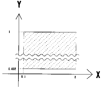
Referring to Figure 1, a range of 0.002-1 wt% nickel and a range of 0.1-2
wt% copper result in a good solder joint. When the base alloy is Sn-Cu, the
content of copper represented by the X axis is limited to a constant value
within a
range of 0.1-2 wt%. If the content of nickel is varied within a range of 0.002-
1
wt% with the copper content limited to within a range of 0.1-2 wt%, a good
solder
alloy is obtained. When the base alloy is Sn-Ni, the content of nickel
represented
by the Y axis is limited to a constant value within a range of 0.002-1 wt%. If
the
content of copper is varied within a range of 0.1-2 wt%, a good solder alloy
is
obtained. These ranges remain unchanged even if an unavoidable impurity,
which obstructs the function of nickel, is mixed in the alloy.
germanium has a melting point of .936°C, and dissolves in only a trace
amount into the Sn-Cu alloy. Germanium makes the crystal finer when the alloy
solidifies. Germanium appears on a grain boundary, preventing the crystal from
becoming coarse. The addition of germanium prevents oxide compounds from
developing during the solution process of the alloy. However, the addition of
germanium in excess of 1 wt% not only costs much, but also makes an
oversaturation state, hindering the molten alloy from spreading uniformly.
Excess germanium above the limit does more harm than good. For this reason,
CA 02288817 1999-11-08
the upper limit of the content of germanium is thus determined.
BRIEF DESCRIPTION OF THE DRAWING
Figure 1 is a graph showing proper ranges of additive metals.
DESCRIPTION OF THE PREFERRED EMBODIMENTS
The physical properties of solder alloys having the composition of the
present invention are listed in Table. The alloy of 0.6 wt% Cu, 0.1 wt% Ni,
and the
remaining percent Sn, which the inventors consider one of the proper
compositions
of solder alloy, was prepared.
Melting point:
Its liquidus temperature was approximately 227°C and its solidus
temperature was approximately 227°C. Tests were conducted using a
differential
thermal analyzer at a temperature rise rate of 20°C/minute.
Specific gravity:
The specific gravity of the alloy, measured using a specific gravity meter,
was approximately 7.4.
Tensile test under a 25°C room temperature atmosphere:
The tensile strength of the alloy was 3.3 kgf/mm2 with a stretch of
approximately 48%. The conventional Sn-Pb eutectic solder alloy, tested under
almost the same conditions, exhibited a strength of 4-S kgf/mm2. The alloy of
the
present invention has a tensile strength lower than that of the conventional
solder
alloy. However, considering that the solder alloy of the present invention is
CA 02288817 1999-11-08
6
chiefly intended to solder relatively light-weight electronic components onto
a
printed circuit board, the solder alloy of the present invention meets
strength
requirement as long as the application is limited to this field.
Spreading test:
The alloy, measured under JIS (Japanese Industrial Standards) 23197 Test
Standard, exhibited 77.6% at 240°C, 81.6% at 260°C, and
83.0% at 280°C.
Compared with the conventional tin-lead eutectic solder, the solder alloy of
the
present invention offers a small spreading factor, but is still sufficiently
acceptable.
Wettability test:
A copper strip of 7 x 20 x 0.3 mm was subjected to acid cleaning using
2% diluted hydrochloric acid and was tested for wettability under the
conditions of
a dipping rate of 15 mm/second, a dip depth of 4 mm, and a dipping time of S
seconds, using a wettability test apparatus. The zero crossing time and
maximum
wetting force of the alloy were 1.51 seconds and 0.27 N/m at 240°C,
0.93 second
and 0.3 N/m at 250°C, 0.58 second and 0.33 N/m at 260°C, and
0.43 second and
0.33 N/m at 270°C. From these results, the start of wetting is late at
higher
melting points, compared with the eutectic solder, but the wetting speed
increases
as the temperature rises. Since the metals to be soldered have typically low
heat
capacity in practice, the delay of the start of wetting presents no problem.
Peel test:
QFP lead peel tests showed a peel strength of approximately 0.9 kgf/pin.
A visual check to the peeled portion revealed that all peelings took place
between
a board and a copper land. This showed that the solder joint had a sufficient
CA 02288817 1999-11-08
7
strength.
Electric resistance test:
A wire solder of 0.8 mm diameter and 1 meter long was measured using
the four-terminal measurement method. Its resistance was 0.13 ,u SZ . The
resistance of the wire solder was close to that of tin. A low resistance
increases
the velocity of propagation of electrons, improving high-frequency
characteristics,
and changing acoustic characteristics. Measured under the same conditions, a
tin-lead eutectic solder alloy had an electric resistances of 0.17 !~ S2 and a
tin-
silver-copper solder had an electric resistance of 0.15 ,u SZ .
Creep strength test:
A tin-plated brass pin having a 0.8 x 0.8 mm square cross section was
flow-soldered onto a land of a 3 mm diameter with a hole of a diameter of 1 mm
formed on a paper phenolic board. A weight of 1 kg was hung on the pin using a
stainless steel wire in a temperature-controlled bath until the pin dropped
out of the
solder joint. With the bath temperature at 145°C, the pin remained
connected
over 300 hours. At 180°C, the pin did not fall even after 300 hours had
passed.
The pin connected by the tin-lead eutectic solder joint dropped within several
minutes to several hours under the same conditions. Different from the Pb
including solder, the solder alloy of the present invention has resistance to
creep
even if its tensile strength is low, and the reliability of the solder alloy
of the
present invention is particularly excellent under the high-temperature
atmosphere.
Heat shock test:
An hour of heat shock at -40°C and +80°C was given to the
solder alloy.
CA 02288817 1999-11-08
8
The solder alloy withstood 1000 cycles of shocks. The conventional tin-lead
eutectic solder alloy withstood S00-600 cycles of shocks.
Migration test:
A type II comb-like test specimen specified JIS Standard was dip-soldered
using RMA flux. Flux residues are cleaned, and resistance was measured with a
terminal attached to a lead wire. This measurement result was treated as an
initial
value. The test specimen was introduced into a thermohygrostat, and rated
direct
currents were applied for 1000 hours to measure resistance at predetermined
time
intervals while the test specimen was observed using a magnifier with a
magnification of 20 times. No abnormal change was observed both when 100
VDC current was applied at 40°C and a humidity of 95% and when 50
VDC
current was applied at 85°C and a humidity of 85%. This means that the
alloy of
the present invention performed as well as the conventional tin-lead eutectic
solder.
Leaching test:
A copper wire of 0.18 mm diameter with RA type flux attached thereto
was dipped in a solder bath filled with molten solder at 260~2°C. The
copper
wire was agitated until it disappeared by leaching, and the time to the full
leaching
was counted using a stopwatch. The full leaching of the copper wire in the
solder
of the present invention took about 2 minutes while the identical copper wire
leached in the tin-lead eutectic solder for about 1 minute. It is apparent
that the
longer resistance to the leaching was attributed to the addition of an
adequate
amount of copper. Specifically, the originally added copper that had leached
resulted a relatively slow copper leaching rate regardless of a large content
of tin.
CA 02288817 1999-11-08
9
Another likely reason for the slow leaching rate was that the melting point of
the
solder was higher than the eutectic solder by approximately 40°C.
The melting point and strength of the alloy having another composition is
listed in Table.
Studying the above tests results, compared with a comparative example,
all examples of the present invention present satisfactory results. The
conventional tin-lead eutectic solder alloy, measured under the same
conditions,
exhibited a strength of 4-5 kgf/mm2. All examples exhibited strength values
lower than that of the conventional tin-lead eutectic solder alloy. As already
described, the solder alloy of the present invention is chiefly intended to
solder
relatively light-weight electronic components onto a printed circuit board,
and the
solder alloy of the present invention meets strength requirement as long as
the
application is limited to this field.
No particular data were taken about the spreading of the samples. The
addition of nickel imparted a smooth surface structure to the alloy itself.
Since
the smooth surface was maintained after solidification, the spreading was
considered good.
The melting point are represented by two temperatures, in which a lower
one is a solidus temperature while a higher one is a liquidus temperature. The
smaller the temperature difference between the two, the less a component to be
soldered moves during solder solidification prior to the soldering operation,
and
the stabler the solder joint. This is also true of the conventional tin-lead
solder.
However, which solder outperforms which is not generally determined.
Depending on the application of solder, a solder alloy having an adequate
temperature difference may be employed.
CA 02288817 1999-11-08
Wettability to the copper, one of the important characteristics of solder, is
good with the RMA type flux. A good wettability is thus assured using the RMA
type flux.
The three-element Sn-Cu-Ni solder of the present invention may be
5 progressively formed by preparing the Sn-Ni base alloy and mixing a molten
Sn-
Cu solder with the base alloy for uniform diffusion. As already described, the
melting point of nickel is high. When pure nickel is introduced into the Sn-Cu
alloy, dissolving and diffusing nickel uniformly is difficult. To prepare the
alloy
of the present invention, the base alloy is beforehand melted at a relatively
high
10 temperature so that nickel is sufficiently mixed with tin, and the base
alloy is then
introduced into the molten Sn-Cu bath. In this way, the lead-free solder alloy
in
which nickel is diffused into tin at a relatively low temperature is obtained.
Forming beforehand the Sn-Ni base alloy helps prevent other unwanted
metals from being included thereinto. The present invention takes advantage of
the fact that nickel is in an all-ratio solid soluble relationship with copper
and that
the alloy of copper and nickel controls the development of bridges. The
presence
of any metal in the alloy that hinders the function of nickel is not
preferred. In
other words, the addition of any metal other than copper, which may easily
cooperate with nickel is not preferred in the present invention.
Although the lead-free solder of the present invention suffers a slow start
of wetting because of a melting point higher than that of the conventional tin-
lead
eutectic solder, the lead-free solder of the present invention forms an
interfacial
alloy layer quickly and reliably in accordance with a variety of surface
processes
once the wetting starts. The lead-free solder alloy of the present invention
has a
creep strength high enough to support bulky and heavy components and heat-
generating components. Since the copper leaching, which is considered serious
CA 02288817 1999-11-08
11
in the conventional solder alloy, is alleviated, the durability of lead wires
is
substantially increased.
Because of its high electric and thermal conductivities, the lead-free solder
of the present invention imparts high-speed property and high heat dissipation
property to electric components, and improves acoustic characteristics of
electric
components.
Since the lead-free solder of the present invention does not include, in its
composition, bismuth, zinc, and indium, it is free from an abnormal reaction
with a
coating containing lead that is soluble from a terminal materials, other lead-
free
solder coating such as Sn-Ag solder, Sn-Bi solder, and Sn-Cu solder. This
means
that the continuous use of a solder bath is assured and lead-rich wires
compatible
with lead are used without any problem when the conventional tin-lead solder
is
switched to the lead-free solder alloy of the present invention.
CA 02288817 1999-11-08
~"~etM et ~ N ~ M M N N
r
N
x
0
~t~hu'!,M, eh,eh,'MN M ~ .-
M M M M M M M M M CO
N
r~
C
~O N N M r- .-tl711~tp<p N
a U M M M M M etM ChM M M
N N N N N N N N N N N
0G \ \ \ \ \ \ \ \ \
\ \
~ ~ N ~ O ~ N 1~1'~1~N N N
i N ~ ~ ~ N ~ ~ ~
N N N
N ~-M
C
O
O
O
C
C~
~ O O O O W
O O
_ O O O O O O J
Z m
Q
H-
lly1i~t1'!f0 I~N 1i~47In 1!!1~
O O O O O O O O O C
7
U
c_c_c c c c c c c c c
cveow ~o co_ ~co~cv'~o 'cv'co
~9
n
N L ~ ~
L L L L L L L
0
U
- N M ~ !~c~~ o0O! j Q G7
L r
t0 p.
o
a c
o
o ~
U