Note: Descriptions are shown in the official language in which they were submitted.
CA 02288907 1999-10-22
WO 98/48525 PCTISE98/00722
AN ARRANGEMENT IN A SUBSCRIBER LINE INTERFACE CIRCUIT
TECHNICAL FIELD
The invention relates generally to subscriber line interface circuits and,
more
specifically, to an awangement for determining the line voltage in a
subscriber line
interface circuit.
BACKGROUND OF THE INVENTION
To be able to adjust hybrid interface parameters and gain in a telephone
circuit by
means of a microprocessor on a line interface board in order to obtain good
echo
cancellation for telephone lines of different lengths as well as for certain
test
purposes, it is necessary to know the length of the respective telephone line.
One way of estimating the length of the line is to measure the line voltage.
i.e. the
l~ voltage that appears across the line and the telephone set when a
connection is
established.
It is known to generate a pulse having a length corresponding to the line
voltage. To
get information about the line voltage, the length of this pulse is then
measured by
the microprocessor on the line interface board.
When a pulse length is to be measured, it is difficult to get at good
resolution since
the measurement period will be determined by the pulse length. The instruction
cycle of the microprocessor has to be short relative to the shortest pulse
length of
interest and, moreover, the microprocessor cannot do anything else during that
time.
SUMMARY OF THE INVENTION
The object of the invention is to bring about an arrangement in a subscriber
line
interface circuit for generating a signal for determining the line voltage
without
occupying the microprocessor unnecessarily.
CA 02288907 1999-10-22
WO 98/48525 PCT/SE98/00722
7
This is attained by means of the an-angement in accordance with the invention
in
that a sawtooth wave having an amplitude corresponding to the difference
between a
first and a second voltage, e.g. the voltages of the A-wire and the B-wire,
respectively, is ~~enerated and, in its turn, converted to a pulse train
related to the
line voltage.
In accordance with the invention, the pulse train is related to the line
voltage by its
pulse repetiton frequency and/or by its mark-space ratio. Depending upon the
actual
application, these different relationships offer different advantages.
Generally, by
generating a continuous pulse train and measul-ing its pulse repetition
frequency
and/or its mark-space ratio, it will be possible to freely choose the
measurement
period. Thus, a greater flexibility is obtained in accordance with the
invention.
BRIEF DESCRIPTION OF THE DRAWING
The invention will be described more in detail below with reference to the
appended
drawing, on which
Fig. 1 schematically illustrates a first embodiment of an arrangement
according to
the invention,
Figs. lA and 1B illustrate signals appearing in the embodiment according to
Fig. 1,
Fig. 2 schematically illustrates a second embodiment of an arrangement
according
to the invention, based on the awangement illustrated in Fig. 1,
Figs. 2A, 2B, ZC and 2D illustrate signals appearing in the embodiment
illustrated
in Fig. 2,
Fig. 3 schematically illustrates a third embodiment of an arrangement
according to
the invention, and
Figs. 3A and 3B illustrate signals appearing in the embodiment according to
Fig. 3.
PREFERRED EMBODIMENTS
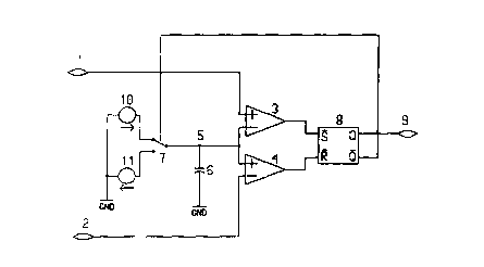
Fig. 1 illustrates a first embodiment of an arrangement according to the
invention
for generating a signal for determining the line voltage in a subscriber line
interface
~ .t
CA 02288907 1999-10-22
WO 98/48525 PCTISE98/00722
J
circuit connected to a telephone line having a high potential wire and a low
potential
were.
In the alTangement in Fig. l, the high potential wire or A-wire (not shown) is
~ 5 connected to a terminal 1, while the low potential wire or B-wire is
connected to a
terminal 2.
The terminal I is connected to the (+)-input terminal of a comparator 3, while
the
terminal 2 is connected to the (-)-input terminal of a comparator 4. The (-)-
input
terminal of the comparator 3 and the (+)-input terminal of the comparator 4
are
interconnected and the interconnection point is connected to a node 5. A
capacitor 5
is interconnected between the node 5 and ground GND.
The switching element of a voltage-controlled switch 7 is connected to the
node ~
and controlled to switch between its upper and lower position by means of a
signal
from the output terminal 0 of a bistable circuit 8 whose output terminal O
constitutes the output terminal 9 of the arrangement shown in Fig. 1. The
output
terminal 9 may be connected to a microprocessor (not shown), common to a
plurality of subscriber line interface circuits.
The inverted set input terminal S of the bistable circuit 8 is connected to
the output
terminal of the comparator 3, while the inverted reset input terminal R of the
bistable circuit 8 is connected to the output tel~ninal of the comparator 4.
In its upper position, as illustrated in Fig. 1, the switching element of the
switch 7
connects a first current generator 10 to the node 5 for charging the capacitor
6 as
indicated by an alTOw, while in its lower position, the switching element of
the
~ switch 7 connects a second current generator 11 to the node 5 for
discharging the
capacitor 6 as indicated by an arrow. The current generators 10 and I I are
interconnected between ground GND and the upper and lower terminals,
CA 02288907 1999-10-22
WO 98/48525 PCT/SE98100722
4
respectively, of the switch 7. The cuwent generators 10 and 11 may generate
currents of identical or different values.
The operation of the embodiment illustrated in Fig. 1 will now be described.
Suppose that the voltage across the capacitor 6, i.e. in the node 5, is of a
value
between the voltage V 1 on the A-wire connected to the terminal 1 and the
voltage
V2 on the B-wire connected to the terminal 2.
Under this condition, the output signal from the comparator 3 as well as from
the
comparator 4 will be a logic "1". These signals will not affect the bistable
circuit 8.
The bistable circuit 8 is supposed to have a logic "1" on its output terminal
Q and a
logic "0" on its invel-ting output O . The switching element of the switch 7
will then
be in its lower position (not shown) in which the cuwent from the current
generator
11 will discharge the capacitor 7 at a constant rate.
When the voltage across the capacitor 6, i.e. the voltage in the node 5, goes
below
the voltage on the B-wire connected to the terminal 2, the output signal from
the
comparator 4 will switch to a logic "0" which will reset the bistable circuit
8. Then,
the output O will go low,while the output O goes high. This causes the
switching
element of the switch 7 to switch to its upper position, connecting the
current
generator 10 to the node 5.
Now, the capacitor 6 will be charged at a constant rate until its voltage
exceeds the
voltage on the A-wire connected to the terminal 1. Then the comparator 3 will
switch its output signal, setting the bistable circuit 8 which again via the
switch 7
connects the current generator 11 to the node ~.
This operating cycle is repeated as long as the connection is kept active.
~ . i , t
CA 02288907 1999-10-22
WO 98148525 PCT/SE98I00722
Consequently, the voltage in the node ~ will be a sawtooth wave as illustrated
in
Fig. lA, while the output signal on the output terminal 9 will be a square-
wave
pulse train as illustrated in Fig. 1B.
The amplitude of the sawtooth wave shown in Fig. lA will be equal to the line
voltage, i.e. the voltage V 1-V2 between the input terminals 1 and 2.
The capacitance of the capacitor 6 as well as the values of the constant
currents
supplied by the current generators 10 and 1 l, are known. Since the capacitor
6 is
charged and discharged, respectively, by these constant currents between
voltages
depending on the line voltage, the line voltage can easily be deternvned from
the
pulse repetition fi-equency of the pulse train in Fig. 1B by means of the
microprocessor connected to the ourput terminal 9. The pulse repetition
frequency
of the pulse train on the terminal 9, as illustrated in Fig. 1B, will be
inversely
1S proportional to the line voltage.
A monostable circuit (not shown) may be connected to the output terminal 9 to
convert the pulses of the pulse train to pulses of equal width.
The advantage of such an embodiment is that it will be possible to extract
line
length information in two different ways:
On the one hand, as before, the pulse repetition frequency will be inversely
proportional to the line voltage.
On the other hand, the mean value of the output voltage will be inversely
proportional to the line voltage. The mean value is easily extracted by
lowpass
filtering.
Thus, such an embodiment gives an output signal that can be read directly by
the
microprocessor as a frequency or by an analog-to-digital converter.
CA 02288907 1999-10-22
WO 98/48525 PCT/SE98/00722
6
The operation of a second embodiment of the awangement according to the
invention will now be described with reference to Fig. 2.
The embodiment according to Fig. 2 resembles to some extent the embodiment as
shown in Fig. 1 as will be apparent from the below description.
In the embodiment according to Fig. 2, a capacitor I2 corresponding to the
capacitor
6 in Fig. 1, is charged and discharged between a first reference voltage VREF
1
applied to an input terminal 13, and a second reference voltage VREF2 applied
to a
input terminal 14. The terrninai 13 is connected to the (+)-input terminal of
a
comparator I5, while the terminal l4 is connected to the (-)-input terminal of
a
comparator 16 colesponding to the comparators 3 and 4, respectively, in Fig.
1.
The (-)-input terminal of the comparator 5 and the (+)-input terminal of the
comparator 16 are interconnected and the interconnection point is connected to
a
node 17. The capacitor 12 is interconnected between the node 17 and ground
GND.
The node 17 is also connected to the switching element of a voltage-controlled
switch 18 which as in the embodiment in Fig. I, is controlled between its
upper and
lower position from the output terminal D of a bistable circuit 19. In this
embodiment, the output terminal Q of the bistable circuit,19 is not used.
In the same manner as in the embodiment in Fig. 1, the input terniinals S and
R of
2~ the bistable circuit 19 are connected to the output terminals of the
comparators 15
and I6, respectively.
In its upper position, the switching element of the switch 18 connects a first
current
generator 20 to the node 17 for charging the capacitor 12 as indicated by an
arrow,
while in its lower position, the switching element of the switch I8 connects a
.__.. ..w~......~....~....~..~-_.... ~ ~ . r
CA 02288907 1999-10-22
WO 98148525 PCT/SE98100722
7
second current generator 21 to the node 17 for discharging the capacitor 12 as
indicated by an arrow.
Thus, the capacitor 12 will be charged and discharged between the voltages
VREF1
and VREF2, respectively, as illustrated in Fig. 2A where the upper line
corresponds
to the VREF 1 and the lower line corresponds to the voltage VREF2 as
indicated.
In the embodiment according to Fig. 2, the high potential wire, i.e. the A-
wire, of
the telephone line is supposed to be connected to a terminal 22, while the low
potential wire, i.e. the B-wire, is supposed to be connected to a terminal 23.
The terminal 22 is connected to the {+)-input terminal of a comparator 24,
while the
terminal 23 is connected to the (-)-input terminal of a comparator 25. The (-)-
input
terminal of the comparator 24 and the (+)-input terminal of the comparator 25
are
interconnected and the interconnection point is connected to the node 17.
The output terminal 26 of the comparator 24 and the output terminal 27 of the
comparator 25 are connected to the respective input terminals of an NAND-
circuit
28 whose output terminal constitutes the output terminal 29 of the embodiment
in
accordance with Fig. 2.
In Fig. 2A, the voltage on the A-wire connected to the terminal 22 is denoted
V22,
while the voltage on the B-wire connected to the terminal 23, is denoted V23.
As apparent from Fig. 2B illustrating the output signal from the comparator
24, the
output voltage V26 of the comparator 24 will be Iow when the voltage across
the
capacitor I2 exceeds the A-wire voltage V22, and high when the capacitor 12
voltage is below the A-wire voltage V22.
CA 02288907 1999-10-22
WO 98/48525 PCT/SE98100722
8
The output voltage V27 of the comparator 2~ as illustrated in Fig. 2C will be
high
as long as the voltage across the capacitor 12 is above the B-wire voltage
V23, and
low as long as the voltage across the capacitor 12 is below the B-wire voltage
V23.
Supplying the signals V26 and V27 to the input terminals of the NAND circuit
28
will result in an output signal from the NAND circuit 28 as illustrated in
Fig. 2D.
This output signal, denoted V29, will appear on the output terminal 29 of the
alTangement in Fig. 2.
As apparent, the pulse tz-ain appearing on the output tei~rninal 29 will have
a fixed
pulse repetition frequency. This is due to the fact that the capacitor 12 is
charged
and discharged between two constant voltages VREF l and VREF2 by means of
constant currents. The mark-space ratio of the pulse train will be
proportional to the
ratio between the line voltage and the difference between the reference
voltages
VREFI and VREF2 applied to the terminals 13 and 14, respectively.
The advantage of the embodiment according to Fig. 2 is that the mean value of
the
output pulse train voltage will be proportional to the line voltage if VREF 1
and
VREF2 are fixed. This mean value is easily extracted by means of Iowpass
filtering.
In applications including an analog-to-digital converter, this embodiment may
be
preferable.
Thus, also in this second embodiment, a pulse train related to the line
voltage will
be generated.
Fig. 3 illustrates a third embodiment of the invention.
In the embodiment according t~ Fig. 3, a capacitor 30 is charged and
discharged
between reference voltages VREF3 and VREF4. The reference voltage VREF3 is
applied to an input terminal 31, while the reference voltage VREF4 is applied
to an
~ ~ . T
CA 02288907 1999-10-22
WO 98148525 PCTISE98/00722
9
input terminal 32. The terminal 31 is connected to the (+)-input temninal of a
comparator 33, while the terminal 32 is connected to the {-)-input terminal of
a
comparator 34.
The (=)-input terminal of the comparator 33 and the (+)-input terminal of the
comparator 34 are interconnected and the interconnection point is connected to
a
node 3~. The capacitor 30 is interconnected between the node 35 and ground
GND.
The node 3~ is also connected to the switching element of a voltage-controlled
switch 36 which as in the embodiment in Fig. I, is controlled between its
upper and
lower position from the output terninal O of a bistable circuit 37 whose
output
terminal Q constitutes the output terminal 38 of the arrangement shown in Fig.
3.
In the same manner as in the embodiment in Fig. 1, the input terminals S and R
of
the bistable circuit 37 are connected to the output terminals of the
comparators 33
and 34, respectively.
In its upper position, the switching element of the switch 3u connects a first
current
generator 39 to the node 36 for charging the capacitor 30 as indicated by an
arrow,
while in its lower position, the switching element of the switch 36 connects a
second current generator 40 to the node 30 for discharging the capacitor 30 as
indicated by an arrow.
In the embodiment according to Fig. 3, the high potential wire, i.e. the A-
wire, of
the telephone line is supposed to be connected to a terminal 4I, while the low
potential wire, i.e. the B-wire, is supposed to be connected to a terminal 42.
The terminals 41 and 42, i.e. the A-wire and the B-wire, are connected to
control
input terminals 43 and 44 of the current generators 39 and 40 to control thzse
current generators to generate cuz-rents in response to the line voltage, i.e.
the
voltage between the terminals 41 and 42 or the A-wire and the B-wire.
CA 02288907 1999-10-22
WO 98148525 PCTlSE98/00722
Thus, the capacitor 30 will be charged and discharged between the constant
voltages
VREF3 and VREF4, respectively, as illustrated in Fig. 3A, by means of currents
that are proportional to the line voltage.
5
The resulting pulse train appearing on the output terminal 38, as illustrated
in Fig.
3B, will have a pulse repetition frequency which is proportional to the line
voltage.
As above, a monostable circuit may be connected to the output terminal 3 8 to
10 convert the pulses of the pulse train to pulses of equal width. Thus, the
output signal
will contain information about the line voltage both in its pulse repetition
frequency
and its mean value.
....._ . .._ _~._~ ~. ~ i , ~ .._.d..