Language selection

Search

Patent 2289201 Summary

Third-party information liability

Some of the information on this Web page has been provided by external sources. The Government of Canada is not responsible for the accuracy, reliability or currency of the information supplied by external sources. Users wishing to rely upon this information should consult directly with the source of the information. Content provided by external sources is not subject to official languages, privacy and accessibility requirements.

Claims and Abstract availability

Any discrepancies in the text and image of the Claims and Abstract are due to differing posting times. Text of the Claims and Abstract are posted:

  • At the time the application is open to public inspection;
  • At the time of issue of the patent (grant).
(12) Patent: (11) CA 2289201
(54) English Title: PHOTONIC CRYSTAL-BASED INTEGRATED OPTICAL CIRCUIT
(54) French Title: CIRCUIT OPTIQUE INTEGRE A BASE DE CRISTAL PHOTONIQUE
Status: Expired and beyond the Period of Reversal
Bibliographic Data
(51) International Patent Classification (IPC):
  • G02B 06/12 (2006.01)
  • G02B 06/122 (2006.01)
  • G02B 06/124 (2006.01)
  • G02F 01/01 (2006.01)
  • G02F 01/21 (2006.01)
  • G02F 01/225 (2006.01)
(72) Inventors :
  • KOOPS, HANS WILFRIED PETER (Germany)
  • DULTZ, WOLFGANG (Germany)
(73) Owners :
  • DEUTSCHE TELEKOM AG
(71) Applicants :
  • DEUTSCHE TELEKOM AG (Germany)
(74) Agent: SMART & BIGGAR LP
(74) Associate agent:
(45) Issued: 2006-10-03
(86) PCT Filing Date: 1998-04-29
(87) Open to Public Inspection: 1998-11-26
Examination requested: 2002-08-29
Availability of licence: N/A
Dedicated to the Public: N/A
(25) Language of filing: English

Patent Cooperation Treaty (PCT): Yes
(86) PCT Filing Number: PCT/EP1998/002532
(87) International Publication Number: EP1998002532
(85) National Entry: 1999-11-03

(30) Application Priority Data:
Application No. Country/Territory Date
197 20 784.7 (Germany) 1997-05-17

Abstracts

English Abstract


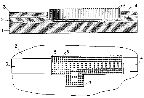
The invention relates to an integrated optical circuit comprising a silicon
substrate (1) and waveguides (2, 3) arranged thereon. At
least one photonic crystal is provided as a waveguide, which is formed by a
mesh of needles (6). The needles (6) can be produced by
corpuscular radiation deposition.


French Abstract

L'invention concerne un circuit optique intégré comportant un substrat de silicium (1) sur lequel sont disposés des guides d'ondes (2, 3). Au moins un cristal photonique faisant office de guide d'ondes est formé d'un réseau d'aiguilles (6), lesquelles peuvent être produites par dépôt par rayonnement corpusculaire.

Claims

Note: Claims are shown in the official language in which they were submitted.


CLAIMS:
1. Integrated optical circuit with a silicon
substrate and thereon disposed waveguides having at least
one photonic crystal, characterized in that elements (14),
which are each formed by a needle or a bore and which form
the photonic crystal, stand obliquely with respect to the
optical axis and are arranged parallel to one another.
2. Integrated optical circuit according to claim 1,
characterized in that further waveguides are in the form of
strip waveguides (3, 4), an insulating layer (2) being
disposed between the strip waveguides (3, 4) and the silicon
substrate (1), and in that the photonic crystal extends from
a plane below a lower boundary surface of the waveguides
(3, 4) to beyond an upper boundary surface of the waveguides
(3, 4).
3. Integrated optical circuit according to any one of
claims 1 or 2, characterized in that the elements of the at
least one photonic crystal are needles (14) having a high
dielectric constant which are arranged in the form of a two-
dimensional periodic lattice.
4. Integrated optical circuit according to any one of
claims 1 or 2, characterized in that the elements of the at
least one photonic crystal are holes of a low dielectric
constant in a body having a high dielectric constant which
are arranged in the form of a two-dimensional periodic
lattice.
5. Integrated optical circuit according to claim 3,
characterized in that the needles (14) stand on the
insulating layer (2), which is less thick in the region of
the photonic crystal than under the waveguides (3, 4).
9

6. Integrated optical circuit according to claim 3,
characterized in that the needles stand on the silicon
substrate.
7. Integrated optical circuit according to any one of
claims 3, 5 or 6, characterized in that the spaces between
the needles are filled with non-linearly optical material
and in that the refractive index of the non-linearly optical
material is adjustable by means of a voltage applied to
field electrodes (46 to 49).
8. Integrated optical circuit according to any one of
claims 1 to 7, characterized in that the at least one
photonic crystal (26) constitutes, through the arrangement
of imperfections, a branch filter in which branched-off
light of a selected wavelength range escapes laterally.
9. Integrated optical circuit according to any one of
claims 1 to 8, characterized in that laterally escaping
light of different wavelength ranges is capable of being
focused on different locations of a parallel extending
photonic crystal.

Description

Note: Descriptions are shown in the official language in which they were submitted.


CA 02289201 2006-03-10
28030-50
The invention relates to an integrated optical
circuit with a silicon substrate and thereon disposed
waveguides.
Integrated optical circuits are required in
communications engineering for various purposes, such as for
the distribution, combining, spectral splitting or switching
of information-modulated flows of light. In addition, it is
also possible to realize other circuits with the aid of
optical structures, such as computer circuits.
At present, integrated optical circuits are
constructed using waveguides made of polymers or III-V
compound semiconductors which are structured by lithographic
processes.
Suitable as the optically active components of
such circuits are, inter alia, photonic crystals, which,
because of their small geometrical dimensions, require, in
order to develop their full effect, a waveguide pattern into
which they are inserted. Such waveguide patterns are
usually strip waveguides made of polymer or semiconductor
material.
These waveguide patterns can be produced in a
complementary structure which, through its form, prevents
the propagation of the photon pulses in the matter and,
through selectively built-in defects, allows propagation
into otherwise completely reflecting matter. In this
regard, there is not a step change in refractive index as in
the guiding of waves in optical waveguides formed by doping
or in the form of strip waveguides, but, in this case, for
the propagation of said waves, - theoretically existing -
forbidden bands limit the state solution of the
1

CA 02289201 2006-03-10
28030-50
eigensolutions desired for specific wavelengths. These
waveguides are described, for example, by Mekis A. et al in
Physical Review Letters, Volume 77, No. 18, p. 3787.
The object of the present invention is to indicate
an integrated optical circuit in which such waveguides are
used for various functions and which can be manufactured
with the requisite precision.
The object of the invention is achieved in that at
least one photonic crystal is provided as a waveguide. It
is preferably provided that further waveguides are in the
form of strip waveguides, an insulating layer being disposed
between the strip waveguides and the silicon substrate, and
that the photonic crystal extends from a plane below the
lower boundary surface of the waveguides to beyond the upper
boundary surface of the waveguides.
The commercially available material "silicon on
insulator", for example from the manufacturer SOITEC SA.,
Grenoble, France, can advantageously be used to manufacture
the circuit according to the invention. Said material has
good transmission properties for wavelengths of 1.55 Vim.
Silicon has in such waveguides a very high dielectric
constant of 12, which can also be used with the photonic
crystals. Special photonic crystals, inserted with very low
insertion loss at defined locations of the circuit,
guarantee the functioning of the circuit, for example as a
computing circuit, it being possible for the entire circuit
to be made very small. Thus, for example, 6 periods of the
lattice of the photonic crystals with a lattice spacing of
1/3 of the wavelength are sufficient to obtain an
attenuation of 35 dB.
2

CA 02289201 2006-03-10
28030-50
An advantageous embodiment of the circuit
according to the invention consists in that the at least one
photonic crystal is formed by needles with a high dielectric
constant in the form of a two-dimensional periodic lattice
with imperfections. It is, however, also perfectly possible
that the at least one photonic crystal is formed by a body
with a high dielectric constant with holes of low dielectric
constant in the form of a two-dimensional periodic lattice
with imperfections, this being described, for example, in
DE19533148 A1.
Depending on the specific requirements, it may be
provided that the needles stand on the insulating layer,
which is less thick in the region of the photonic crystal
than under the waveguides, or that the needles stand on the
silicon substrate.
An advantageous further development of the circuit
according to the invention consists in that the spaces
between the needles are filled with non-linearly optical
material and in that the refractive index of the non-
linearly optical material is adjustable by means of a
voltage applied to field electrodes. It is thus possible to
control, for example, the behavior of filters in the form of
integrated optical circuits; see also DE19542058 Al.
A further advantageous embodiment consists in that
the needles or holes stand obliquely with respect to the
optical axis. This allows the branching of light in a part
of the wavelength range into a further plane of the
integrated optical circuit. An alternative thereto is
provided by another embodiment of the invention in that the
at least one photonic crystal constitutes, through the
arrangement of the imperfections, a branch filter in which
3

CA 02289201 2006-03-10
28030-50
branched-off light of a selected wavelength range escapes
laterally. The laterally escaping light can be guided
further in various manners.
In another further development of the invention,
it is provided that laterally escaping light of different
wavelength ranges is capable of being focused on different
locations of a parallel extending photonic crystal. This
makes it possible in a simple manner to connect a plurality
of computing planes.
Hereinbelow, example embodiments of the invention
are described in greater detail with reference to the
drawings, in which:
Fig. 1 shows a cross section of a detail from a
circuit according to the invention;
Fig, 2 shows a top view of the detail represented
in Fig. 1;
Fig. 3 shows a top view of a part of a further
example embodiment;
Fig. 4 shows an example of the optical connection
of two planes of the integrated optical circuit;
Fig. 5 shows the schematic representation of an
example of the optical connection of a plurality of
computing planes in a circuit according to the invention;
and
Fig. 6 shows a Mach-Zehnder interferometer
realized with the circuit according to the invention.
4

CA 02289201 2006-03-10
28030-50
In the example embodiment shown in Fig. 1, a
silicon substrate 1 accommodates an insulating layer 2 of
silicon oxide to which are applied optical strip waveguides
3, 4 made of silicon. Situated between the waveguides 3, 4
is a photonic crystal 5 formed by a lattice of needles 6.
In the example embodiment, the needles 6 stand on
the insulating layer 2, which has a cavity in the region of
the photonic crystal 5. This, allied to the fact that the
needles protrude beyond the upper boundary plane of the
waveguides 3, 4, means that the field conducted in
peripheral regions outside of the waveguide is also covered
by the photonic crystal.
The needles 6 may be manufactured in known manner
by corpuscular-beam deposition. An associated process is
described, for example, in DE19533148 A1.
As was demonstrated in S.Y. Lin, G. Arjavalingam:
Optics Letters, Vol. 18, No. 19, 1666 (1990) with reference
to experiments with millimeter waves, just six periods of
the lattice with a lattice constant of one-third of the
wavelength are sufficient in order to obtain an attenuation
of 35 dB. Within the thus attenuated wavelength range, it
is possible, by means of selective imperfections, i.e. by
the omission of needles, to create wavelength ranges of
reduced attenuation. In the example embodiment shown in
Figs. 1 and 2, light of a plurality of wavelengths is guided
from waveguide 3 to waveguide 4, while light of a selected
wavelength escapes at a branch 7. The selected intervals of
the needles in the central region of the photonic crystal
represent merely an example of a precise configuration for
obtaining the desired filter characteristics.
5

CA 02289201 2006-03-10
28030-50
In the example embodiment shown in Fig. 3,
photonic crystals are provided not only for a filter, but
also for the inlet and outlets, the inlet 11 and the outlets
12, 13 being in the form of all-pass filters in that there
are no needles in the central region.
Fig. 4 shows an example embodiment in which the
needles 14 forming the photonic crystal are tilted. A
covering layer 15 is provided in selected regions, with the
result that light escapes there and is focused through
attached lenses 16 made preferably of polymer material into
entrance windows (not shown) of an above-lying plane. This
allows three-dimensional structures, such as in a computer
circuit. The lenses may be produced in known manner by
electron-beam lithography or using optical processes.
Fig. 5 shows a detail from a circuit according to
the invention in which a plurality of branches 21 to 25 are
formed by a photonic crystal 26, a lens 27 to 31 focusing
the light escaping from the branch onto entrance surfaces 32
to 36 disposed on further optical components 37, 38
extending next to the photonic crystal 26.
Fig. 6 shows an example embodiment in the form of
a Mach-Zehnder interferometer. All the components,
particularly waveguide, filter, mirror and beam splitter,
are formed by photonic crystals. The interferometer is to
be used to measure the transit time in a reflecting test
specimen 41 merely schematically indicated in Fig. 6. For
this purpose, the light supplied at directional filter 42 is
first guided through an adjustable filter 43, by means of
which the wavelength to be used for measuring is selected.
By means of a beam splitter 44, the light escaping from the
filter 43 is guided in equal parts straight ahead to an
6

CA 02289201 2006-03-10
28030-50
adjustable phase shifter 45 and reflected to the test
specimen 41.
The adjuster filter 43 and the adjustable phase
shifter 45 each consist of a photonic crystal, the spaces
being filled with non-linearly optical material, the
dielectric constant of which and thus the optically active
intervals of the needles are controllable by means of
voltages applied to electrodes 46, 47 and 48, 49.
The phase shifter 45 is adjoined by a completely
reflecting mirror 50, which supplies the light escaping from
the phase shifter 45 to a further beam splitter 51.
Disposed in front of the test specimen 41 is a
photonic crystal in the form of a directional filter 42,
with the effect that the light arriving from the beam
splitter 44 is guided into the test specimen 41 and the
light reflected in the test specimen passes through
adjustable filter 43 to the further beam splitter 51. Both
flows of light are superimposed at the output 52. Using a
suitable instrument transformer, the intensity escaping from
the output 52 can be measured and the phase shift in the
test specimen 41 can be determined by adjusting the phase at
45 to a minimum of the intensity at the output 52 for the
reasons already mentioned hereinbefore, it is also possible
for the circuit shown in Fig. 6 to be made extremely small,
for example with an overall length of approximately 20 Vim.
In accordance with this invention there is
provided an integrated optical circuit with a silicon
substrate and thereon disposed waveguides having at least
one photonic crystal, characterized in that elements (14),
7

CA 02289201 2006-03-10
28030-50
which are each formed by a needle or a bore and which form
the photonic crystal, stand obliquely with respect to the
optical axis and are arranged parallel to one another.
8

Representative Drawing
A single figure which represents the drawing illustrating the invention.
Administrative Status

2024-08-01:As part of the Next Generation Patents (NGP) transition, the Canadian Patents Database (CPD) now contains a more detailed Event History, which replicates the Event Log of our new back-office solution.

Please note that "Inactive:" events refers to events no longer in use in our new back-office solution.

For a clearer understanding of the status of the application/patent presented on this page, the site Disclaimer , as well as the definitions for Patent , Event History , Maintenance Fee  and Payment History  should be consulted.

Event History

Description Date
Time Limit for Reversal Expired 2010-04-29
Letter Sent 2009-04-29
Inactive: Late MF processed 2008-07-03
Letter Sent 2008-04-29
Grant by Issuance 2006-10-03
Inactive: Cover page published 2006-10-02
Pre-grant 2006-07-21
Inactive: Final fee received 2006-07-21
Notice of Allowance is Issued 2006-06-30
Letter Sent 2006-06-30
Notice of Allowance is Issued 2006-06-30
Inactive: Approved for allowance (AFA) 2006-04-11
Inactive: IPC from MCD 2006-03-12
Amendment Received - Voluntary Amendment 2006-03-10
Inactive: S.30(2) Rules - Examiner requisition 2005-09-26
Letter Sent 2002-10-25
Amendment Received - Voluntary Amendment 2002-09-18
Request for Examination Requirements Determined Compliant 2002-08-29
All Requirements for Examination Determined Compliant 2002-08-29
Request for Examination Received 2002-08-29
Letter Sent 2000-03-09
Inactive: Single transfer 2000-02-09
Inactive: Cover page published 2000-01-05
Inactive: IPC assigned 1999-12-24
Inactive: First IPC assigned 1999-12-24
Inactive: Courtesy letter - Evidence 1999-12-14
Inactive: Notice - National entry - No RFE 1999-12-09
Application Received - PCT 1999-12-07
Application Published (Open to Public Inspection) 1998-11-26

Abandonment History

There is no abandonment history.

Maintenance Fee

The last payment was received on 2006-03-22

Note : If the full payment has not been received on or before the date indicated, a further fee may be required which may be one of the following

  • the reinstatement fee;
  • the late payment fee; or
  • additional fee to reverse deemed expiry.

Patent fees are adjusted on the 1st of January every year. The amounts above are the current amounts if received by December 31 of the current year.
Please refer to the CIPO Patent Fees web page to see all current fee amounts.

Owners on Record

Note: Records showing the ownership history in alphabetical order.

Current Owners on Record
DEUTSCHE TELEKOM AG
Past Owners on Record
HANS WILFRIED PETER KOOPS
WOLFGANG DULTZ
Past Owners that do not appear in the "Owners on Record" listing will appear in other documentation within the application.
Documents

To view selected files, please enter reCAPTCHA code :


To view images, click a link in the Document Description column. To download the documents, select one or more checkboxes in the first column and then click the "Download Selected in PDF format (Zip Archive)" or the "Download Selected as Single PDF" button.

List of published and non-published patent-specific documents on the CPD .

If you have any difficulty accessing content, you can call the Client Service Centre at 1-866-997-1936 or send them an e-mail at CIPO Client Service Centre.


Document
Description 
Date
(yyyy-mm-dd) 
Number of pages   Size of Image (KB) 
Representative drawing 2000-01-04 1 22
Description 1999-11-02 3 221
Abstract 1999-11-02 1 60
Claims 1999-11-02 2 75
Drawings 1999-11-02 3 154
Drawings 2006-03-09 3 145
Description 2006-03-09 8 280
Claims 2006-03-09 2 65
Representative drawing 2006-09-05 1 35
Notice of National Entry 1999-12-08 1 193
Reminder of maintenance fee due 1999-12-29 1 113
Courtesy - Certificate of registration (related document(s)) 2000-03-08 1 113
Acknowledgement of Request for Examination 2002-10-24 1 176
Commissioner's Notice - Application Found Allowable 2006-06-29 1 161
Maintenance Fee Notice 2008-06-09 1 171
Late Payment Acknowledgement 2008-07-27 1 164
Maintenance Fee Notice 2009-06-09 1 171
Correspondence 1999-12-08 1 14
PCT 1999-11-02 14 516
PCT 1999-11-03 6 209
Correspondence 2006-07-20 1 38