Note: Descriptions are shown in the official language in which they were submitted.
CA 02289357 1999-11-10
DIGITAL SIGNAL TRANSMITTER AND RECEIVER USING SOURCE BASED
REFERENCE LOGIC LEVELS
FIELD OF THE INVENTION:
The present invention relates to a signal transmitter for
transmitting digital logic signals and a complementary receiver,
and more particularly to a digital logic transmitter that
generates one or more reference signals, to be used by the
receiver to establish threshold levels for digital HI and LO
signals.
BACKGROUND OF THE INVENTION:
Digital electronic systems typically utilize very large
scale integrated circuit ("VLSI") blocks. VLSI blocks, are
interconnected to each other within an electronic system by
electronic conductors that act as transmission lines. Digital HI
and LO signals are represented by two distinct voltage levels
presented on the conductors. A "driver" forming part of one VLSI
block couples a transmitting VLSI block to the transmission
lines. Similarly, a "receiver" forming part of a receiving VLSI
block, couples the receiving VLSI block to the lines. Each
driver and receiver typically comprises a plurality of
transistors formed on the respective VLSI blocks.
The transistors forming the drivers and receivers are
coupled to ground points on the VLSI blocks. These ground
points, however, are not at the same potential as the external
1
CA 02289357 1999-11-10
ground potential of the VLSI packages. Drivers are coupled to
the external ground connection through a package impedance. This
package impedance typically has resistive, inductive, and
capacitive components and is therefore a source of electrical
noise present when a driver output switches from LO to HI or HI
to LO. This noise is typically referred to as a "ground bounce".
At the receiver, binary HI and LO signals are typically
distinguished by their voltage levels relative to the receiver
package ground. Signals that exceed a threshold voltage level
represent a digital HI while signals that fall beneath another
threshold voltage represent a digital LO. As will be
appreciated, the presence of noise from the transitioning signal
at the transmitter, may cause a signal not intended to cross a
threshold to cross this threshold, as sensed at a receiver.
This, in turn, may lead to errors in the received signal.
Numerous digital drivers and receivers address this problem.
For example, the gunning transceiver logic ("GTL") family as more
particularly described in U.S. Patent No. 5,023,488 uses low
voltage swings that reduce transient effects of parasitic
impedances, including package impedances. As well, this patent
discloses clamping the drain to source of a GTL driver to reduce
the rate at which current is drawn so as to provide increased
damping for noise due to transient voltages.
Still other logic families use differential outputs. As the
effect of parasitic impedances is the same for both outputs of a
differential pair, differential signals naturally reject common
2
CA 02289357 1999-11-10
mode noise. Differential signals, however, require double the
number of outputs for a transmitting VLSI block; double the
number of transmission lines interconnecting the transmitting
VLSI block to the receiving VLSI block; and double the number of
inputs at the receiving VLSI block. As will be appreciated, it
would often be desirable to eliminate these extra inputs, outputs
and interconnects.
Accordingly, an alternative to known approaches to reduce
l0 the effects of package impedance in digital transmitters and
receivers is desirable.
SUMMARY OF THE INVENTION:
In accordance with the present invention a transmitter and
complementary receiver use HI and/or LO reference signals
generated at the transmitter, and transmitted to the receiver.
The reference signals are used at the receiver to account for
noise components in received signals that are representative of
digital HI or LO signals.
In accordance with an aspect of the invention, there is
provided a signal transmitter block formed as part of an
integrated circuit. The transmitter block transmits digital
signals to a receiver. The transmitter block includes several
signal drivers, each for generating output voltages at a signal
driver output, that when measured relative to a ground point on
the integrated circuit are representative of digital HI and LO
signals. A first reference driver, for generating at a first
3
CA 02289357 1999-11-10
reference output an output voltage that when measured relative to
the ground point, corresponds either a digital HI signal;
or a digital LO signal, forms part of the block. The first
reference driver and the signal drivers are electrically
interconnected to the ground point on the integrated circuit
block. The ground point is further interconnected through an
impedance on the integrated circuit block to a system ground
connection for the integrated circuit, so that current flowing
from and to the system ground connection through the ground point
to the signal drivers and the first reference driver flows
through the impedance.
In accordance with another aspect of the invention, a
digital signal receiver block having receiver block outputs for
generating digital HI and LO signals, includes several
comparators. Each comparator has a signal input for receiving a
voltage signal representative of one of a digital HI signal and
LO signal and a noise signal; an output interconnected with one
of the receiver block outputs; and a first reference input for
receiving a reference voltage signal including a signal
indicative of a digital LO signal, and a noise signal. The first
reference inputs of the several comparators are interconnected so
that each of the reference inputs receives the same reference
voltage signal. Each of the comparators is adapted to produce at
its output a signal representative of a digital LO signal when a
voltage at its signal input is less than a threshold voltage
derived from a reference voltage at its first reference input.
In accordance with yet another aspect of the present
4
CA 02289357 1999-11-10
invention, there is provided a method of transmitting and
receiving several signals representative of digital HI and LO
signals from a transmitter to a receiver. The method includes
the steps of a. concurrently transmitting the several signals,
each having a voltage level representative of one of a digital HI
and LO signal and a noise signal from a transmitter to a
receiver; b. transmitting a reference signal comprised of a
signal having a voltage level representative of a HI signal and a
noise signal to the receiver; c. receiving the several signals
and the reference signal at the receiver; d.comparing the
reference signal to each of the several signals; e. outputting a
signal representative of a digital HI signal at the receiver, for
each of the several signals that exceeds a threshold voltage
derived from the reference signal.
Advantageously, the invention provides rejection of noise
signals without the use of differential signals.
Other aspects and features of the present invention will
become apparent to those of ordinary skill in the art upon review
of the following description of specific embodiments of the
invention in conjunction with the accompanying figures.
BRIEF DESCRIPTION OF THE DRAWING:
In figures which illustrate, by way of example only,
embodiments of the present invention,
FIG. 1 is a schematic diagram of a digital transmitter block
5
CA 02289357 1999-11-10
exemplary of an embodiment of~the present invention;
FIG. 2 is a schematic diagram of a receiver block exemplary
of an embodiment of the present invention
FIG. 3 is a schematic diagram of a signal transmitter and
receiver system exemplary of an embodiment of the present
invention;
FIG. 4 illustrates a plurality of signal waveforms present
in the system of FIG.3, in operation; and
FIG. 5 illustrates a further plurality of signal waveforms,
present in the system of FIG. 3, in operation.
DETAILED DESCRIPTION:
FIG.1 schematically illustrates a signal transmitter block
10, exemplary of a preferred embodiment of the present invention.
Signal transmitter block 10 is formed as part of a VLSI block 11
in accordance with generally known VLSI design and fabrication
techniques.
Transmitter block 10 comprises a plurality of digital signal
drivers 12a to 12c (individually and collectively 12). For
clarity, only three signal drivers are illustrated. A person
skilled in the art will appreciate that a typical transmitter
(usually comprise) more than three drivers. Each driver has a
signal input 22 (22a to 22c for drivers 12a to 12c,
respectively); a clock input 20 (20a to 20c for drivers 12a to
12c, respectively); and an output 32 (32a to 32c for drivers 12a
to 12c, respectively). On the transition of a clock pulse at
clock input 20, a driver presents at its output 32 voltage levels
6
CA 02289357 1999-11-10
representative of digital HI and LO signals corresponding to an
input signal presented at its signal input 22.
Transmitter block 10 further comprises a reference HI driver
14 and reference LO driver 16, having signal inputs 26 and 30,
clock inputs 24 and 28, and outputs 34 and 36, respectively.
Like signal drivers 12, reference drivers 14 and 16 present at
their outputs 34 and 36 signals representative of their inputs 26
and 30 upon the transition of a clock signal at clock inputs 24
and 28.
Preferably, a common clock input 21, interconnects all clock
inputs 20 ,24 and 28 of drivers 12, 14 and 16.
All of the drivers 12, 14 and 16 are preferably formed of
identical electric components and typically comprise one or more
known transistor devices. Each driver may for example be a CMOS
or bi-polar driver providing transistor to transistor (TTL)
logic, positive emitter coupled logic (PECL), or other outputs.
A person skilled in the art will appreciate that other drivers
may be appropriately used. Reference drivers 14 and 16 are thus
typical drivers, of the same type used as signal drivers 12.
As illustrated, each driver 12, 14, 16 is connected to a
positive voltage source rail 17 interconnected through power
supply interconnection impedance Ztraaamitter~acxage~over supply 40 t0
external power supply voltage *V~~. Further, each driver is
connected to an on chip ground rail 37 (GND) formed as part of
VLSI block 11. VLSI block 11 is further connected to an external
7
CA 02289357 1999-11-10
system ground 60. Because of the package impedance of VLSI block
11 and system ground impedances unique to the transmitter ground
current path, ground rail 37, the ground connection point for
drivers 12, 14 and 16, is actually coupled to system ground 60
through an impedance that may modelled by an impedance
Ztranemitter_package_ground 38. The combination of impedances
Z'transmitter~ackage~ower supply 4 ~ and Ztranamitter_package_grouad 3 $
represent the
total package impedance of VLSI block 11. Power supply
interconnection impedance Ztreaemitter~ackage~OVer supply 40 and ground
impedance Ztreaamitter~ackage_ground 38 may be modelled as having
resistive, capacitive and inductive components. As will be
appreciated, it is possible that power supply interconnection
impedance Ztraamitter~ackage~over supply 40 and package impedance
Ztraasmitter~ackage_grouad 3 8 are non-1 inear .
Signal inputs 26 and 30 of reference drivers 14 and 16 are
interconnected with gates 23 and 25, respectively. The input of
gate 23 is connected to 'V~~ causing the output of gate 23 to
produce a voltage representative of a logic HI at input 26 of
driver 14. Similarly, the input of gate 25 is connected to
system ground 60 causing the output of gate 25 to produce a
voltage representative of a logic LO signal at input 30 to driver
16. As will become apparent, outputs 34 and 36 of drivers 14 and
16 thus always generate HI and LO output signals, used as
reference signals. Gates 23 and 25 need not be formed as part of
transmitter block 10.
Signal inputs 22 to drivers 12 may be interconnected to n
input signals, typically originating on VLSI block 11. These
8
CA 02289357 1999-11-10
input signals may, for example, ultimately emanate from n address
or data lines of an n bit computer bus. Typically, these n input
signals are synchronous and clocked by their source. Common
clock input 21 is thus typically interconnected to a system clock
which may also be provided by the clock of a computer.
FIG. 2 illustrates a receiver block generally marked 70
exemplary of a preferred embodiment of the present invention. In
the preferred embodiment, receiver block 70 is formed as part of
a VLSI block 72 that is physically distinct from VLSI block 11
(FIG. 1). VLSI block 72 is connected to system ground 90.
Receiver block 70 comprises a plurality of comparators 74a to 74c
(individually and collectively 74). For clarity, only three
comparators 74a to 74c are illustrated. A person skilled in the
art will appreciate that a typical receiver block comprises more
than three such comparators and typically one comparator for each
transmitter in a complementary transmitter block. Each
comparator 74 takes at its input 80 (80a to 80c for comparators
74a to 74c, respectively) a reference signal and an input signal
at input 78 (78a to 78c for comparators 74a to 74c,
respectively). Outputs 82 (82a to 82c for comparators 74a to
74c, respectively) present a fixed output voltage if an
associated input 78 is less than a trigger voltage derived from
the reference signal at reference input 80. Typically, the
trigger voltage equals the reference voltage plus a noise or
hysteresis margin, V""~;a. Comparators 74 may be designed to
allow for adjustment to the hysteresis margin, in accordance with
design techniques known to those skilled in the art.
9
CA 02289357 1999-11-10
As illustrated, each comparator 74 is connected to a
positive voltage source 'V~~, preferably interconnected with ~V~~
of VLSI block 11. Package and power supply interconnect
impedances of VLSI block 70 that might be modelled similar to
Ztransmitter~ackage grouad 38 and Ztraaamitter~ackage_pover supply 4~ of VLSI
blOCk 11
have been illustrated a8 Zreceiver~ackage_ground 66 and Zreceiver~ower supply
68.
Outputs 82 of comparators 74 are interconnected with
latching block 76. Latching block 76 further takes as an input a
clock signal presented at clock input 84. Latching block 76
latches at its outputs 86a to 86c (individually and collectively
86) logic input values 82a to 82c, respectively, upon sensing a
transition of clock input 84. Latching block 76 may for example
comprise a plurality of D-type flip-flops whose inputs are
connected to comparator outputs 82a to 82c and whose outputs
represent the latch outputs 86a to 86c. A person skilled in the
art will appreciate a variety of latching circuits that could be
used in place of the D-type flip flops. Typically, outputs 86
are interconnected with another functional circuit block (not
shown) of VLSI block 72, that may process signals presented at
outputs 86.
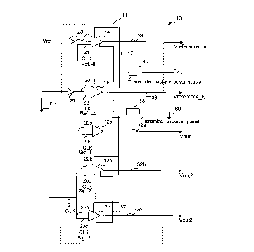
FIG. 3 illustrates an exemplary interconnection of
transmitter block 10 (FIG: 1) with receiver block 70 (FIG. 2)
forming a digital transmitter and receiver system generally
marked 92. As illustrated outputs 34 and 32a to 32c of
transmitter block 10 are interconnected with transmission lines
94, and 96a to 96c, respectively. Ground 60 is interconnected
CA 02289357 1999-11-10
with ground 90. These transmission lines are typically traces of
a printed circuit board interconnecting VLSI blocks 11 and 72.
Inputs 78a to 78c of receiver block 70 are interconnected
with the terminating ends of transmission lines 96a to 96c.
Additionally, transmission line 94 interconnected with reference
HI driver 14, is interconnected with reference input 80a (80 in
FIG. 3) of receiver block 70. As well, a common clock source is
interconnected with driver clock input 21 and receiver block
clock input 84. Of course, clock input 84 could be driven by a
signal otherwise derived and interrelated with a signal at clock
input 21. For example, VI,SI block 72 could comprise a phase
locked loop, locked to a clock signal on VLSI block 11 used to
clock receiver block 70. Alternatively, a clock signal may be
recovered from a data stream at receiver block 70.
In system 92, reference HI driver 14 and its output 34 are
not interconnected to receiver block 70. As will become
apparent, reference drivers 14 and 16 provide voltage levels
representative of digital reference HI and LO signals,
respectively. Only one of reference drivers 14 or 16 is
required. Thus, one of drivers 14 and 16 is optional and could
be eliminated. In practise, if only a single reference driver is
used, reference LO driver 14 is preferably used as "ground
bounce" noise more significantly affects logic LO signals, than
logic HI signals.
FIGS. 4 and 5 illustrate various signals present in the
system depicted in FIG. 3, in operation.
11
CA 02289357 1999-11-10
Specifically, FIG. 4 illustrates input signals present at
transmitter block 10 for two complete clock cycles 100 at clock
inputs 21 and 84 as shown in FIGS. 1-3.
In the operational example, voltage levels representing
digital HI and LO signals are represented by positive voltage
values ~V~~ for binary HI signals and .7~V~~ for binary LO signals,
both measured relative to system ground 60. The receiver is
designed to operate with a hysteresis or noise margin of .1+V~~.
Accordingly, a binary HI signal is therefore generated for inputs
greater than .9~V~~, while a binary LO signal is generated for
inputs less than .8~V~~. In other words, voltage signals
exceeding .9~V~~ are interpreted as digital HI signals, while
voltage signals less than .B~V~~ are interpreted as digital LO
signals. Of course, depending on the precise drivers,
transmitters and receivers exemplary of the present invention may
use other voltage levels, such as for example, typical CMOS or
TTL logic levels.
In the illustrated example, signals 106 and 108 are applied
to signal inputs 22a and 22b, of drivers 12a and 12b of
transmitter block 11 (FIGS. 1 and 3), respectively. As
illustrated input signal 106 represents a binary HI in both clock
cycles, while input signal 108 represents a binary HI signal in a
first clock cycle, followed by a transition to a binary LO in a
second clock cycle. For illustration, voltages representing
logic HI and LO values at inputs 22 are chosen as 'V~~ and . 7'V~~,
respectively. Of course, logic voltage levels at inputs 22 need
not be the related to output voltages or threshold voltages
12
CA 02289357 1999-11-10
presented at inputs 26 and 30. Transmitter block 10 could easily
be adapted to translate input logic levels to other output
values. Signals 100, 102, 104 and 106 are measured relative to
GND at rail 37, and are therefore free from noise due to the
package impedance Ztranamitter_package_ground 3 8 and Ztr~tter_package~over
supply
40 of VLSI block 11.
The outputs of transmitter block 10, at outputs 34, 36 and
32a and 32b (illustrated in FIG. 1) measured relative to system
ground 60, in operation, are depicted in FIG. 5. As well, for
convenience, clock signal 100 is again illustrated.
As illustrated, Vraference ni ~d Vreterance to deviate from the
expected ~Vcc and '~7Vcc because of the voltage drops across
Ztranamitter-package_grouad 3 a and Z transmitter~ackage-power supply 4 ~ .
Output reference signal Vratar~p~~ ni 110 measured relative to
system ground 60 at output 34 of driver 14 exhibits slight
ringing (not shown) at the commencement of each cycle of clock
signal 100. This ringing is attributable to transient current
through package impedance Ztransmitter~ackage_grouad 3 8 ~d
?'traasmitter~ackage~ower supply 40, and the resulting voltage signals. As
previously noted, Ztraaomitter~ackage_ground 38 and Ztranamitter~ackage_pover
supply
40 may be modelled as comprising resistive, inductive and
capacitive components. As illustrated, the duration of the
ringing is typically only a fraction of the clock period. The
duration and amplitude of the ringing is dependent on the values
Of ?'traaamitter~ackage_ground 3 8 and Ztranymitter_package~ower supply 4 ~ as
wel l a8
the amount and rate of current provided to drivers 12, 14 and 16.
13
CA 02289357 1999-11-10
More significantly, as illustrated, output reference signal
Vrefereace h~ e~ibits an upward voltage drift relative to system
ground 60 at the commencement of each clock cycle. This upward
drift is attributable largely to the Zpackagerpowez ~upply_ground 38
portion of the package impedance. Specifically, as reference hi
driver 14 produces its output relative to chip ground 37, and
~'package.power supply_ground 38 introduces a further voltage drop between
chip ground 37 and system ground 60, that manifests itself in the
illustrated upward drift or "ground bounce". As well, a voltage
drop in the HI signals may be attributable to the voltage drop
caused by current through Zt=,a,~tte=~~,~ge,~=_"mY 40. However,
Vreference h~ is affected by a similar drop.
It is worth noting that effect of V~o"~ no;,~ is far more
significant in sensing logic LO signals at the receiver. This
is because the upward voltage drift caused by the voltage drop
across Z~= ",~lY_gr~ causes LO signals to drift above the
threshold required by receiver 70 to detect a logic LO signal.
This same drift will cause HI signals that already exceed the
minimum voltage for a HI signal to merely further exceed this
signal.
As such, in practise, if only a single reference driver is
used, reference LO driver 14 is preferably used as "ground
bounce~~ noise more signifcantly affects logic LO signals than
logic HI signals.
14
CA 02289357 1999-11-10
A reference LO Slgnal Vreference_lo 112 at output 36 measured
relative to system ground 60 experiences similar drift and
ringing as do driver output signals Vo"il 114 and Va"tZ 116 at
outputs 32a and 32b of drivers 12a and 12b. As will be
appreciated, and as illustrated, neglecting any pin impedance,
the ringing and drift in signals 110, 112, 114 and 116
attributable to package impedance Ztraasmitter package_grouad 38 will be
substantially similar in all n drivers 12a to 12c as well as
reference LO and HI drivers 14 and 16 as they are connected to
system ground 60 through common package impedance
?'tranamitter~nckage_grouad 3 8
Similarly, the ringing and drift in signals 110, 112, 114
and 116 attributable to power supply interconnect impedance
ZS Ztranamitter~ackage~pover supply 40 will be identical, as current provided
by
an external power supply to all drivers 12a to 12c as well as
reference LO and HI drivers 14 and 16 must flow through common
power supply impedance Ziranamitter~ackage~over supply 40.
More specifically, the instantaneous output voltage of each
driver at outputs 32, 34 or 36 relative to system ground 60, may
be modelled as:
Vout n = Vdriver a + Vnoise.
where V~i"~r" is the output of the nth driver at transmitter 10,
measured relative to "chip" ground 37
Assuming that noise other than package ground and power supply
CA 02289357 1999-11-10
interconnect noise is negligible, and further assuming that
Vgrouad noise > > Vpover supply noise
Vout n-Vdriver n '~Vgrouad aoiae
Vground ao~ee~ may further be modelled as
Vground noioe -=ground package*Ztranemiter~ackage_grouadr
with
=ground package-=ground driver total -=ground driver 1'~I ground driver Z '*
ground driver a
+ I ground refdriver hi '* I ground refdriver to
Thus, the instantaneous contribution of vaoiae to each output
signal vo"ta is identical for each driver output signal.
Moreover, the contribution of vnoise depends on the total current
drawn by transmitter block 10, and therefore will vary from clock
cycle to clock cycle, depending on the number of drivers
producing HI or LO outputs.
Assuming pin and transmission line effects are negligible,
in FIG 3. signals at outputs 32a, and 32b of transmitter block 10
are presented at receiver inputs 78a and 78b through lines 96a
and 96b. Similarly, signal 112 of FIG. 4 at reference LO output
36 of transmitter block 10 is presented at reference LO input 80
interconnected with comparator reference inputs 80a and 80b of
FIG. 2 of receiver 70 through line 94.
16
CA 02289357 1999-11-10
At the receiver, the effect of current drawn by the
transmitter block 10 will have a negligible effect on receiver
block 72. However, as illustrated, voltage levels received at
the receiver block 72, measured relative to system ground 60 will
fluctuate, often significantly, depending largely on the current
drawn through Ztr~"~;~t~= acxa ~
~ 9 _Jrotmd 3 8 .
As will become apparent, use of comparators and reference
signals Vref~r~~~ ~i and Vr~ference_lo signals attempt to compensate for
such fluctuations.
Specifically the output 82 of each comparator 74 in FIG. 2,
varies depending on whether or not the voltage level of the input
signal at input 78 exceeds the reference voltage presented at
input 80 less a hysteresis margin. If it does, output 82 will
assume a voltage value representative of a digital HI signal at
its output and at the input latching block 76.
Voltages at comparator inputs 80 and 78 are measured
relative to each other. Output 82 is only LO if
Vcomparator n=Vout~Vreference_lo + Vein ~ Because the comparator inputs are
measured relative to each other, any common mode noise in the
driver and reference signal will be ignored. This is best
illustrated by considering signal Vreference_lo and Vout relative to
system ground 60.
Thus,
Vreference_lo=Vref+Vaoi~e, where Vr~f is the threshold voltage
measured relative to chip ground rail 37 and
17
CA 02289357 1999-11-10
Vcomperator n=Vout n=Vdriver a+Vnoise
As noted, this leads to a LO comparator output only when
Vcomparator n ~ Vreference_lo 'f Vmargia
Vdriver n + Vnoiae ~ Vref ~' Vnoiae +vmargia i Or
Vdriver n ~ Vref ~' Vmargin
1~
This precisely defines the required threshold level required
to generate a digital output LO signal. Thus, the parasitic
effects of source package impedance Ztraanmitterrpwckage_grouad 38 and
power supply interconnect impedance Ztraaimitter~ackage~rer supply 40, are
eliminated through the use of a reference signal provided by
driver 16 of transmitter block 10 to a receiver block 70
comprising a plurality of comparators 74.
In FIG. 2, on the rising edge of clock signal 100 of FIG. 4,
latching block 76 latches at its outputs 86 the outputs of
comparators 74. These outputs are typically provided to another
functional block (not illustrated) formed as part of vLSI block
72.
Provided that drivers 12, 14 and 16 are formed in geometric
proximity to each other, the effect of the package impedance
?'traasmitter~ackage_grouad 38 on each of the drivers should be very
similar if not identical, as any current passing from drivers 12,
14 and 16 to system ground 60 will flow through impedance
18
CA 02289357 1999-11-10
Ztransmitter_package_ground 38. Preferably, the location of reference
drivers 14 and 16 is chosen to be near the geometric centre of
interrelated drivers in a block of drivers on a VLSI block. As
the number of drivers increases, and their geometric proximity
decreases, the effects of package impedance on signals produced
by each of the drivers will vary. It may accordingly be
desirable to limit the transmitter block size, and therefore
provide a single reference hi driver for a small number of
drivers (ie. four, eight or sixteen drivers). Other block sizes
anywhere between zero and twenty five might be appropriate. A
signal transmitter may thus comprise a number of transmitter
blocks substantially identical to transmitter block 10, as
illustrated.
Alternatively, or additionally, Vzefereace_hi at output 34 may
be transmitted to receiver block 70 in addition to or instead of
Vreference_lo at output 36. High threshold comparisons may then be
made at the receiver when
Vout > Vrefereace h1 - Vmargin
at receiver 70.
This second verification allows the receiver to detect
critical errors. That is, when a detected signal neither exceeds
Vrefezencc hi - Vmargin~ nOr 18 less than Vrefereace to + Vmargia
indeterminate error could be detected. Such error could be
detected by other hardware blocks or, alternatively, comparators
74 could be adapted to detect such errors. The detection of such
19
CA 02289357 1999-11-10
errors could be used to signal a possible hardware fault
requiring signal retransmission or other error handling, or
diagnosis or repair.
As will be appreciated, use of source side reference signals
allows dynamic comparison of transmitted signals to the reference
signal, which provides particular benefit for high frequency
signals, for which the effects of package and power supply
impedances may be particularly pronounced.
As should now also be appreciated, as reference drivers 14
and 16 should be conventional drivers, identical to signal
drivers 12 existing transmitter blocks may easily be adapted to
provide the required reference outputs. Gates 23 and 25 may be
external.
It should further be appreciated that reference drivers 14
and 16 could be adapted to produce output voltages different from
voltage levels used by transmitters 12 to represent HI and LO
signals. For example, drivers 14 and 16 could be adapted to
produce generalized low and high threshold voltage levels used to
detect HI and LO signals. Thus, the margin or hysteresis
voltages used by a receiver could be set at the transmitter
source.
Finally, it will be understood that the invention is not
limited to the embodiments described herein which are merely
illustrative of a preferred embodiment of carrying out the
invention, and which are susceptible to modification of form,
CA 02289357 1999-11-10
arrangement of parts, steps, details and order of operation. The
invention, rather, is intended to encompass all such
modifications within its spirit and scope, as defined by the
claims.
21