Note: Descriptions are shown in the official language in which they were submitted.
CA 02290369 1999-11-12
WO 98/52763 PCT/GB98/01495
Droplet Deposition Apparatus and -Methods of Manufacture thereof
The present invention relates to droplet deposition apparatus, in particular
an inkjet
printhead.
Figure 1 shows an inkjet printhead of the kind disclosed in W091/17051 and
made
up of a body formed with an array of open-topped channels which are closed by
a cover.
Each channel is connected at either end to a respective ink supply chamber and
at its
middle to a nozzle formed in the cover. The channel walls comprise
piezoelectric material
that deflects when subjected to an electric field and causes the ejection of
an ink droplet
from the respective nozzle.
Preferred forms of the present invention have as an objective a device of the
kind
described above which is simple and cheap to manufacture.
In one aspect the invention comprises droplet deposition apparatus comprising:
a
body formed with at least one channel open on one side, the channel
communicating at
each end with a supply chamber for supply of droplet fluid, actuator means
being
associated with each channel for effecting ejection of droplets; a cover
closing the open
side of the at least one channel and having formed therein at least one
opening for ejection
of droplets from the channel; and a base defining with the cover the supply
chambers
communicating with the respective ends of the at least one channel.
In such a construction, ink supply chambers that are defined by the base and
cover
require less critical tolerances than when they are formed in the "active"
body, as in
W091/17051. Furthermore, the base can be made of a material that is less
expensive than
that from which the body - the "active" component in the printhead - is
formed.
CA 02290369 1999-11-12
WO 98/52763 PCT/GB98/01495
2
A second aspect of the invention involves the control means of inkjet
printheads and comprises droplet deposition apparatus comprising: a body
formed
with at least one chamber open on one side, each chamber communicating with an
opening for ejection of droplets therefrom and with a manifold for supply of
droplet
fluid, actuator means being associated with each chamber for effecting
ejection of
droplets in response to electrical signals and a cover closing the open side
of the at
least one chamber; the manifold being defined at least in part by a base, the
base
also defining at least in part a further chamber, controi means for supplying
the
electrical signals to the actuator means being located in the further chamber.
In this fashion, the control means - generally an integrated circuit - is
itseff
integrated into the printhead construction, thereby increasing compactness and
reducing the exposure of the integrated circuit to the environment.
In a third aspect, the present invention consists in droplet deposition
apparatus comprising first and second channels, one end of each channel
communicating with a single, common supply chamber for supply of droplet
liquid
and the respective other ends of the first and second channels each
communicating with a respective further supply chamber for supply of droplet
liquid; each of said first and second channels having an opening for ejection
of
droplets therefrom; and actuator means being associated with each channei for
effecting the ejection of droplets.
Such an arrangement results in a compact construction in which droplet fluid
can be passed from the single, common liquid supply chamber, through each of
the
first and second channels, and out into the respective further liquid supply
chamber. Flow can also take place in the reverse direction. Such circulation
can
serve a number of purposes that are known per se, e.g. removal of dirt and air
bubbles, cooling of the channel.
According to a fourth aspect, the invention consists in droplet deposition
apparatus comprising a body formed with at least one chamber having an open
side, each chamber communicating with a supply of droplet fluid and an opening
CA 02290369 1999-11-12
WO 98/52763 PCT/GB98/01495
3
for ejection of droplets therefrom; actuator means being associated with each
chamber for
effecting ejection of droplets in response to electrical signals, a support
member for said
body, the support member closing the open side of said chamber and having at
least one
track thereon for conveying electrical signals to respective actuator means,
and having
formed therein at least one opening for ejection of droplets from respective
chambers.
This configuration has been found to be particularly suited to manufacture:
the
support member is not merely a support during manufacture for the active body
components - and, advantageously, drive chips mounted on the conductive tracks
- it also
provides location for each nozzle associated with each chamber in the bodies.
An
associated method is also comprised within the present invention.
A fifth aspect of the invention relates to a substrate having electrically
conductive
tracks, there being a plurality of locations along each track at which an
integrated circuit
may be connected; the plurality of locations being spaced relative to one
another along
each track such that, for each track, a location lying adjacent a connection
to an integrated
circuit die falls outside the footprint of the integrated circuit die.
In the event of a mounted integrated circuit - particularly a printhead drive
chip -
proving faulty, this measure allows a replacement chip to be connected to
tracks on a
substrate without having to remove the faulty chip, with the potential damage
to the
substrate that removal implies. Manufacturing yield benefits correspondingly.
An
associated method is also comprised within the present invention.
Advantageous embodiments of the aforementioned aspects are set out in the
dependent claims (which are incorporated by reference here as consistory
clauses) and in
the description that follows.
The invention will now be described by way of example with reference to the
following drawings, in which:
Figure 1 shows a prior art inkjet printhead of the kind disclosed in
W091/17051;
CA 02290369 1999-11-12
WO 98/52763 PCT/GB98/01495
4
Figure 2 is a sectional view taken along line A-A of figure 1;
Figure 3 shows a printhead incorporating a first aspect of the present
invention;
Figure 4 shows a printhead incorporating a second aspect of the present
invention;
Figure 5 is an exploded perspective view of a"pagewide" printhead
according to the present invention;
Figure 6 is an assembled sectional view of the printhead of figure 5 taken
normal to direction "W";
Figure 7 shows detail of a droplet ejection opening;
Figures 8 and 9 show various ways of mounting a drive chip.
Figure 1 shows a prior art inkjet printhead 1 of the kind disclosed in
W091/17051 and comprising a sheet 3 of piezoelectric material, suitably lead
zirconium titanate (PZT), formed in a top surface thereof with an array of
open-
topped ink channels 7. As evident from figure 2, successive channels in the
array
are separated by side walls 13 which comprise piezoelectric material poled in
the
thickness direction of the sheet (as indicated by arrow P). On opposite
channel-
facing surfaces 17 are arranged electrodes 15 to which voltages can be applied
via
connections 34. As is known, e.g. from EP-A-O 364 136, appiication of an
electric
field between the electrodes on either side of a wall results in shear mode
deflection of the wall into one of the flanking channels, generating a
pressure pulse
in that channel.
The channels are closed by a cover 25 in which are formed nozzles 27 each
communicating with respective channels at the mid-points thereof. Droplet
ejection
from the nozzles takes place in response to the aforementioned pressure pulse,
as
is well known in the art. Supply of droplet fluid into the channel, indicated
by arrows
S in figure 2, is via two ducts 33 cut into toe bottom face 35 of the sheet 3
to a depth
such that they communicate with opposite ends respectively of the channels 7.
A base
cover plate 37 is bonded to the bottom face 35 to close the ducts.
CA 02290369 1999-11-12
WO 98/52763 PCT/GB98/01495
Figure 3 shows an embodiment of a printhead according to a first aspect of
the invention.
As in the conventional construction, open-topped ink channels 7 defining
side walls 13 are formed in a body 40 of piezoelectric material. By means of
electrodes 15 formed on opposite channel-facing surfaces of each side wall 13,
electric fields can be applied to cause shear mode deflection of the wall and
droplet expulsion from one of the flanking channels. The open-topped channels
7
are closed by a cover 25 on which may also be formed conductive tracks 49 for
supplying voltages to respective electrodes 15. Tracks and electrodes may be
connected via solder bonds as described in WO 92/22429. The cover is also
formed, for each channel, with a nozzle 27 communicating with the mid-point of
each channel and through which droplet expulsion takes place. Conductive
tracks
and associated solder bonds may have to be shaped and/or removed to
accomodate such a nozzle.
In accordance with the invention, however, droplet fluid is supplied to each
end of the channels 7 from a chamber 42 that is defined on two sides by a base
44,
on a third side by the cover 25 and which communicates on a fourth side with
the
end of the channel 7. It will be apparent that the interface between the
channel and
the chamber in such a construction is determined simply by the channel depth.
Since variations in the height of the body 40 and the thickness of the
adjacent part
(pedestal 46) of the base can be accomodated by flexure (up or down in the
embodiment of figure 3) of the cover 25, manufacture can be carried out to
looser
tolerances.
Base 44 need not be made of the same material as the body,
advantageously being made of a cheaper, non-active material that is
nevertheless
thermally matched to the piezoelectric material of the body and which has good
thermal conductivity so as to carry away the heat generated in the active
printhead
bodies and driver chips. As shown in figure 3, chambers 42 may be deeper than
body 40 so as to increase their cross-sectional area and thus the number of
channels a single chamber can supply. However, the level of the pedestal 46
may
CA 02290369 1999-11-12
WO 98/52763 PCT/GB98/01495
6
be reduced to that of the bottom of chamber 42, resulting in a rectangular-
sectioned
cavity in the base that can be more simply manufactured. The width of pedestal
46
can also be varied so as to be wider or narrower than the body 40.
Body 40 will generally comprise an array of channels - as is well-known e.g.
from EP-A-0 278 590 - and chambers 42 will act as a common manifold for at
least
some of these. Apertures 48 allow supply of droplet liquid into chambers 42
from a
reservoir such as a cartridge.
Base 44 may have a structural role, having cover 25 and active body 40
attached thereto, and being formed with lugs (not shown) for securing to the
frame
of a printer or similar.
A second aspect of the invention when applied to an inkjet printhead of the
kind disclosed in W092/22429 is iliustrated in figure 4. This shows a
sectional view
along an open-topped ink channel 7 formed in a body 50 of piezoelectric
material
and closed by a substrate 62. Electrodes 15 extend over each channel-
separating
side wall 13 in the conventional manner but are connnected at the open top 54
of
the channel with a conductive track 56 formed on the substrate 62.
Advantageously, the two electrodes on the channel-facing wall surfaces
defining a given channel are connected to a common track. Each track is
connected to a drive circuit in the form of a microchip 64 which is itself
mounted on
the tracks 56 on the substrate, print data, power, etc being supplied to the
chip via
further tracks 66 and connector 70. A nozzle 27 formed in a nozzle plate 52 is
located at one end of the channel for droplet ejection whilst a manifold 58 is
located at the other end of the channel for supply of droPlet liquid.
In accordance with the invention, the manifold 58 is defined by a base 60
acting in combination with the body 50. The base also defines, this time in
combination with the substrate 62, a further chamber 68 in which is located
the
drive circuit 64. It will be appreciated that a particular advantage of such
an
integrated construction is the protection afforded the drive chip. Although
the use of
piezoelectric material for the base is not excluded - indeed body 50 and base
60
CA 02290369 1999-11-12
WO 98/52763 PCT/GB98/01495
7
may be integral, base 60 is advantageously made from a cheaper, non-active
material. -
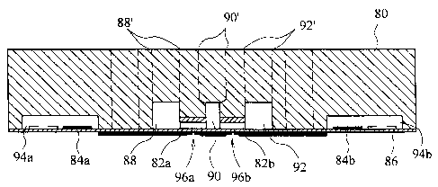
Figures 5 and 6 are exploded perspective and sectional views respectively
of a "pagewide" printhead incorporating both first and second aspects referred
to
above and extending in a direction "W" transverse to a media feed direction P.
In
the sectional view of figure 6, two piezoelectric bodies 82a, 82b each having
channels and electrodes as described above are closed by a substrate 86 in
which
openings 96a,96b for droplet ejection are formed. In accordance with the first
aspect of the invention, respective supply chambers at the ends of the
channels in
each body, namely supply chambers 88 and 90 at either end of body 82a and
supply chambers 90 and 92 at either end of body 82b, are defined between the
substrate 86 and a base 80. Respective channel electrodes are connected to
conductive tracks (not shown) on the substrate 86 as described with regard to
figure 4. These conductive tracks also carry respective driver chips 84a and
84b
located, in accordance with the second aspect of the invention, in further
chambers
94a,94b defined by the base 80. Understandably, the further chambers 94a,94b
are sealed from supply chambers 88 and 92.
This embodiment incorporates a third aspect of the present invention: the
channel-closing substrate 86 with conductive tracks for conveying electrical
signals
to actuator means located in the channels and openings 96a,96b for droplet
ejection acts as a support member for the bodies 82a and 82b. As will be
evident
from figure 5, bodies 82 and drive chips 84 are aligned and fixed to the
substrate
86 - which in turn can be made to such a size as to be easy to handle during
manufacture.
As illustrated in figure 5, bodies 82 may be butted together to form a single,
contiguous, pagewide array of channels - described in W091/17051 and
consequently not in any further detail here - in which case the substrate 86
serves
to support the individual bodies both during and after the butting process.
Such
CA 02290369 2006-04-26
8
bodies may be tested before assembly, thereby reducing the chances of a
complete
printhead being faulty.
The substrate is suitably made of a robust material - such as aluminium
nitride,
INVART"" or special glass AF45 - that has similar thermal expansion
characteristics to the
piezoelectric material of the bodies. It will be appreciated that the
requirement for thermal
matching between bodies and substrate is reduced where there is a gap between
successive butted bodies (the gap advantageously being filled with glue bond
material as
mentioned in the aforementioned W091/17051) in which case a less well
thermally-
matched material such as alumina can be used.
Figure 7 shows detail of a droplet ejection opening 96a formed in the
substrate 86.
Whilst the opening 96a itself may be formed with a taper, it is advantageous
to form the
tapered shape in a nozzle plate 98 mounted over the opening. Such a nozzle
plate may
comprise any of the readily-ablatable materials such as polyimide,
polycarbonate and
polyester that are conventionally used for this purpose.
Furthermore, nozzle manufacture can take place independently of the state of
completeness of the rest of the printhead: the nozzle may be formed by
ablation from the
rear prior to assembly of the active body 82a onto the substrate 86 or from
the front once the
active body is in place. Both techniques are known in the art. The former
method has the
advantage that the nozzle plate can be replaced or the entire assembly
rejected at an early
stage in assembly, minimising the value of rejected components. The latter
method
facilitates the registration of the nozzles with the channels of the body when
assembled on
the substrate.
The construction of figures 5 and 6 has two rows of nozzles formed in a single
nozzle plate extending over both the openings 96a,96b in substrate 86 and
extending the
full length of the substrate. Following the mounting of a corresponding two
rows of bodies
82a,82b and drive chips 84a,84b onto the substrate 86 and suitable testing -
as described,
for example, in EP-A-O 376 606 -
CA 02290369 1999-11-12
WO 98/52763 PCT/GB98/01495
9
base 80 can be attached, thereby to defme manifold chambers 88,90 and 92. In
accordance with a further aspect of the invention, chamber 90 supplies the
ends of
channels formed in both bodies 82a,82b whilst chambers 88 and 92 supply the
other ends
of the channels in bodies 82a, 82b respectively. Conduits through which ink is
supplied
from the outside of the printhead to each chamber are indicated by dashed
lines at 88',90'
and 92'. It will be evident that this results in a particularly compact
construction in which
ink can be circulated from common manifold 90, through the channels in each of
the
bodies (for example to remove trapped dirt or air bubbles) and out through
chambers 88
and 92.
Figure 8 shows partial detail of the mounting of drive chip 84a on the
substrate 86
having output tracks 120,122 which connect drive chip outputs 132,134 to
actuating
electrodes in the body and an input track 110 to drive chip input terminal
130. It will be understood that a drive chip will have many such inputs and
outputs, there being generally
at least twice as many outputs as inputs. 84a indicates the first location on
the substrate
86 at which a drive chip will be placed. However, should the drive chip at
this location
subsequently be found to be faulty - e.g. in the course of testing as
described above - a
replacement chip can be mounted at location 84a' as indicated by dashed lines.
If
necessary, the connections of the faulty chip to the tracks 120 and 122 can be
severed by
cutting through the tracks at points 136 - a laser may be particularly
suitable for this
purpose. The beneficial effect of this measure on manufacturing yield in a
pagewide
printhead - which, as shown in figure 5, may have several tens of driver chips
- will be
evident.
Figure 9 shows another embodiment of this aspect of the invention in which
input
signals are supplied via a bus comprising tracks 110, etc. Connection between
the tracks
110, etc. and chip input terminals 130 is achieved by means of further tracks
150,
deposited on top of tracks 110, etc. and isolated therefrom by a passivation
layer 145.
Should drive chip (integrated circuit die) 84a prove faulty, it is possible to
connect a
replacement chip or die at location 84a', shown dashed in figure 9, which is
spaced from
(falls outside the footprint of) the first chip 84a. A second bus
CA 02290369 1999-11-12
WO 98/52763 PCT/GB98/01495
comprising tracks 110', passivation layer 145' and further tracks 150' is used
to
supply input signals. A further passivation layer 140 underlies the second-
bus,
isolating it from output tracks 120,122,.. which have locations for connection
both to
the output terminals 132,134,.. of chip 84 and and to the output terminals
132',134'
of replacement chip 84'. Excision by means of a laser along line 136 allows a
faulty
chip to be electrically isolated from the output tracks 120,122,.. before a
replacement chip 84' is connected.
The foregoing examples have related particularly to droplet deposition
apparatus utilising piezoelectric material operated in shear mode as the
actuating
mechanism. Such devices are discussed, for example, in the aforementioned
W091/17051, in EP-A-0 364 136 and US-A-5 227 813. The principles outlined
above are equally applicable to other actuating mechanisms however, including
both piezoelectric and thermal (bubble-jet), and in particular to the
arrangements
disclosed in co-pending UK patent application no. 9721555.2.
, ..,.