Note: Descriptions are shown in the official language in which they were submitted.
CA 02290429 1999-11-17
WO 98/56144 PCT/EP98/03063
BROADBAND TELECOMMUNICATIONS SWITCH
The present invention relates to broadband tele-
communications switches which operate to switch packets or cells
of data from a plurality of input ports to a plurality of output
ports. In particular, but not exclusively, the present invention
relates to broadband telecommunications switches which operate
in accordance with Asynchronous Transfer Mode (ATM) principles.
Telecommunications systems which communicate data at
rates in the order of mega bits per second are known as
broadband telecommunications systems. In order to effect
communication of data at such high rates between a plurality of
sources and a plurality of receivers, telecommunications systems
are adapted to make optimum use of an amount of data
communications bandwidth provided by a telecommunications
network. To this end, broadband telecommunications systems
operate to communicate data in a form of discrete packets or cells
which carry a predetermined amount of information. An example
of such a broadband telecommunications system is an
Asynchronous Transfer Mode (ATM) telecommunications system,
wherein data is conveyed in ATM cells. Each ATM cell comprises a
predetermined quantity of data as well as a cell header, which
contains a virtual channel identifier and a virtual path identifier
which are used by nodes or switches of a telecommunications .
network to route the ATM cells between sources and receivers.
To achieve an efficient utilisation of a data communications
bandwidth provided by a telecommunications network, tele-
CA 02290429 1999-11-17
WO 98/56144 PCT/EP98/03063
-2-
communications systems may further operate to provide a
predetermined series of data transport media characterised by
predefined data transmission parameters such as delay, integrity
and cell rate. The telecommunications system is therefore
arranged to provide a series of virtual communications paths, each
of which is arranged to communicate data in accordance with the
predetermined transmission parameters. Such communications
paths are known as bearers, each of which is defined by the
attributes of the data which it is to communicate. Hence, by
selecting an appropriate bearer, a user of the telecommunications
network is provided with a cost effective means for
communicating broadband data in accordance with the type and
attributes of data the user is generating.
Bearer types may include Constant Bit Rate ( CBR) which may
be delay and integrity critical. An example of a service carried by
a CBR bearer is voice or speech data. Other bearer types include
Variable Bit Rate ( VBR) which is provided for data sensitive to
losses and some tolerance to delay, and Available Bit Rate (ABR)
which is loss sensitive but comparatively delay insensitive. There
is also a data bearer type for data which is insensitive to both
delay and integrity, which is known as Unspecified Bit Rate (UBR}.
CBR, ABR, VBR and UBR are defined for ATM in accordance with
the ATM Forum.
In order to switch data received on an input port of a
broadband telecommunications switch to a plurality of output
ports, the broadband telecommunications switch must operate at a
substantially higher rate than the rate at which data is received
r ~ t
CA 02290429 1999-11-17
WO 98/56144 PCT/EP98/03063
-3-
on the input port. To effect the switching operation, a core of the
broadband telecommunications switch operates to interrogate
packets of data received from an input port to determine whichlof
the plurality of output ports the data packets should be sent, and
routes the packets from the input port to the corresponding
output port. If there are n output ports associated with a
broadband telecommunications switch, then the core must operate
at a rate of n multiplied by the bit rate or bandwidth associated
with any input port, if no delay or loss of data is to be incurred in
association with the switching operation. Furthermore, if there
are n input ports, then the rate of processing of the switch core
must be n2 multiplied by the bit rate or bandwidth of receiving
data on any one input port.
In order to reduce the processing rate required of the switch
core, known ATM switches are provided with data buffers which
are operatively associated with each of the input ports, and which
operate to store ATM cells at the input port until an output port to
which they are to be switched has sufficient capacity to receive
these ATM cells. This allows for a substantial reduction in the
processing rate of the switch core. An example of a known ATM
switch is disclosed in granted UK patent number 2272820B.
As with the input ports, a data rate or bandwidth limit for
communicating data is associated with each of the output ports.
Typically, but not exclusively, the data rate of the input ports is
equal to the data rate of the output ports which are also equal to
each other. As such, communications bandwidth associated with
the output port is bandwidth limited, so that a technical problem
CA 02290429 1999-11-17
,- , ~ .~
exists in arranging for data packets received on the input port to be
switched between the output ports whilst accommodating the bandwidth
limit associated with each output port, and insuring that no data packet is
lost in communication between the input ports and the output ports.
In an article entitled "An Output-Buffered ATM Switch in the
Multichannel Bandwidth Allocation Environment ", Electronics and
Communications in Japan, Part I, Vol, 74, No. 6, 1991, a method of
balancing the load allocation among a number of channels in the same
output channel group is disclosed. In this article, an input port controller
sends transmission request packets to a batcher network where they are
sorted and fed back to the controller for channel assignment in
accordance with output bandwidth limitations.
In an article published in IEEE Transactions on Communications,
No. 9, September 1990, New York, US entitled "A Multiservice High-
Performance Packet Switch for Broad-Band Networks ", there is
described an input queued packet switch for broadband networks which
supports data link connections whose capacity is not constrained by the
capacity of a single packet channel. The switch bandwidth is allocated at
two different times. At connections set-up time, an output data link is
selected on which some bandwidth is reserved for the new call. At
transmission time, specific channels within the data link are optimally
allocated, slot by slot, to the packets addressed to that link, solving the
output channel contention at the same time.
The technical problem of switching data packets from a plurality
of input ports to a plurality of output ports, which output ports are
bandwidth limited, is addressed by the present invention.
AME~:~~ SHEET
IPEAIE°
CA 02290429 1999-11-17
. . .", " , , . .
., . . - ~ ~ ' _
-Via- : ~ ~ '
.,
According to the present invention there is provided a broadband
telecommunications switch for switching packets of data received on a
plurality of input transmission lines to a plurality of bandwidth limited
output transmission lines, the switch comprising:- a plurality of input
ports each connected to one of the input transmission lines; a plurality of
output ports each connected to one of the output transmission lines; a
switch core connecting the plurality of input ports to the plurality of
output ports; control processor means for communicating request data for
each of a plurality of switching periods, the request data being
representative of a request for communications bandwidth from the
output ports which is sufficient to accommodate packets of data received
at the input ports during a corresponding switching period; and
bandwidth allocator means for receiving the request data and for
communicating bandwidth allocation data to each of the input ports, the
bandwidth allocator means responding to the communicated request data
by generating bandwidth allocation data appertaining to an allocation of
a share of the bandwidth of the output ports to the input ports, the share
of bandwidth allocated to each input port being used to switch data
therefrom to the output ports; characterised in that the control processor
means comprises a plurality of control processors each operatively
associated with respective ones of the input ports, and the bandwidth
allocator means comprises a plurality of bandwidth allocators each
operatively associated with respective ones of the output ports; and in
that the switch further comprises a data store for storing limit table data
appertaining to a predefined relationship between an amount of data to
be switched from an input port to an output port according to the
bandwidth of the output port.
AMEIV~=-.~; SHEET
IPEA/EP
CA 02290429 1999-11-17
WO 98/56144 PCT/EP98/03063
-S-
The request data may represent a number of data packets
received at the input port during the corresponding switching
period.
Each of said input ports may further include for each output
port a data store for buffering data packets received at the input
port before being communicated to a respective output port via
said switch core. The control processor associated with each input
port may operate to generate request data in accordance with a
number of data packets present in said data stores for
communication to said output ports.
Switching of data packets between input ports and the
output ports of a broadband telecommunications switch
represents a task of some considerable complexity. This is
because there is not only a wide variation in data rates of data
arriving at the input ports of the switch, but also a plurality of
bearer types with different integrity and delay sensitivities. By
arranging for a control processor associated with each input port
to periodically transmit to each of the output ports request data
representative of a bandwidth requirement from the
corresponding output port sufficient to egress the data received at
the input port for a given switching period, the allocation of the
bandwidth of the output ports to the input ports may be effected
in a quasi synchronous manner, the effect of which is to
substantially reduce the complexity of the switch compared to a
switch where bandwidth allocation is executed asynchronously.
CA 02290429 1999-11-17
WO 98/56144 PCT/EP98/03063
-6-
Although allocation of the bandwidth of the output ports is
effected in a quasi synchronous manner, switching of data packets
is effected asynchronously.
The switching period is a period of time for which the
bandwidth allocation of the output ports to each of the input ports
is substantially constant. Determination of the bandwidth
allocation of the output ports to the input ports for the associated
switching period may be determined in correspondence with a
predetermined temporal position within the corresponding
switching period. The corresponding switching period and the
associated switching period may be the same switching period.
The temporal position within the corresponding switching
period at which the bandwidth of the output ports is allocated to
the input ports, may be determined by a polling event.
The polling event may be determined by an common clock
which generates synchronisation signals fed to each of said
control processors.
Each input port may be co-located with an associated output
port so that the control processor of an input port may be
operatively associated with a bandwidth allocator of a
corresponding output port. The polling events may be determined
by a temporal position at which each of the plurality of bandwidth
allocators receives a request data communication from one of said
control processors, in response to which each of the control .
processors operatively associated with the bandwidth allocators
also communicate a request data.
1
CA 02290429 1999-11-17
WO 98/56144 PCT/EP98/03063
_7_
Each of the bandwidth allocators may further include a data
store for storing limit table data appertaining to a predefined
relationship between an amount of data to be switched from an
input port to an output port for a switching period in
correspondence with a bandwidth of the output port to be
allocated to the input port for switching said data. Each of the
control processors associated with the output ports may
furthermore operate in combination with the limit table data to
generate a limited bandwidth allocation determined in
dependence upon a number of data packets to be communicated
from the input port to the output port.
Advantageously, the telecommunications switch may further
operate to switch data from a Constant Bit Rate bearer across the
switch core in preference to other data and to the request data.
The bandwidth of the output ports allocated to the input
ports for switching Variable Bit Rate and Available Bit Rate (ABR)
data, may be that which remains when bandwidth allocated to CBR
bearers is subtracted from a total link bandwidth associated with
the output ports.
The telecommunications switch may further operate to
allocate surplus bandwidth to Unspecified Bit Rate bearers
appertaining to the bandwidth of the output ports which has not
been allocated to the input ports, as a result of a bandwidth
allocation limit determined in dependence upon the limit table.
Advantageously, the control processors may operate to
weight each share of the allocated bandwidth from the output
ports, so that a total of each share of the bandwidth of the output
CA 02290429 1999-11-17
.. . .-
- F
..
ports does not exceed a total link bandwidth of a link communicating the
input port to the switch core.
According to an aspect of the present invention, there is provided
a method of switching data packets from a plurality of input transmission
lines to a plurality of output transmission lines across a broadband
telecommunications switch as described above, the method comprising
the steps of -
(i) generating request data for each input port representative
of a number of data packets to be switched by the input port to respective
output ports;
(ii) contemporaneously switching the request data for each
input port generated in step (i) across the switch core to the respective
output ports;
(iii) determining a share of the bandwidth of the output ports
for each input port in accordance with request data received from the
input ports; and
(iv) conveying bandwidth allocation data corresponding to the
bandwidth of the output ports allocated to each input port across the
switch core to each of the input ports to allocate the bandwidth of the
output ports to the input ports for a predetermined switching period to
effect egress communication of the data packets.
One embodiment of the present invention will now be described
by way of example only with reference to the accompanying drawing,
wherein,
FIGURE 1 shows a schematic conceptual diagram of a broadband
tele-communications switch;
AME ' =i~ SHEET
IP~AIEP
CA 02290429 1999-11-17
" ., ..
_~a_ _ ~~
FIGURE 2 shows a schematic timing diagram of events which
occur during a switching period.
AMEf~.'~~~~ SHEET
I PEA/EP
CA 02290429 1999-11-17
WO 98/56144 PCT/EP98103063
-9-
The example embodiment provided is a broadband
telecommunications switch operating in accordance with
Asynchronous Transfer Mode (ATM) principles. To this end,
Figure 1 shows a schematic block diagram of an ATM
telecommunications switch, designated generally as 1.
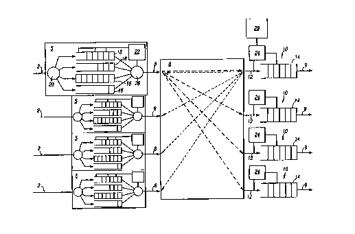
In Figure 1, four input transmission means represented as
lines 2, are shown to feed each of four input ports designated
generally 5. Each of the input ports S, are coupled to an ATM
switch core 6, by conductors 8. Data traversing the switch core 6
is fed to one of the four output ports designated generally 10,
which is thereafter egressed on an output transmission line 9,
which communicates with the rest of a broadband
telecommunications system.
In this example embodiment of the invention, each of the
transmission lines 2, on the input side of the switch, and the
output side of the switch 9, communicate ATM cells at a rate of
150 mega bits per second. As such it is the function of the switch
1, to switch ATM cells from the input conductors 2 to the output
conductors 9, in accordance with the connection identifying
information provided in the header of the ATM cells, which
header contains the virtual path and virtual channel identifiers.
Within the ATM switch 1, the switch core 6 operates to switch the
ATM cells between the input conductors 8 and the output
conductors 12, in accordance with the switching operation. As
hereinbefore explained, the switch core 6, acts as a routing or
switching processor. The switch core G, is provided with some
data storage capacity (not shown) for storing data packets to be
CA 02290429 1999-11-17
r
.. ..
-10-
switched to output ports, in a situation in which input ports send data
packets to the same output port contemporaneously. The data storage
capacity of the switch core 6, therefore operates to de-couple the
switching of data packets between input ports and output ports.
Each of the output transmission lines 9, has a data capacity of 150
mega bits per second and are therefore bandwidth limited. Each output
port further includes a data store 14, which acts as a buffer for ATM cells
which are egressed from the output port 10. The data stores 14, serve to
re-shape ATM cell traffic which is egressed from the output port 10.
As has been previously explained, in order to arrange for the ATM
cells received on each of the input lines 2, to be switched to the output
ports 10 without loss of ATM cells or delay, the switch core 6, would
have to be arranged to switch ATM cells at a rate proportional to the
square of the number of input lines 2, multiplied by the communication
data rate bandwidth on any one of the input ports. This is because in
order to switch data from all of the input ports to one of the output ports,
the ATM switch port 6, would have to operate at a rate proportional to n
multiplied by the data rate of the input line, where n is the number of
input ports, and this data rate would have to be provided for each of the
output ports, hence, the rate of switching of the ATM switch core 6,
would be proportional to n2 multiplied by the data rate on any one of the
input lines. However, in each of the input ports 5, there is provided a
data store 18, for each of the output ports 10. Furthermore, there is also
provided a switching node 20, which
AME '~~ SHEET
IPEAIEP
CA 02290429 1999-11-17
WO 98/56144 PCT/EP98103063
-11-
serves to switch ATM cells received on the input line 2, to each of
the buffers 18, in accordance with the output port to which the
ATM cells are to be switched. This arrangement of the switching
node 20 and the data stores 18, for each of the output ports, has
an effect such that switching of data from the input port to each of
the output ports need only be performed at a rate which is on
average proportional to the data rate of the input line 2.
Therefore, in this case, the rate of operation of the switch core
may be reduced to n multiplied by the communications data rate
bandwidth of any of the input lines 2, and since n = 4, the rate in
this case is 600 mega bits per second.
The ATM switch 1, thus far described, is provided with a
means to separate ATM cells destined for each of the output ports,
into a corresponding number of data stores 18, at each of the
input ports 5. The arrangement by which the ATM switch 1,
switches the ATM cells present in the input buffers of the input
port 5, to the output ports 10, whilst accommodating the
bandwidth limitation of the output ports 10 will now be described.
Each of the input ports 5, is provided with a control
processor 22, which operates to interrogate each of the input data
stores 18, to assess the number of cells present in the data stores
at the start of a switching period. The switching period may, for
example, be in the order of 7ms. The control processor 22,
determines the number of cells stored in data stores 18, which are
to be switched for the current switching period. After
determining the number of cells present in each of the input data
stores 18, the control processor 22 generates an ATM cell which
CA 02290429 1999-11-17
.~ ,
-!2-
contains request data representative of the number of ATM cells in the
data stores 18, at a predetermined temporal position within the
corresponding switching period. This ATM cell containing request data,
hereafter referred to as the request data cell, is fed via conductor 8, to the
ATM switch core 6, which thereafter performs a multicast operation,
wherein the request data cell is replicated and switched to each of the
output ports 10. This operation is repeated by each of the control
processors 22 in each of the input ports S.
At each of the output ports 10, a bandwidth allocator 24, receives
the request data cells via conductor 12, from each of the input ports 5.
As hereinbefore mentioned, the bandwidth of the output port is limited to
the link bandwidth of the conductor 12, which is 150 mega bits per
second. However, a portion of this bandwidth may be allocated to a
Constant Bit Rate (CBR) bearer and so the bandwidth of the link 12,
remaining, after subtraction of the portion allocated to CBR bearers is
that which is available to be shared amongst the input ports in
accordance with the request data cell. The bandwidth allocator 24,
operates to apportion the share of this available bandwidth between the
respective input ports S, in accordance with the request data cells
received therefrom. The bandwidth allocator 24, then transmits a
bandwidth allocation ATM cell containing data representative of the
bandwidth allocated to each of the input ports 5, by the output ports 10,
and the bandwidth allocation cell is multicast across the ATM switch
core 6, so that the same cell is communicated to each of the input ports 5.
This operation is performed by each
AMEI '~.E~ S~IEET
1PEA/EP
CA 02290429 1999-11-17
WO 98/56144 PCT/EP98/03063
-13-
bandwidth allocator 24, for each of the output ports 10. The
bandwidth allocation cells are received by each of the input ports
5, and fed to the control processor 22.
After receiving the bandwidth allocation cells, the control
processors 22, are in receipt of the necessary information to
switch the ATM cells in the input data buffers 18, across the ATM
switch for an associated switching period which may be a next
subsequent switching period. However, the control processor 22,
must perform one further operation before configuring the input
port to switch ATM cells at a desired rate appertaining to the
bandwidth allocation. The further operation is required to ensure
that a total of the shares of allocated bandwidth from each output
port does not exceed a total link bandwidth of the communication
links 8, between the input ports S and the switch core 6. To do
this the control processors 2 2, sum each share of the bandwidth
allocations from the output ports, and when the sum exceeds the
total link bandwidth, scales the bandwidth share so that the total
link bandwidth is not exceeded. For example, if three output ports
operate to provide an input port with a share of 75 mega bits per
second, then the total bandwidth allocated to the input port would
be 225 mega bits per second. Therefore, in this example, the
control processor 22, would be configured in combination with
switching node 26, so that the rate of transmitting ATM cells
across the switch core 6, to each of these output ports is reduced
to 50 mega bits per second. This, of course, will result in some
surplus bandwidth being unused at the output ports. However, it
would present a further level of complexity to re-allocate this
CA 02290429 1999-11-17
WO 98/56144 PCT/EP98/03063
-14-
bandwidth, and since this will only remain unused for one
switching period, this wasted capacity is minimised.
In accordance with the bandwidth allocation, the control
processor 22, operates to feed ATM cells from each of the input
data stores 18, via a switching node 26, to the ATM switching core
6, which thereafter switches the ATM cells to the respective
output ports.
The process of allocating bandwidth of the output ports to
the input ports hereinbefore described is performed for each of a
plurality of switching periods. During a current switching period a
polling event at a predetermined temporal position synchronises
the transmission of the request data by each of the control
processors 22, to the bandwidth allocators 24. This is indicated
conceptually by a timing diagram shown in Figure 2. In Figure 2,
line 30 represents time which increases from left to right. The
time line 30, is divided into a plurality of switching periods of
which switching period 31 is one example. Switching period 31, is
also shown in Figure 2 in an expanded form, in which four events
designated A, B, C and D are indicated conceptionally. Event A is
representative of the transmission of request data by each of the
input ports to each of the output ports. Event B is representative
of the sharing by the bandwidth allocators 24, of the available
bandwidth of the output port amongst the input ports, and the
transmission of the allocation data to the control processors 22,
within the input ports S. Event C is representative of the new
allocation of bandwidth to input ports becoming established,
r.
CA 02290429 1999-11-17
WO 98/56144 PCT/EP98/03063
-15-
whereas event D is representative of the new allocation being
effective for the subsequent switching period.
The arrangement for switching ATM cells between a
plurality of input ports and a plurality of output ports, as herein-
before described with reference to Figure 1, is suitable for ATM
cells which are tolerant to delay. As such, if ATM cells are being
communicated in association with a Constant Bit Rate (CBR) bearer,
which are therefore delay sensitive, the ATM switch operates to
switch these ATM cells, through the switch core 6, to the
corresponding output ports 10, without buffering in any of the
input ports 5 or the output ports 10. It is for this reason that
bandwidth allocated to CBR bearers is subtracted from the total
link bandwidth of the output port to establish the bandwidth
available for sharing with the input ports. The arrangement of
buffering data at the input ports and output ports as hereinbefore
described, is therefore only appropriate for ATM cells conveyed in
association with a Variable Bit Rate (VBR) or Available Bit Rate
(ABR) bearers, wherein the bearer provides for a degree of delay
insensitivity. Furthermore, ATM cells conveyed in association
with an Unspecified Bit Rate (UBR) bearer, will be both delay and
loss insensitive. Therefore, ATM cells conveyed in association
with VBR and ABR bearers will be given priority over ATM cells
conveyed in association with a UBR bearer. As such, the
arrangement for allocating bandwidth of the output ports 10, to
the input ports 5, may be extended to allocating bandwidth to UBR
ATM cells, where surplus bandwidth is available at an output port
10. Surplus bandwidth may be made available by an output port
CA 02290429 1999-11-17
,. . , .. ,
..
.,
in a situation in which there is a demand for a share of the bandwidth
of an output port from one or more of the input ports, for only a
comparatively small number of ABR or VBR ATM cells for a switching
period. If the entire bandwidth of the output port 10, were to be allocated
to these input ports 5, then the ATM cells in the input data stores 18, of
each input port would be switched to the output port in a comparatively
small portion of the switching period. Therefore, in this situation, the
capacity of the output port would remain unused for a substantial portion
of a switching period, whereas it could in fact be used for switching UBR
ATM cells.
To utilise the available surplus bandwidth at any of the output
ports 10, each of the bandwidth allocators 24, is further provided with a
data store 28, which is shown by example for one of the bandwidth
allocators only. Each data store 28, is provided with data representative
of a limit table. The limit table is a predetermined relationship between
an amount of bandwidth of the output ports to be allocated to the input
ports S, and the amount of data present in the input data buffers 18, to be
switched to the output ports 10, such that in the event that a substantial
portion of the bandwidth of an output port is to be allocated to an input
port for which only a relatively small amount of data is to be switched
during a switching period, the limit table determines a limited bandwidth
to be allocated to the input port 5, in proportion to the amount of data to
be switched. So, for example, where the bandwidth of 150 mega bits per
second associated with an output port is to be shared equally between
AMEI'~ :=T' SHEET
lPEA/EP
CA 02290429 1999-11-17
WO 98/56144 PCT/EP98/03063
-17-
two input ports, then without the operation of the limit table, each
port would have a share of 75 mega bits per second. However,
where a relatively small number of cells are present at the input
buffer associated with the input port, the limit table operates to
reduce the 7S mega bits per second to, for example, 10 mega bits
per second, thus freeing a further 65 mega bits per second for
allocation to UBR data services.
An arrangement of input data buffers 18, associated with
the input ports S, is also provided for switching UBR ATM cells in
a substantially similar manner to that described for VBR and ABR
ATM cells, although input data buffers I8, for switching UBR ATM
cells are not shown in Figure 1.
As an alternative arrangement, the output ports may be
provided with a common data store, wherein the limit table data
is stored and accessed by each bandwidth allocator 24.
As will be appreciated by those skilled in the art, various
modifications may be made to the embodiments hereinbefore
described without departing from the scope of the present
invention. In particular, the broadband ATM switch may be any
broadband telecommunications switch which requires packetised
data to be switched between a plurality of input ports to a
plurality of output ports, wherein the bandwidth at the output
port is substantially limited.