Note: Descriptions are shown in the official language in which they were submitted.
CA 02290595 2002-09-09
74611-53 (S)
1
LITHOGRAPHIC IMAGING Y~lITH CONSTRUCTIONS HAVING MIXED
ORGANIC/INORGANIC LAYERS
BACKGROUND OF THE INVENTION
Field of the Invention
The present invention relates to digital printing
apparatus and methods, and more particularly to imaging of
lithographic printing-plate constructions on- or off-press
using digitally controlled laser output.
Description of the Related Art
In offset lithography, a printable image is
present on a printing member as a pattern of ink-accepting
(oleophilic) and ink--rejecting (oleophobic) surface areas.
Once applied to these areas, ink can be efficiently
transferred to a recording medium in the imagewise pattern
with substantial fidelity. Dry printing systems utilize
printing members whose ink-rejecting portions are
sufficiently phobic to ink as to permit. its direct
application. Ink applied uniformly to the printing member
is transferred to the recording medium only in the imagewise
pattern. Typically, the printing member first makes contact
with a compliant intermediate surface called a blanket
cylinder which, in turn, applies the image to the paper or
other recording medium. In typical sheet-fed press systems,
the recording medium is pinned to an impression cylinder,
which brings it into contact with the blanket cylinder.
In a wet lithographic system, the non-image areas
are hydrophilic, and the necessary ink-repelle:ncy is
provided by an initial application of a dampening (or
"fountain") solution to the plate prioz° to inking. The ink-
74611-53(S)
CA 02290595 2002-09-09
2
abhesive fountain solution prevents ink from adhering to the
non-image areas, but does not affect the oleophilic
character of the image areas.
To circumvent the cumbersome photographic
development, plate-mounting and plate-registration
operations that typify traditional printing technologies,
practitioners have developed electronic alternatives that
store the imagewise pattern in digital form and impress the
pattern directly onto the plate. Plate-imaging devices
amenable to computer control include various forms of
lasers. For example, U.S. Patent Nos. 5,351,617 and
5,385,092 describe an ablative recording system that uses
low-power laser discharges to remove, in an imagewise
pattern, one or more layers of a lithographic printing
blank, thereby creating a ready-to-ink printing member
without the need for photographic development. In
accordance with those systems, laser output is guided from
the diode to the printing surface and focused onto that
surface (or, desirably, or3to the layer most susceptible to
laser ablation, which will generally li.e beneath the surface
layer) .
U.S. Patents 5,783,364 and 5,807,658 describe a
variety of lithographic plate configurations for use with
such imaging apparatus. In general, the plate constructions
include an inorganic layer (i.e., a metal, combination of
metals, or a metal/non-metal compound? situated on an
organic polymeric layer. The inorganic layer ablates in
response to imaging (e.g., infrared, ar "IR") radiation. In
one approach, the inorganic layer represents tike topmost
surface of the plate and acce~ats fountain solution, while
the underlying polymeric layer accepts ink, In another
CA 02290595 2002-09-09
?4611-53 (S)
2a
approach, the inorganic layer serves only a radiation-
absorption (rather than a lithographic) function, with the
underlying layer accepting i.nk and an overlying layer either
rejecting ink or accepting fountain solut:i.on. Ablation of
the inorganic layer by an imaging pulse generally weakens
the topmost layer as well, and this, combined with
disruption of its anchorage (due to disappearance of the
ablated inorganic layer), renders the
CA 02290595 2003-08-05
74611-53(S)
3
topmost layer easily removable in a post-imaging cleaning
step. With either of these two approaches, application of
an imaging pulse to a point on the plate ultimately creates
an image spot having an affinity for ink or an ink-abhesive
fluid differing from that of unexposed areas, the pattern of
such spots f=orming a lithographic plate image.
These types of plates can pose manufacturing
challenges, as well as performance limitations, owing to the
abrupt transition between an inorganic layer and an organic,
polymeric layer. The divergent physical and chemical
characteristics of such distinct layers can compromise their
anchorage to one another - a critical performance
requirement - as well as the durability of the inorganic
layer. For example, because inorganic and organic materials
typically have very different coefficients of thermal
expansion and elastic moduli, even perfectly adhered
inorganic layers may undergo failure (e.g., fracturing) due
to temperature variations or the stress of plate
manipulation and use. The different responses of two
adjacent layers to an external condition can easily cause
damage that would not occur in either layer by itself.
To improve interlayer anchorage, polymeric layers
may be selected (or applied as intermediate coatings) based
on chemical compatibility with inorganic material. A
polymeric layer may also be pretreated (e. g., through plasma
exposure) to modify the surface fo:r greater interfacial
compatibility with a subsequently <applied inorganic layer.
These approaches, however, have limited utility in
addressing i~he effects of transition between fundamentally
different materials.
CA 02290595 2003-08-05
74611-53(S)
3a
DESCRIPTION OF THE INVENTION
Brief Summax=y of the Invention
In one aspect of the present invention, there is
provided a method of printing comprising: a. providing a
printing member fabricated according to steps comprising:
i. providing a first layer comprising a curable polymer and
having a first surface; ii. softening the first layer;
iii. depositing onto the first sur.~ace of the softened first
layer a deposition material comprising an inorganic
compound, the deposition material depositing onto the
surface and integrating within the first layer; iv. curing
the first layer to immobilize the integrated deposition
material; and v. applying a second layer over the deposition
material and any exposed portions of the first surface,
wherein (a) at least the second layer has a different
affinity from the first. layer for at least one printing
liquid selected from the group consisting of ink and an
abhesive fluid for ink, and (b) at least the second layer,
but not the first layer, is subject to ablative removal by
exposure to laser radiation; b. se:Lectively exposing, in a
pattern representing an image, the printing member to laser
output so as to ablate selected portions of at least the
second layer, thereby directly producing an array of image
features; c. applying i.nk to the member; and d. transferring
the ink to a recording medium.
In a second aspect, there is provided a method of
fabricating a lithographic printing plate, the method
comprising: a. providing a first layer comprising a curable
polymer and having a first surface; b. softening the first
layer; c. depositing onto the first surface of the softened
first layer a deposition material comprising an inorganic
CA 02290595 2003-08-05
74611-53(S)
3b
compound, the deposition material depositing onto the first,
surface and integrating within the first layer; d. curing
the first layer to immobilize the integrated deposition
material; e. applying a second layer over the deposition
material and any exposed portions of the first surface,
wherein f. at least the second layer, but not the first
layer, is subject to ablative removal by exposure to laser
radiation; and g. the second layer and at least the first
layer have different affinities for at least one printing
liquid selected from the group con:>isting of ink and an
abhesive fluid for ink.
The present invention reduces the abruptness of
interfacial transition by altering the effective properties
of the organic layer (to which the inorganic layer is
applied) by incorporating an inorganic component within the
matrix of the organic layer. One E:embodiment of the
invention comprises a method of fabricating a lithographic
printing plate having
74611-53 (S)
CA 02290595 2002-09-09
4
adjacent organic and inorganic layers. A first layer
comprising a curable polymer is softened, and an inorganic
material -- compatible with ar, in some cases,
compositionally identical. to -- the soon-to-be-applied
inorganic layer is deposited onto a surface o;E the softened
polymer. The inorganic material overspreads t:he surface and
integrates within the soft polymeric Layer; at. this point,
it may be desirable to assist the migration oi= the inorganic
material into the polymer (e. g., by charging t:he inorganic
material and applying an opposite charge t.o a conductor
underlying the polymer). The polymer is then cured to
immobilize the integrated deposition matex-ial, thereby
forming a composite, and the desired :inorganic: layer is
applied over the deposited inorganic material (and any
exposed portions of the polymer). This second inorganic
layer, and possibly the previously deposited inorganic
material as well, is subject to ablati~re removal by exposure
t.o laser radiation. The second inorganic layer and the
organic/inorganic composite have different affinities for
ink and/or an ink-abhesive fluid. The inorganic layer may,
for example, be a metallic inorganic material as disclosed
in previously referenced U.S. patents 5,783,364 and
5,807,658. Despite the introduction of such an inorganic
material within the matrix of the polymer, the natural
affinity characteristics (e.g., oleophi.licity) of the
polymer may be retained. For example, while the inorganic
phase may have a pronounced effect on the stiffness and
heat-transport properties of ~he composite, thereby
enhancing physical compatibility with a. pure inorganic
layer, it may not significant:Ly affect surface energy (so
that the composite retains the affinity for ink and/or an
ink-abhesive fluid that characterized t:he original polymer).
CA 02290595 2002-09-09
74611-53(S)
The deposition material may fully cover the
surface of the polymeric material, forming a continuous
layer thereover, or may instead form an intermittent pattern
over the surface. In the former case, imaging radiation may
5 remove both the second inorganic layer and the deposition
material from the polymer to expose the surface of the
<:omposite .
The polymer is generally chosen both for its
lithographic affinity characteristics and also for its
ability to be cured into a rigid, three-di.men~~ional
structure that permanently immobilizes the inorganic
deposition material. Not suitable for the present invention
are polymeric materials that exhibit a :Low glass-transition
temperature (which permits repeated, temperature-dependent
transitions between soft and rigid states) unless provided
with crosslinking groups that facilitate permanent cure(and
thereby defeat further phase transitions). In. a preferred
embodiment, the polymer comprises an acrylic polymer
combined with a multifunctional acrylate monomer, which are
crosslinked following deposition of the inorganic material.
Acrylates, like many inorgani~~ deposit:a..on materials, can be
deposited under vacuum, permitting the entire fabrication
process to be carried out in a single operation.
In general, the deposition material will be ink-
receptive and the second layer hydrophilic. This need not
be the case, however, nor do these affinity characteristics
mandate a wet plate. For example, as described in U.S.
Patent No. 5,783,364, the second layer can underlie a
topcoat having a different affinity characteristic.
Ablation of the second layer disrupts the anchorage of the
topcoat, rendering it easily removed in a post-imaging
CA 02290595 2003-08-05
74611-53(S)
5a
cleaning step to reveal the deposition material (and
possibly the polymeric layer as well). The topcoat may be
silicone or a fluoropolymer in the case of a dry plate, or a
hydrophilic polymer if a polymer-tcpcoated wet plate is
desired. Of course, application of a polymeric layer over
the inorganic second layer raises the same compatibility
issues resolved through use of the inorganic deposition
material.
In a second embodiment, d graded structure is
built up on a substrate in successive deposition steps.
Both polymer precursors and an inorganic filler material are
deposited in stages, with each stage containing a desired
ratio of polymer to filler. In a preferred embodiment, the
proportion of filler increases in each stage, resulting in a
concentration gradient with the amount of filler increasing
away from the substrate. The polymer precursors may be
cured after each stage of
CA 02290595 1999-11-22
WO 99/48689 PCT/US99/05613
-6-
deposition, permanently immobilizing the distribution of
organic and inorganic material. A top layer is applied over a
surface of the structure, the top layer and the surface having
different affinities for ink and/or an ink-abhesive fluid. The
s top layer, but~not the underlying graded structure, may be
subject to ablative removal by exposure to laser radiation.
The polymer precursor and the filler material may be
deposited as a vapor or as a liquid. In one embodiment, the
precursor is an acrylic polymer combined with a multifunctional
o acrylate monomer, the curing step crosslinking the monomers
with the polymer. Once again, the structure is typically
oleophilic and the deposited inorganic layer hydrophilic, but
the result need not be a wet plate.
In use, a printing plate in accordance with the invention
is selectively exposed, in a pattern representing an image, to
imaging radiation (emanating, for example, from one or more
lasers whose output is scanned over the surface of the plate)
so as to ablate selected portions of the inorganic layer and,
possibly, exposed portions of the deposition material, thereby
zo directly producing an array of image features. Ink is applied
to the plate and transferred to a recording medium in the
conventional fashion. As used herein, the term "plate" or
"member" refers to any type of printing member or surface
capable of recording an image defined by regions exhibiting
zs differential affinities for ink and/or fountain solution;
suitable.configurations include the traditional planar
lithographic plates that are mounted on the plate cylinder of a
printing press, but can also include cylinders (e. g., the roll
surface of a plate cylinder), an endless belt, or other
so arrangement.
Brief Description of the Drawincts
The foregoing discussion will be understood more readily
from the following detailed description of the invention, when
35 taken in conjunction with the accompanying drawings, in which:
FIG. 1 is an enlarged sectional view of a lithographic
plate having a mixed organic/inorganic substrate, an
74611-53 (S)
CA 02290595 2002-09-09
7
inorganic layer thereover, and an optional topmost
polymeric layer; and
FIG. 2 is an enlarged sectional view of a
lithographic plate having a graded
organic/inorganic substrate and an inorganic layer
thereover.
Detailed Description of the Preferred Embodiments
Imaging apparatus suitable for use in conjunction
with the present printing members includes at least one
laser device that emits in the region of maximum plate
responsiveness, i.e., whose lambdamaX closely approximates
the wavelength region where the plate absorbs most strongly.
Specifications for lasers that emit irn the near-IR region
are fully described in the '617 and '092 patents; lasers
emitting in other regions of the electromagnetic spectrum
are well-known to those skilled in the art.
Suitable imaging configurations are also set forth
in detail in the '617 and '092 patents. Briefly, laser
output can be provided directly to the plate surface via
lenses or other beam-guiding components, or transmitted to
the surface of a blank printing plate from a remotely sited
laser using a fiber-optic cable. A controller and
associated positioning hardware maintains the beam output at
a precise orientation with respect to the plate surface,
scans the output over the surface, and activates the laser
at positions adjacent selected points or areas of the plate.
The controller responds to incoming image signals
corresponding to the original document or picture being
copied onto the plate to produce a precise negative or
positive image of that original. The image signals are
74611-53(S)
CA 02290595 2002-09-09
7a
stored as a bitmap data file on a computer. Such files may
be generated by a raster. image processor (RIP) or other
suitable means. For example, a RIP can ac~cept~ input data in
page-description language, which defines all of the features
required to be transferred onto the p:r:inting plate, or as a
combination of page-description language and one or more
image data files.
CA 02290595 1999-11-22
WO 99/48689 PCT/US99/05613
_g_
The bitmaps are constructed to define the hue of the color as
well as screen frequencies and angles.
The imaging apparatus can operate on its own, functioning
solely as a platemaker, or can be incorporated directly into a
s lithographic printing press. In the latter case, printing may
commence immediately after application of the image to a blank
plate, thereby reducing press set-up time considerably. The
imaging apparatus can be configured as a flatbed recorder or as
a drum recorder, with the lithographic plate blank mounted to
the interior or exterior cylindrical surface of the drum.
obviously, the exterior drum design is more appropriate to use
_in situ, on a lithographic press, in which case the print
cylinder itself constitutes the drum component of the recorder
or plotter.
is In the drum configuration, the requisite relative motion
between the laser beam and the plate is achieved by rotating
the drum (and the plate mounted thereon) about its axis and
moving the beam parallel to the rotation axis, thereby scanning
the plate circumferentialiy so the image "grows" in the axial
zo direction. Alternatively, the beam can move parallel to the
drum axis and, after each pass across the plate, increment
angularly so that the image on the plate "grows"
circumferentially. In both cases, after a complete scan by the
beam, an image corresponding (positively or negatively) to the
25 original document or picture will have been applied to the
surface of the plate.
In the flatbed configuration, the beam is drawn across
either axis of the plate, and is indexed along the other axis
after each pass. Of course, the requisite relative motion
so between the beam and the plate may be produced by movement of
the plate rather than (or in addition to) movement of the beam.
Regardless of the manner in which the beam is scanned, it
is generally preferable (for on-press applications) to employ a
plurality of lasers and guide their outputs to a single writing
35 array. The writing array is then indexed, after completion of
each pass across or along the plate, a distance determined by
the number of beams emanating from the array, and by the
CA 02290595 2002-09-09
WO 99/48689 PCT/US99/056t~
-9-
desired resolution (i.e., the number of image points per unit
length). Off-press applications, which can bE: designed to
accommodate very rapid plate movement (e.g., t:hrough use of
high-speed motors) and ~.nereby utilize high laser pulse rates,
s can frequently utilize a single laser as an imaging source.
Representative printing members in accoi:dance with the
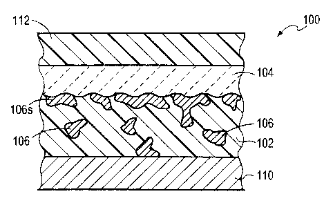
present invention are illustrated in FIGS. 1 and 2. In FIG. 1,
a printing plate 100 comprises a polymeric layer 102 and an
inorganic layer 104. A deposition material 106 is integrated
within the matrix of polymer 102 and, covering all or much of
the entire top surface thereof, provides a transition layer
106s between layers 102 and 104. While material 106 may in
fact be no more chemically compatible with the polymer of layer
102 than would be the inorganic material of layer 104, its
~s physical integration within the matrix of layer 102 affords
strong mechanical adhesion. As shown, the surface layer 106s
extends into the matrix of polymer 102 as a series of
projections or "nails." The firmly anchored layer 106s is
chemically compatible with inorganic layer 104 and therefore
Za exhibits substantial adhesion to this layer.
Plate 100 may be manufactured as follows. A substrate
110, which may be metal, plastic (e.g., polyester), paper, or
some other durable graphic-arts material, accE~pts a coating of
a polymeric material to form layer 102. This polymeric
zs material may, for example, be an acrylic polymer soluble in
methyl ethyl ketone (MEK) and/or other solvents. The acrylic
polymer is combined with selected multifunctional acrylate
monomers and coated (cast) from solvent onto substrate 110.
The multifunctional acrylate acts as a typical ester
3o plasticizer, promoting adhesion and lowering 'the softening
(melting) point of the polymer mixture. The ACRYLOID acrylic
polymers*B-44; *B-'72, and *B-82supplied by Rohm & Haas,
represent suitable solvent-soluble acrylir~s°
dipentaerythritolpentaacrylate (e. g., the *SFZ-399 product
ss supplied by Sartomer) represents a suitable multifunctional
acrylate.
* Trade-mark
CA 02290595 1999-11-22
WO 99/48689 PCT/US99/05613
-10-
The substrate-borne acrylic mixture is heated to the
softening point, whereupon deposition material 106 is applied
to the exposed surface thereof. Material 106 may comprise one
or more metals and/or metal alloys, intermetallics (i.e., two
s or more metals combined in a definite ratio), and/or
compositions including one or more metals in combination with
one or more nonmetals. Preferred nonmetals for such
compositions include boron, carbon, nitrogen, oxygen, fluorine,
and silicon. Material 106 may also be a hard inorganic
compound such as silicon dioxide. It should be stressed that
the deposition material can comprise a plurality of different
substances fulfilling the foregoing criteria.
Material 106 may be applied by conventional roll (web)
coating, or by intermittent-motion machines such as those
~s employed for glass coating. Alternatively, material 106 may be
applied by a vacuum coating process such as vacuum evaporation,
electron-beam (EB) evaporation, or sputtering. The
implementational details of such processes are well-
characterized in the art. The deposition process may involve
zo controlled cooling to withdraw the latent heat resulting from
condensation of the inorganic material from the vapor phase.
With the polymer 102 still in the softened state, it may
be desirable to assist the migration of inorganic material 106
into polymer 102 in order to form the projections discussed
2s above. One approach is to statically charge the inorganic
material 106 and apply an opposite charge to substrate 110.
Layer 102 is then cured, causing it to intensively
crosslink and thereby "freeze" the inorganic material 106 to
impart permanence. An acrylate layer 102 can be cured by EB
3o exposure. The cured polymer exhibits substantially greater
temperature resistance than the original, uncured polymer (that
is, following cure, layer 102 can no longer be readily
softened) and its solubility in the solvents) from which it
was originally coated is substantially decreased, if not
ss eliminated.
Layer 104 is then applied to the surface 106s (which
typically includes exposed portions of layer 102, since it is
CA 02290595 1999-11-22
WO 99/48689 PCT/US99/05613
-11-
generally not necessary to ensure complete coverage of layer
102 by inorganic material 106), typically by vacuum deposition.
Layer 104 may, for example, be a very thin (50-500 ~1, with 300
A preferred for titanium) layer of a metal that may or may not
s develop a native oxide surface upon exposure to air. This
layer ablates in response to IR radiation, and an image is
imposed onto the plate through patterned exposure. The metal
or the oxide surface thereof exhibits hydrophilic properties
that provide the basis for use of this construction as a
lithographic printing plate. Imagewise removal, by ablation,
of layer 104 exposes surface 106s; if fully covered by
inorganic material 106, this layer, too, may be ablated to
expose the surface of composite layer 102. The ultimately
exposed layer is chosen for oleophilicity; accordingly, while
~s layer 104 accepts fountain solution, layer 102 and/or inorganic
material 106 reject fountain solution but accept ink.
The metal of layer 104 in this embodiment is at least one
d-block (transition) metal, aluminum, indium or tin. In the
case of a mixture, the metals are present as an alloy or an
zo intermetallic. Again, the development, on more active metals,
of an oxide layer can create surface morphologies that improve
hydrophilicity.
Alternatively, layer 104 may be a hard, durable,
hydrophilic, metallic inorganic layer comprising a compound of
zs at least one metal with at least one non-metal, or a mixture of
such compounds. Once again, layer 104 ablatively absorbs
imaging radiation, and consequently is applied at a thickness
of only 100-2000 ~. The metal component of layer 104 in this
form may be a d-block (transition) metal, an f-block
so (lanthanide) metal, aluminum, indium or tin, or a mixture of
any of the foregoing (an alloy or, in cases in which a more
definite composition exists, an intermetallic). Preferred
metals include titanium, zirconium, vanadium, niobium,
tantalum, molybdenum and tungsten. The non-metal component may
35 be one or more of the p-block elements boron, carbon, nitrogen,
oxygen and silicon. A metal/non-metal compound in accordance
herewith may or may not have a definite stoichiometry, and may
CA 02290595 2002-09-09
74611-53 (S)
12
in some cases (e. g., A1--Si compounds) be an alloy.
Preferred metal/non-metal combinations include TiN, TiON,
TiOX (where 0.9 s x s 2.0), TiC, and TiGN.
If desired, an additional layer 112 can be applied
over layer 104 to achieve different affinity or physical
characteristics. For example, layer 112 may be a silicone
or fluoropolymer material that rejects ink, thereby
transforming construction 100 into a dry plate. During
imaging, ablation of layer 1.04 disrupts the anchorage of
layer 112, rendering it easily removed :in a post-imaging
cleaning step to reveal the surface 106s or layer 102.
Useful materials .for layer 112 and techniques of coating are
disclosed in U.S. Patent Nos. 5,339,737 and Re. 35,512.
Basically, suitable silicone materials are applied using a
wire-wound rod, then dried and heat-cured to produce a
uniform coating deposited at, for example, 2 g/m2.
A second plate embodiment is shown in FIG. 2. In
this case, the construction 150 includes a graded layer 155
having a concentration of inorganic material 106 that
increases with distance from substrate 110. Layer 155 is
built up in successive stages as follows. A first coating
160 of polymeric material 102 is applied onto substrate 110,
preferably either by vapor condensation or by coating.
Particularly if layer 106 is deposited under vacuum,
polymeric materials amenable to similar deposition
conditions may be preferred for layer 102, allowing
consecutive layers to be built up in multiple depositions
within the same chamber or a linked series of chambers under
common vacuum, One suitable approach is detailed in U.S.
Patent Nos. 5,440,446; 4,954,371; 4,696,719; 4,490,774;
4,647,818; 4,842,893 and 5,032,461. In accordance
74611-53(S)
CA 02290595 2002-09-09
13
therewith, an acrylate monomer is applied as a vapor under
vacuum. For example, the monomer may be flash evaporated
and injected into a vacuum chamber, where it condenses onto
the surface, The monomer is subsequently cro:~slinked by
exposure to actinic (generally ul.travi.olet, or. UV) radiation
or an EB source.
A related approach is described in U.S. Patent No.
5,260,095. In accordance with this patent, an acrylate
monomer may be spread or coated onto a surface under vacuum,
rather than condensed from a vapor. Again, the deposited
monomer is crosslinked by UV or EB exposure.
Either of these approaches may be used to apply
layer 102 onto substrate 110. Moreover, their' applicability
is not limited to monomers; oligomers or larger polymer
fragments or precursors can be applied in accordance with
either technique, and subsequently crossli.nked. Useful
acrylate materials include conventional. monomers and
oligomers (monoacrylates, diacrylates, methacrylates, etc.),
as described at Cols. 8-10 of the 446 patent, as well as
acrylates chemically tailored for particular applications.
Representative monoacrylates include isodecyl acrylate,
lauryl acrylate, tridecyl acrylate, caprolactone acrylate,
ethoxylated nonyl phenyl acrylate, isobornyl acrylate,
tripropylene glycol methyl ether monoacrylate, and neopentyl
glycol propoxylate methylether monoacrylate; useful
diacrylates include 1,6-hexanediol diacrylate, tripropylene
glycol diacrylate, polyethylene glycol (200) diacrylate,
tetraethylene glycol diacrylate, polyethylene glycol (400)
diacrylate, polyethylene glycol (600) diacrylate,
propoxylated neopentyl glycol diacrylate, the '*IRR-214
product supplied by UCB Radcure (aliphatic diacrylate
* Trade-mark
74611-53(S)
CA 02290595 2002-09-09
13a
monomer), propoxylated 1,6-hexanedial diacrylate, and
ethoxylated 1,6-hexanediol di.acrylate; and useful
triacrylates include trimethylolpropane triacrylate (TMPTA)
and ethoxylated TMPTA.
Finally, acrylate-functional or other suitable
resin coatings can be applied onto substrate 7_10 in routine
fashion (under atmospheric canditions?, according to
techniques well-known in the art. In one such approach, one
or more acrylates are coated directly onta substrate 110 and
later cured. In another approach, one or more acrylates is
combined with a solvent (or solvents) and cast onto
substrate 110, following
CA 02290595 1999-11-22
WO 99/4$689 PCT/US99/05613
-14-
which the solvent is evaporated and the deposited acrylate
eventually cured. Volatile solvents, which promote highly
uniform application at low coating weights, are preferred.
Acrylate coatings can also include non-acrylate functional
s compounds soluble or dispersible into an acrylate.
Alternatives to acrylate polymers are of course possible.
For example, it may be desirable to utilize an energetic
organic material (such as an acetylene derivative, an azido or
azide derivative, or a vitro-functional compound) that can
generate gas -- typically explosively -- when the overlying
inorganic layer 104 is heated.
After layer 160 of polymer 102 is applied but prior to
curing, the inorganic filler 106 is applied onto polymer 102 in
a desired ratio relative to polymer 102. In an uncured state,
~s polymer 102 accepts inorganic material 106 in a manner
analogous to a thermally softened layer as described above.
Generally, it is not necessary to draw material 106 into layer
160, since layer 160 is generally quite thin. Particularly
when applied by deposition techniques such as reactive
zo sputtering, material 106 can form a pattern of patches or
islands over the surface layer 160, which is then cured as set
forth above.
Application of layer 160 by vapor condensation affords
greater control over the pattern of deposition. Polymer 102
Zs can be applied under conditions that do not permit coalescence
and consequent film formation, thereby allowing creation of a
discontinuous polymer layer. Inorganic material 106 is then
deposited over the discontinuous pattern, so that the organic
layer is effectively bound within the inorganic material rather
so than vice versa. As discussed above, application of material
106 from vapor generally requires provision for removal of the
latent heat of condensation.
Following deposition and curing of layer 160, the process
is repeated for subsequent layers 162, 164, 166, which are
35 applied with different ratios of inorganic material 106 to
polymer material 102. Preferably, the proportion of inorganic
material increases in each stage, resulting in a graded
CA 02290595 2002-09-09
WO 99/48689 PCT/US99/05613
-15-
structure with the amount of inorganic material increasing away
from substrate 110 as illustrated. The composite layer 155
provides a gradual transition from an organic polymer to a
mixed organic/inorganic material. The dispersed islands of
s inorganic material can be made to occur in "units° (grains,
particles, crystals, etc.) that are one or more orders of
magnitude smaller than solids traditionally d:i.spersed in
organic binders as pigments.
Alternatively, it is possible to apply layers 160-166
without individually curing each layer before applying the next
one, i.e., delaying curing until the entire sequence of layers
has been applied. This approach may provide efficiency and
processing benefits.
Following completion of layer 155, layer 104 is applied
s as discussed above and, once again, an optional layer 112 can
be added thereover.
It will therefore be seen that the foregoing techniques
provide a basis for improved lithographic printing and superior
plate constructions. The terms and expressions employed herein
zo are used as terms of description and not of limitation, and
there is no intention, in the use of such terms and
expressions, of excluding any equivalents of the features shown
and described or portions thereof, but it is :recognized that
various modifications are possible within the scope of the
z5 invention claimed.