Note: Descriptions are shown in the official language in which they were submitted.
CA 02291322 1999-11-30
BACKGROUND OF THE INVENTION
I. field of the Invention
The present invention relates to electrical connectors and, more particularly,
is
directed towards a modular connector or jack which is designed to couple a
modular plug to a printed circuit board.
ll. Description of the Re/atedArt
Modular jacks for coupling modular plugs to printed circuit boards are well
known in the art. See, for example, my prior U. S. Pat. Nos. 4,457,570;
4,501,464;
and 4,717,217. The modular jacks described in my earlier patents are all
characterized by the provision of a dielectric housing and a plurality of side-
by-side
conductors located within the housing. Each of the conductors includes a
spring
contact portion at the front of the housing for mating with a contact terminal
of a
mating modular plug, an end portion at the rear of the housing for connection
to a
printed circuit board, and an intermediate portion disposed between the spring
contact portion and the end portion. The conductors are further characterized
in
2o that the spacing between adjacent spring contact portions is less than the
spacing
between adjacent end portions. For example, the spacing between adjacent
spring
contact portions is preferably 0.040" in order to properly mate with the
contact
2
CA 02291322 1999-11-30
'.
terminals of a modular plug. Further, the spacing at the end portions is
generally
0.050" in order to mate with standard grid spacing for a printed circuit board
(PCB).
The fact that the spring contact portions at the front end of the connector
are spaced
differently from the end portions at the rear end of the connector shall be
referred to
hereinafter as differential spacing.
In addition, the spacing at the rear of the housing where the end portions are
located are formed in two rows which are themselves spaced apart a distance
equal
to twice the adjacent conductor spacing. This pattern of the end portions
forms
to what will be referred to hereinafter as an alternating, staggered array.
Another characteristic of my above-noted prior U.S. patents is that the spring
contact portions of the conductors enter the plug-receiving cavity from the
rear
towards the front thereof. A number of other modular jacks have been designed
whereby the spring contact portions enter the plug-receiving-cavity from the
front
and are angled towards the rear of the cavity. See, for example, U.S. Pat.
Nos.
4,210,376; 4,269,467 and 4,296,991. The conductors in these latter jacks also
exhibit differential spacing, and the end portions, which are coupled to the
PCB, are
also arranged in an alternating, staggered array.
Recently, modular jacks have developed noise problems. These generally
stem from unwanted harmonics or noise from an adjacent line. Such noise could
3
CA 02291322 1999-11-30
also come from radiation in the air or on the cable, or the noise could be
internally
coupled from the outputs of different devices. The tiny chips with which the
modular jacks are utilized to run at very high frequencies, which also
generates
noise in the cabinet.
The danger of noise, of course, is that it could produce a variation in the
amplitude of the signals on the lines. This could, in turn, result in a false
positive,
or could undesirably cancel another signal.
to It has therefore recently become apparent that some type of filtering
mechanism is necessary for use with these modular jacks for eliminating or
greatly
reducing this unwanted noise. It is towards this end that the present
invention is
advanced. .
OBJECTS AND SUMMARY Of THE INVENTION
It is therefore a primary object of the present invention to provide a modular
jack which includes means for reducing the noise on the conductors of the
jack.
Another object of the present invention is to provide a modular jack with
filtering means that is located entirely within the housing of the modular
jack.
4
_.___...._ . __. ...._....-__ ..___..._.___ __.. ____ _ . ... . .
CA 02291322 1999-11-30
~_\
A further object of the present invention is to provide a filtered modular
jack
which can provide a wide range of selected capacitance for filtering the
signals on
the conductors of the jack.
s
An additional object of the present invention is to provide means for
filtering
the signals in a modular jack which may be utilized with any of the wide
variety of
modular jacks currently on the market.
1o A still further object of the present invention is to provide a modular
jack for
coupling a modular plug to a printed circuit board with means fixably coupled
to
the conductors of the jack for filtering the signals appearing on the
conductors.
The foregoing and other objects are achieved in accordance with one aspect
1s of the present invention through the provision of a modular jack for
electrically
connecting a modular plug to a printed circuit board. The jack is of the
having a
dielectric housing within which are positioned a plurality of side-by-side
conductors. Each of the conductors includes a spring contact portion adapted
to
mate with a contact member in the modular plug, an end portion adapted to be
2o connected to the printed circuit board, and an intermediate portion located
between
the spring contact portion and the end portion. The end portions are arranged
in an
alternating, staggered array. The modular jack of the invention comprises
means
CA 02291322 1999-11-30
s ,
located in the housing in electrical contact with the - intermediate portions
of the
conductors for providing a capacitor in series with each of the conductors.
More particularly, the means for providing a capacitor in series with each of
the
conductors comprises a first capacitor module means for providing a first set
of
capacitors in electrical contact with a first set of intermediate portions of
the
conductors, and a second capacitor module means for providing a second set of
capacitors in electrical contact with a second set of intermediate portions of
the
conductors.
In accordance with other aspects of the present invention, the first and
second
capacitor module means comprise first and second substantially planar
substrates,
respectively. The first and second substantially planar substrates are
preferably
positioned in the housing substantially parallel with one another. In one
embodiment, the first and second substrates are located on opposite sides of
the
intermediate portions of the conductors, while in an alternate embodiment, the
first
and second substrates are located on the same side as the intermediate
portions of
the conductors.
2o Alternately, the first and second substrates may be positioned in the
housing
substantially co-planar with one another.
6
T _.~_~..~ _. . ~...~...~... _ _..._ __.~_ ___ . .
CA 02291322 2004-O1-21
In accordance with more specific aspects of the present invention, each of the
first and second substrates preferably comprises a front side, and a back side
which is
parallel with and spaced from the front side. The front side preferably
includes a
plurality of conductive traces formed thereon, while the back side has a
ground plane
formed thereon. More specifically, each conductive trace comprises a
capacitor, and
is substantially U-shaped. The U-shaped capacitors have two legs, one of which
is
electrically connected to an intermediate portion of one of the conductors of
the modular
jack. The front sides of the first and second substrates are preferably closer
to each
other than their respective back sides. There further may be provided ferrite
rod means
connected to the conductive traces for providing further filtering.
In accordance with another aspect of the present invention, the first
substrate
further includes a plurality of fingers projecting from one edge thereof. One
of the legs
of each of the U-shaped capacitors on the front side of the first substrate
preferably
extends along the fingers thereof and includes a roll-over portion extending
over the
edge of the respective finger. In addition, one of the two legs on the front
side of the
second substrate preferably includes a roll-over portion extending over the
edge of the
second substrate. In this embodiment, a third substrate is preferably located
between
the first and second substrates for insulating each from the other in
accordance with
another aspect of the present invention, the first and second capacitor module
means
may comprise first and second
7
CA 02291322 1999-11-30
I_1
complimentary substrates, respectively. The first and second complimentary
substrates are preferably positioned on opposite sides of the intermediate
portions of
the conductors. Each of the first and second substrates comprises a front
side, and a
back side which is parallel with and spaced from the front side, the front
side
having a plurality of conductive formed thereon, the back side having a ground
plane formed thereon.
In accordance with another aspect of this embodiment, the first and second
complimentary substrates each include a plurality of fingers extending from
one
1o edge thereof, the fingers from the first and second complimentary
substrates
adapted to interfit with each other. The intermediate portions of the
conductors are
positioned adjacent the tips of the fingers of the first and second
complimentary
substrates.
is In accordance with more specific aspects of the present invention, the
front side
of the first substrate includes a first set of conductive traces which extend
along the
fingers of the first substrate and which include first roll-over portions that
extend
over the front face of the fingers. In addition, the front side of the second
complimentary substrate includes a second set of conductive traces which
extend
2o along the fingers of the second substrate and which include second roll-
over
portions that extend over the front face of the fingers. In addition, the
front side of
the first complimentary substrate further preferably includes a third set of
8
CA 02291322 1999-11-30
conductive traces which extend parallel to and between the first set of
conductive
traces, the third set of traces preferably including third roll-over portions
that extend
over the edge of the spaces between the fingers of the first substrate.
In accordance with more specific aspects of the latter embodiment, the first
set
of conductive comprises the first set of capacitors, while the second and
third set of
conductive trace comprises the second set of capacitors. The first rollover
portions
contact the first set of intermediate portions of the conductors, while the
second and
third roll-over portions contact the second set of intermediate portions of
the
1o conductors. In this embodiment, means are further preferably provided for
electrically connecting the ground planes on the back sides of the first and
second
complimentary substrates to each other.
BRIEF DESCRIPTION OF THE DRAWINGS
The foregoing and other objects, aspects and features of the present
invention will be more fully appreciated as the same becomes better understood
when considered in connection with the following detailed description of the
present invention viewed in conjunction with the accompanying drawings, in
which:
9
T ..__._~.. _. __.._.».___...____.~._~ .... ...___.._
CA 02291322 1999-11-30
FIG. 1 is an exploded, perspective view illustrating a first preferred
embodiment of the present invention;
FIG. 2 is a perspective, enlarged view illustrating one element of the first
preferred embodiment of FIG. 1;
FIG. 3 is a top view of an alternate element for the embodiment of FIG. 1;
FIG. 4 is an exploded, perspective view illustrating a second embodiment of
to the present invention;
FIG. 5 is an exploded, perspective view illustrating one of the elements of
the second embodiment of FIG. 4;
FIG. 6 is a perspective view showing in greater detail one of the elements
illustrated in FIG. 5;
FIG. 7 is a perspective view illustrating an alternate element to the one
illustrated in FIG. 6;
FIG. 8 is an exploded, perspective view illustrating a third preferred
embodiment of the present invention;
T.. ._ . _._ __..~.~...~~_. _ . ._ _ _ ___ _ __. _ .~." ~__. . _ _ _ . _ _ . .
CA 02291322 1999-11-30
FIG. 9 is a perspective view illustrating the underside of certain components
of the third embodiment of FIG. 8;
FIG. 10 is another perspective view of the filter modules of the embodiment
of FIG. 8;
FIG. I 1 is an illustration of the filter modules of the embodiment of FIG. 8
as they appear when fully installed;
to
FIG. 12 is a sectional view of the installation of FIG. 11 taken along line 12-
12 thereof, and
FIG. 13 is a sectional view of the installation of FIG. 11 taken along line 13-
t5 13 thereof.
DETAILED DESCRIPTION Of THE PREFERRED EMBODIMENTS
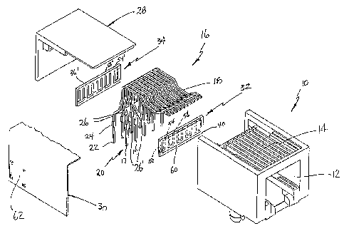
20 Referring now to the drawings, wherein like reference numerals represent
identical or corresponding parts throughout the several views, FIG. 1
illustrates an
exploded, perspective view of a first preferred embodiment of the present
invention.
11
__..~.~..._..._.,.....-,..._ _. . __._._.._. _ __......,_ .
i
CA 02291322 1999-11-30
Illustrated in FIG. 1 is a typical modular jack for mating a modular plug (not
shown) to a printed circuit board (PCB; not shown). Reference numeral 10
indicates generally a dielectric housing of the modular jack. Housing 10
includes a
plug-receiving opening 12 on the front side thereof which is sized to receive
a
mating modular plug (not shown). As described in any of my above-noted
patents,
the modular plug which mates with jack housing 10 normally includes a
plurality of
substantially planar, side-by-side contact terminals having an upper exposed
edge
which is adapted to mate with the spring contact portions of the jack, to be
to described in greater detail below.
Housing 10 is further provided on its top surface with a plurality of channels
14 which are adapted to receive a plurality of side-by-side electrical
conductors
indicated generally by reference numeral 16. There are ten such conductors
~5 illustrated in the embodiment of FIG. 1, but greater or fewer may be
provided, as is
well known.
Each of the conductors 16 include a spring contact portion 18 which is
designed to engage a correspondingly-spaced contact terminal in the mating
20 modular plug. The spring contact portions 18 are typically spaced 0.040"
from
each other.
12
T _ _. m~....-_. _ __...._...-..... ___ _ __ _ _ _..._w~..~.~.
CA 02291322 1999-11-30
i /_'
The other end of the conductors 16 terminate in a PCB-matable end portion
indicated generally by reference numeral 20. In the illustrated embodiment,
the
PCB-matable or end portions 20 are arranged in two rows in an alternating,
staggered array to fit through a standard PCB grid spacing. This typically
means that
the two rows of PCB-matable portions are separated by 0.100", and adjacent
conductors in the same row (e.g., conductors 17 and 19) are also separated by
0.100". For ease of reference throughout this specification, the end portions
20 of
the conductors which include conductors 17 and 19 will be referred to as the
front
row, while the other row of end portions will be referred to as the rear row.
to
As illustrated in FIG. 1, the PCB-matable end portions 20 comprise solder tail
portions 22 and tabs 24 for positioning the conductors 16 in slots (not shown)
located in the rear of housing 10.
However, it should be understood that alternate arrangements for end portions
are possible, including various well known surface mount tail arrangements.
Positioned above tabs 24 are intermediate portions 26 of conductors 16. In
the illustrated embodiment, five intermediate portions 26 are shown in the
rear row
20 of the end portions 20 of conductors 16, while five intermediate portions
26' are
illustrated in the front row of end portions 20 of conductors 16. It may be
13
CA 02291322 1999-11-30
appreciated that intermediate portions 26 and 26' are also arranged in an
alternating, staggered array.
The modular jack housing 10 preferably also includes a cap 28 that covers
conductors 16, and may also include a metal shield 30 for enclosing housing
10, for
a purpose to be described in greater detail hereinafter.
In accordance with the present invention, there is provided a first capacitor
module indicated generally by reference numeral 32 and a second capacitor
to module which is indicated generally by reference numeral 34. Modules 32 and
34
are substantially identical to each other and are aligned in parallel but on
opposite
sides of intermediate portions 26 and 26' of conductors 16. More particularly,
the
first capacitor module 32 faces and makes contact with intermediate portions
26' in
the front row of conductors, while the second capacitor module 34 faces and
makes
contact with the intermediate portions 26 in the rear row of conductors.
FIG. 2 illustrates an enlarged view of module 32 which is seen to comprise a
substrate 36 having a front side 38 and a back side 40 (not shown in FIG. 2).
On
front side 38 are etched or otherwise formed a plurality of (in this case
five) U-
2o shaped capacitor traces 42, 44, 46, 48 and S0. Each U-shaped trace, e.g.
trace 42,
includes one leg 52 which can be denominated the capacitor portion and another
leg 54 which can be denominated the copper trace portion. Copper trace portion
14
~__. _..._~,_...._ ._.___.___.._ .__..__....._.__..
CA 02291322 1999-11-30
54 is adapted to be connected to the intermediate portion 26' of conductor 16.
It
will be understood, however, that both legs 52 and 54 serve to define the
capacitor.
In a similar manner, trace 44 includes a capacitor portion 56 and a copper
trace
portion 58, while the same pattern holds for U-shaped traces 46, 48 and 50.
As shown better in FIG. 1, on the back side 40 of module 32 is formed a large
capacitor pad 60 which is connected to ground by means of shield 30 and its
integrally formed ground connections 62 so that any charge induced on the
relatively large plate or pad 60 is provided with a path to ground.
Connections 62
1o may be either soldered or crimped to pad 60.
As seen in FIG. 1, copper trace portions 54 and 58 are aligned with the first
two intermediate portions 26' of end portions 17 and 19 in the front row of
contacts
so as to be matable therewith. In a similar manner, copper trace portions 54'
and
~5 58' on the front face of the second substrate 36' are aligned with the
intermediate
portions 26 on the rear row of the end portions of conductors 16. Thus, each
capacitor on module 32 connects to every other conductor 16, while those
conductors not connected to the capacitors on substrate 32 are connected to
the
five capacitors on substrate 34. In this manner, greater surface area is
available on
20 each of the substrates 32 and 34 for providing the desired capacitances.
Use of
every other contact in this manner also eases the manufacturing tolerances
required.
__ .._~...~.~-_~ _ ___.... _..._.._.~...,w.._ ___~__.__... __._ _ .~..._..
CA 02291322 1999-11-30
~_1
In this manner, there is provided a capacitor in series with each of the
conductors 16. Thus, the signal on each conductor 16 will be filtered through
its
respective capacitor. The capacitance of each capacitor will be selected to
filter out
the noise.
The electrical connection of the capacitors to the intermediate portions of
the
conductors may be achieved by using either reflow solder techniques, by
melting a
fillet of solder previously placed on the conductor's intermediate portion, by
surface
contact to a conductive ink, or by other means well known in the art.
Regarding the substrate 36, it is desirable to choose a substrate that has a
particular, desired dielectric constant. The capacitance of each capacitor pad
will
depend upon the dielectric constant of the substrate, the thickness of the
substrate,
and the surface area of the capacitor ground plate and the pads. Also, the
material
is of the substrate may have to withstand the high temperature of reflow
solder
operations. The typical preferred materials for the substrate 36 include:
polyphenylenesulfide (PPS); polyselfone (PS); liquid crystal polymers;
polyketone;
or PCT polyester. The preferred thickness of the substrate range between
0.015"
and 0.035". The size of the capacitor pads are selected to achieve
capacitances
2o ranging between 100 and 1,200 picofarads for each conductor.
16
....._...._.._..~......._..T..... . ......... . ............__._.._
d.._._.__..__ .._ ... _... ._ .. . ...... .. ..
CA 02291322 1999-11-30
.\
It is preferred to use polymer substrates for the capacitor modules since they
have the ability to flex without stress failure, whereas less desirable
fiberglass
boards are rigid. Flexibility may be important in enabling the board to
accommodate slight differences in dimension to more easily engage the
intermediate portions of the conductors. Thus, a substrate with a slight
'give' may
be better able to achieve desired connection between the capacitor pad and the
conductor.
As seen in FIG. 3, a ferrite bar 64 may be bridged across all capacitors 42
to through 50 on substrate 36 to provide some additional filtering. The
ferrite bar aids
in dissipating some of the higher frequencies.
Referring now to FIG. 4, there is illustrated an alternate embodiment of the
present invention which differs from the first embodiment in the provision of
a
t5 single capacitor module 66 located entirely on one side of the intermediate
portions
of conductors 16. Capacitor module 66 includes all ten capacitors in one
module.
FIG. 5 illustrates module 66 in an exploded view which is seen to include a
first capacitor substrate 68, a second capacitor substrate 70, and a third or
insulating
2o substrate 72 placed between substrates 68 and 70 to electrically insulate
same.
17
....... .....T_ . ....._.........,~,..~.._....--..__.. ......~~~-
_...........___.._~_ ......__........m...._. .... ..... .... ._............
...
CA 02291322 1999-11-30
r ,
On the first substrate 68 are positioned five fingers 74, 76, 78, 80 and 82 on
the top surface 84 on which are deposited five capacitor traces 86, 88, 90, 92
and
94.
Note that each trace 86-94 includes a roll-over portion 96, 98, 100, 102 and
104 which extend over the outside vertical edge of respective fingers 74-82.
On
the reverse side of substrate 68 is positioned a large pad which serves as a
ground
plane (not shown).
1o The second substrate 70 has a bottom side 106 on which is positioned a
large
pad 108 that serves as a ground plane. The top side 110 of substrate 70 is
seen
better in FIG. 6 and includes five capacitor traces 112, 114, 116, 118 and
120.
Each of the five capacitor traces has a roll-over portion 122, 124, 126, 128
and 130
on its front face.
Referring back to FIG. 5, it is seen that fingers 74-82 fit between the
positions
of the roll-over portions 122-130, for reasons which will become clear
hereinafter.
Referring back to FIG. 4, the first two intermediate portions in the front row
of
2o end portions 20 have been labeled with reference numerals 23 and 27, while
the
first two intermediate portions in the rear row have been labeled with
references
numerals 21 and 25.
18
_ .._._.....?. _...._."~._.__. _.~."___ _ .... . ~_ . . _ ...._....-_ _~ .
CA 02291322 1999-11-30
o I_1
It may be appreciated from the foregoing that when assembled, roll-over
portion 96 of trace 86 on finger 74 electrically connects to intermediate
portion 21.
Similarly, rollover portion 130 of trace 120 mates with intermediate portion
23; roll-
over portion 98 (not shown in FIG. 4) of trace 88 mates with intermediate
portion
25; and roll-over portion 128 of trace 118 mates with intermediate portion 27.
The
connections just described with respect to the first four capacitors in
capacitor
module 66 hold for the remaining six capacitors in a similar manner. As
before, the
electrical connection may be by any of the previously described techniques.
Substrate 70 may also be provided with a ferrite bar 132 as illustrated in
FIG. 7 to
provide additional filtering, if desired.
Referring now to FIG. 8, a third preferred embodiment of the present
invention is illustrated, but, for the sake of simplicity, without the
housing, cap or
is shield members illustrated in the earlier embodiments. In addition to
conductors
16, FIG. 8 illustrates a first capacitor module 134 and a second capacitor
module
136. It is noted that capacitor modules 134 and 136, unlike the first
embodiment,
are not identical to one another, but are complimentary in the sense that in
use they
fit together, in a manner that will be described in greater detail
hereinafter.
The first capacitor module 134 is provided with a pair of wings 135 and 137
that fit in keyways in the connector housing (not shown) for alignment and
19
_._~_. _ ___.__~.._~.~....~..-.._. _ _..._._._. _. __ ..___.___.. _._,.-.
CA 02291322 1999-11-30
o ~ 1
installation purposes. The first module 134 further includes a plurality of
fingers
138, 140, 142, 144 and 146 extending in the opposite direction from wings 135
and 137. On the top surface of fingers 138-146 is positioned a large metallic
pad
150 that serves as a ground plane 150.
Referring now to FIG. 9, first capacitor module 134 includes a bottom surface
152. On each finger 138-146 of bottom surface 152 is positioned a capacitive
pad
154, 156, 158, 160 and 162. Each of the capacitive pads 154-162 include a roll-
over portion 164, 166, 168, 170 and 172 (see FIG. 10) for contacting the
1o intermediate portions of alternating conductors, as will be described in
greater
detail hereinafter.
Referring back to FIG. 9, positioned between capacitor pads 154-162 are
smaller capacitor pads 174, 176, 178, 180 and 182 each of which has a roll-
over
portion 184, 186, 188, 190 and 192, respectively (see FIG. 10) for contacting
the
intermediate portion of certain conductors.
Referring back to FIG. 8, the second capacitor module 136 includes a ground
plane 194 formed on the top surface thereof and a plurality of fingers 196,
198,
200, 202 and 204 extending forwardly therefrom.
CA 02291322 1999-11-30
o ~_1
As may be seen in FIG. 9, on the bottom surface 206 of fingers 196-204 are
deposited capacitor pads 208, 210, 212, 214 and 216 each of which has a roll-
over
portion 218, 220, 222, 224 and 226.
Roll-over portions 218-226, it may be appreciated, are aligned opposite to
rollover portions 184-194 of capacitor pads 174-182 on first substrate 134.
FIG. 11 illustrates the capacitor module 134 in an assembled condition with
the
second capacitor module 136 and the intermediate portions of the conductors 16
to positioned therebetween.
It may be appreciated from FIG. 14 that capacitor pad 154 is of sufficient
size to
serve as the capacitance for the conductor that includes intermediate portion
21.
However, due to the alternating, staggered array of conductors 16, under some
is circumstances there may not be enough room on the bottom surface of the
first
module 134 to provide sufficient surface area for the desired size capacitor
pad for
the conductor having intermediate portion 23. Thus, the capacitance for
intermediate portion 23 is provided by two pads, i.e., capacitor pad 174 on
first
module 134 and pad 216 on second module 136. The fact that both pads 174 and
20 216 are connected to intermediate portion 23 is also illustrated in FIG.
12.
21
T _.__~ _.. ~ ....~....-..._.__ _ __ ...... __... ... ..
CA 02291322 1999-11-30
.~ _ \
In a similar fashion, the capacitive pads for the rear row of contacts 21, 25,
29,
31 , etc., may be provided by the single capacitive pads on the first module
134,
such as capacitive pads 156, 158, etc. The capacitances for those conductors
in the
front row of contacts are provided by one pad on module 134 and another pad on
module 136 (e.g. pads 176 and 214 for intermediate portion 27). In this
manner,
sufficient space may be provided by both modules 134 and 136 to achieve the
desired capacitance.
Care must be taken not to unintentionally ground the intermediate portions of
to conductors 16. To this end, as seen in FIG. 10, a beveled edge 230 is
provided
adjacent each finger tip on first module 134 adjacent the ground plane and the
point of contact of each intermediate portion of the conductor. Further, as
also seen
in FIG. 10, a beveled edge 235 is provided between adjacent finger tips.
is Similarly, notches or beveled edges 240 (see FIG. 8) are formed on the
fingers
of the second module 136, as are beveled edges 245 between adjacent finger
tips.
As may be viewed in FIGS. 12 and 13, these notches or beveled edges 230,
235, 240 and 245 provide clearances to prevent the unintentional grounding of
the
2o intermediate portions 23 and 31 of conductors 16.
22
CA 02291322 1999-11-30
It may appreciated that I have provided a filtered modular jack which both
provides the desired capacitance and still meets the 1,000 volt dielectric
withstand
requirement imposed by the FCC. The split board capacitance feature allows
utilization of vacant space next to a single conductor as the capacitive pad
for the
adjacent conductor. In other words, the space between conductors is utilized
as the
capacitive pad for the neighbor. This allows a great increase in the size of
the pads,
which in turn enables a greater variation in the desired capacitance.
It should further be understood that the present invention may be utilized in
to any modular jack wherein the PCB mateable portions are arranged in an
alternating,
staggered array. Obviously, numerous modifications and variations of the
present
invention are possible in light of the above teachings. It should therefore be
understood that within the scope of the appended claims, the invention may be
practiced otherwise than as specifically described herein.
23