Note: Descriptions are shown in the official language in which they were submitted.
CA 02291455 2006-03-07
1
CONNECTOR LOCATING AND RETAINING DEVICE FOR PRINTED
WIRING BOARD APPLICATION
FIELD OF THE INVENTION
The present invention is related to electrical connectors. More particularly,
but not exclusively, the present invention is related to a device for
positioning and
securing an electrical connector to a printed wiring board.
BACKGROUND OF THE INVENTION
The present invention relates generally to improvements in electrical devices
intended for surface mounting on printed wiring boards and in the mounting
components thereof. Conventional mounting posts typically include hooked ends
that
are used to snap an electrical device into place on a printed wiring board.
However,
such mounting posts have many deficiencies. For example, when the hooked ends
of
the mounting posts of a board-mounted device snaps into engagement with the
underside of the board, the impact may cause other components to be jarred
loose.
Further conventional mounting components typically include separate elements
for
locating the electrical device and for retaining the device to the printed
wiring board.
An improvement over the hooked-end mounting post is described in U.S.
Patent No. 5,244,412, to Hatch et al., entitled "Electrical Device for Surface
Mounting on a Circuit Board and Mounting Component Thereof." The Hatch et al.
mounting device includes a pair of positioning posts and a molded mounting
post.
The position posts cooperate with corresponding openings in a printed wiring
board
to position the connector with respect to the board. The separately provided
mounting post includes a clip that forms tangs that extend beyond the sides of
the
post. When the connector employing the Hatch et al. mounting device is mounted
to
CA 02291455 2006-03-07
2
a printed wiring board, the tangs deflect within a receiving hole in the board
to retain
the connector on the board.
While the Hatch et al. device is an improvement over other conventional
mounting posts that mechanically connect devices to printed circuit boards,
the
Hatch et al. still presents problems in surface mount applications. The Hatch
et al.
device fails to address problems encountered when mounting electrical
connectors to
printed wiring boards that have components mounted to both sides of the board
as
the Hatch et al. mounting device protrudes through the board. Further, the
Hatch et
al. device does not provide for a reduced-sized connector as separate
positioning and
mounting posts are required to retain the connector on the board. It would,
therefore,
be desirable to reduce the space required by the retaining mechanism of an
electrical
connector. It is also desirable to have a retaining mechanism that reduces the
likelihood of interference with other components mounted to the printed wiring
board. The present invention provides such a solution.
SUMMARY OF THE INVENTION
More specifically, according to the present invention, there is provided an
electrical connector assembly, comprising:
an insulative housing having top and bottom walls, a rear wall, and opposed
lateral walls all defining an interior section, the insulative housing
comprising a
mounting post that extends from the bottom wall;
a plurality of conductors that extend into the interior section and extend
outward of the electrical connector;
an outer shield, this outer shield covering at least a portion of the top wall
and
the opposed lateral walls of the housing, the outer shield including an
engaging
section adapted to be received by the mounting post such that ends of the
engaging
section extend beyond a peripheral edge of the mounting post;
wherein the mounting post and the engaging section cooperate to align and
retain the electrical connector on a printed wiring board when mounted
thereto.
CA 02291455 2006-03-07
3
The present invention also relates to an electrical connector that includes an
insulative housing defining top and bottom walls, a rear wall and opposed
lateral
walls, the electrical connector having a plurality of conductors, and an outer
conductive shielding that covers at least the top, rear, and opposed lateral
walls, the
electrical conductor comprising:
a plurality of engaging sections that project from a bottom of the electrical
conductor and proximate the bottom wall; and
a plurality of mounting posts extending from the bottom, the mounting posts
defining a groove and an opening in a side of the mounting posts,
wherein the engaging sections are adapted to be disposed within respective
grooves of the mounting posts by passing through respective openings of the
mounting posts.
The present invention further relates to a modular jack connector, comprising:
a housing comprising a top wall, a bottom wall, a pair of opposed lateral
walls, and a rear wall;
generally cylindrical mounting posts formed on the bottom wall, the
mounting posts each defining a groove that extends across a diameter of the
mounting post, the mounting posts further defining a generally U-shaped
opening
formed in a cylindrical wall, the U-shaped opening faces outwardly of the
modular
jack connector;
a conductive outer shielding that surrounds the top wall, the pair of opposed
lateral walls, and the rear wall, the conductive outer shielding including
generally T-
shaped sections extending from a bottom of said outer shielding,
wherein the "T-shaped" sections are disposed in the "U-shaped" openings of
the mounting posts such that a top of the "T-shaped" sections are held in
respective
grooves when the conductive outer shielding is secured to the housing.
According to other non-restrictive illustrative embodiments of the present
invention:
CA 02291455 2006-03-07
3a
- The electrical connector may be surface mounted to a circuit board that
includes
an insulative housing, an outer shielding, and mounting posts formed at a base
of
the insulative housing.
- The "T-shaped" sections are bent at approximately a 90° angle with
respect to the
lateral walls of the housing and through the opening in the mounting posts
such
that the top of "T" is retained within the groove that is formed in the bottom
of
each mounting post.
- The top of the "T" has length that is longer than the diameter of the
mounting
post such that the ends of the "T" extend beyond the periphery of the mounting
post, and are longer than the diameter of a receiving hole of a printed wiring
board into which the mounting post is inserted. When the connector is mounted
to a printed wiring board, the mounting posts are inserted into their
respective
receiving holes and the ends of the "T" that extend beyond the periphery of
the
mounting posts are deflected upwardly in a direction opposite of the direction
of
insertion to retain the connector on the printed wiring board.
- The length of the mounting post is less than the width of the printed
circuit board
to which the connector is mounted. This advantageously provides for a
connector
that may be mounted to one side of the board without interfering with
components mounted on the other side of the board.
The foregoing and other objects, advantages and features of the present
invention will become more apparent upon reading of the following non-
restrictive
description of an illustrative embodiment thereof, given by way of example
only with
reference to the accompanying drawings.
BRIEF DESCRIPTION OF THE DRAWINGS
In the appended drawings;
Figure 1 is an elevational view of a front of an electrical connector
according
to the present invention;
CA 02291455 2006-03-07
3b
Figure 2 is an elevational view of a side of the electrical connector
according
to the present invention;
Figure 3 is an elevational view of a rear of the electrical connector
according
to the present invention;
Figure 4 is an elevational view of a bottom of the electrical connector
according to the present invention;
Figures SA and SB are cross-sectional views illustrating the electrical
connector according to the present invention mounted to a printed wiring
board; and
Figure SC is a partial elevational view illustrating the electrical connector
according to the present invention mounted to a printed wiring board as viewed
from
the underside of the printed wiring board.
DETAILED DESCRIPTION OF THE PREFERRED EMBODIMENTS
The present invention has applicability to connectors that are surface mounted
to a printed wiring board. Referring to Figures 1-4, there is illustrated a
modular jack
connector (electrical connector) 10 having a housing 11 comprising a top wall
12, a
bottom wall 14, a pair of opposed lateral walls 16 and 18, and a rear wall 19.
The
housing 11 is constructed of a thermoplastic polymer having suitable
insulative
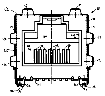
2~
properties. Within these walls is an interior section 20, which has a forward
open end
CA 02291455 1999-12-02
BERG2469/d519 'US - 4 - PATENT
the bottom wall 14 in this interior section 20 there is a medial wall
generally shown at
numeral 26 which has a rear side 28 and a front side shown generally at
numeral 30. Formed
on the oottom: wall 1~4. are generally cylindrical mounting posts 32 having
ends 34. Each
mounting post 32, at each end 34, defines a groove 36 that runs .across a
diameter of the
mounting post 32. A generally "U-shaped" opening 38 is also formed in the
cylindrical wall
of the mounting post 32 and faces outwardly of the connector 10. As will be
explained later,
the mounting posts 32 are provided as part of an improved device to both
locate and secure
the electrical connector l0 to a printed wiring board.52 (see, Figures 5A-5C).
Within the housing 11 is disposed a plurality of conductive leads 48, which
are adapted to mate with complementary leads of a plug (not shown). The
conductive leads
48 extend into the interior section 20 and run downward to the medial wall 26
and along the
bottom of the electrical conductor 10. The conductive~leads extend outward of
the rear of the
electrical conductor 10 to formpad-engaging contact portions 50. As the
electrical connector
10 is mounted to the printed wiring board, the contact .portions 50 touch a
solder paste
composition on contact pads on the printed wiring board. Later, the contact
portions 50 may
be permanently soldered to the board using conventional means (e.g., reflow).
Surrounding the top wall 12, the.pair:of opposed-lateral walls 16 and 18, and
the rear wall 19 of the housing 11 is a conductive outer shielding 40. A
plurality of tabs 42
proj ect from the outer shielding 40 and extend from the front toward the rear
of the connector
10. The tabs 42 are provided to contact a chassis of the electrical device
(e.g., a personal
computer) within which the electrical connector 10 is mounted in order to
reduce
electromagnetic emissions by grounding the outer shielding 40 to the chassis.
As best
illustrated by Figure 4, two generally "T-shaped" sections 44 are provided at
the bottom of
the outer shielding 40. The "T-shaped" sections 44 are belt into the "U-
shaped" opening 38
of the mounting posts 32 such that the top of the "T-shaped" section 44 is
held in the groove
36 when the outer shielding 40 is secured to the housing 11. As illustrated in
Figure 2, ends
46 of the top portion of the "T-shaped" section 44 extend beyond the outer
periphery of the
mounting post 32.
As will be appreciated by those skilled in the art and will be further
explained
hereafter with reference to Figures 5A-5C, the electrical connector 10 may be
mounted the
- printed wiring board 52 by press-fitting. The printed wiring board 52
defines a hole 54 into
CA 02291455 1999-12-02
BERG2469/4519.US - 5 - PATENT
which the mounting post 32 is inserted. The hole 54 is larger in diameter than
the mounting
post 32, but smaller in diameter than the length of the top of the "T-shaped"
section 44 (as
defined by a length between the edges of ends 46). -Further, the mounting post
32 preferably
has a length that is shorter than the thickness of the printed wiring board
52, such that the
mounting post 32 does not protrude beyond the underside of the board 52 when
the connector
is mounted to the top side. In order to achieve this in a typical application
where the
printed wiring board has a thickness of 0.06210.007 inches, it is preferable
that the mounting
posts 32 have maximum length of 0.055 inches. As shown in Figure 5A; when the
electrical
connector 10 is pressed into the printed wiring board 52 for mounting, the
ends 46 deflect in
10 a direction opposite that of -the direction of insertion. The biasing force
created by the
deflected ends 46 maintains the electrical connector 10 in the mounted
position with respect
to the printed wiring board 52. The biasing force is preferably large enough
such that the
electrical connector 10 will remain on the board 52 when the board 52 is
turned upside-down,
or such that the connector 10 remains on the board 52 when other components
are mounted
(i.e., able to withstand any shocks associated with the mounting of other
components).
As can be appreciated by those of skill in the art, the present invention
provides for an improved device for mounting an electrical connector to a
printed wiring
board. In particular, the present invention provides for a mounting apparatus
that both
positions and retains the connector on the board, thus eliminating the
necessity of the prior
art which requires separate positioning and retention mechanisms. Further, the
present
invention provides for high retention forces while necessitating only a
relatively short hold
down component.
Further, while only two mounting posts have been illustrated in the figures,
it is within the scope of the present invention to provide more than two
mounting posts to
position and secure the electrical connector. It may be desirable to provide
more than two
mounting posts when the electrical connector is relatively large or heavy. In
addition, while
the mounting posts have been illustrated as accepting the "T-shaped" sections
that are formed
as part of the outer shielding, the mounting posts may be formed having a
metal strip (or
other semi-rigid material) embedded therein. In this alternative, the length
of the embedded
strip would longer than a diameter of the mounting posts in order to form the
ends 46. The
outer shield, thus, would not require the "T-shaped" sections.
CA 02291455 1999-12-02
t....r
BERG2469/451'9 US - 6 - PATENT
The present invention may be employed in other specific forms without
departing from the spirit or essential attributes thereof. For example, any
number of materials
may be used in manufacturing the disclosed latch member. While the invention
has been
described and illustrated with reference to specific embodiments, those
skilled in the art will
recognize that modification andvariations may be made without departing from
the principles
of the invention as described herein above and set forth in the following
claims.
. . . . .r
. . . . . :."::~ - _ . .. .._ ~:~~~.. " .. . ~ .. ~ w . ,