Note: Descriptions are shown in the official language in which they were submitted.
CA 02291917 1999-12-07
Chand 10-10-21-8 1
OPTICAL COMMUNICATION SYSTEM COMBINING BOTH BASEBAND AND
' PASSBAND SIGNALS
Cross Reference To Related Applications
This application claims the benefit of United States Provisional
application Serial No. 60/112,480 filed by the present applicants on December
12, 1998.
Field Of The Invention
i
This invention relates to optical communication systems and, in
particular, to an optical communication system which transmits both baseband
signals and passband signals over a common optical fiber.
Background Of The Invention
An ever increasing communication need of today is to deliver
multimedia services such as voice, data, high speed Internet access, video
conferencing, video on demand, and broadcast television video to small
businesses and residences. Cost is the prominent issue for the deployment of
such networks. Among various technologies that are currently available and
being deployed, optical fiber extending to users -- Fiber to the Home (FTTH) --
is the preferred technology to meet present and future needs. Service
providers are taking fiber as deep into their networks as their costs allow.
Two different optical fiber communication systems have evolved for
carrying information to homes and businesses. One system delivers
information by a digitally modulated series of light pulses. These are
referred
to as baseband signals. A second system uses a plurality of frequency
separated carriers. Each carrier is modulated to transmit a higher order
digital
signal. These are passband signals. Each system has its own specialized
equipment, its own physical plant and its own standards.
CA 02291917 1999-12-07
Chand 10-10-21-8 2
Fig. 1A schematically illustrates a baseband system 10 comprising a
- central office 11 providing optical fiber connections to a plurality of
homes 12
and businesses 13. High power optical aignals at single or multiple
wavelengths are transmitted over a plurality of access fibers 15A, 15B, 15C to
respective optical power splitters and/or wavelength demultiplexers 16A, 16B,
16C, and at each powe't splitter or demultiplexer, e.g., 16B, the high power
signal is divided into a plurality of lower power or separate wavelength
signals
and transmitted over a respective plurality of end user fibers 17A and 17B.
These signals are called downstream signals. The downstream signals are
l0 typically a digitally modulated baseband series of light pulses centered in
the
1.3 - 1.6 p,m wavelength band. Signals from the end users to the central
office, called upstream signals, are typically digitally modulated baseband
pulses in the same 1.3 - 1.6 wavelength band but at different wavelength from
the downstream wavelength are transmitted in the reverse direction over the
same fibers. The upstream signals can be buffered and time division
multiplexed for burst transmission at the power splitters, e.g., 16B. Since
this
system does not employ any active electronic or photonic component between
the central office and the users, it is called a Passive Optical Network
(PON).
Fig. 1 B illustrates a simplified baseband modulation scheme. Typically
a digital 1 is represented by a light pulse in the series. A digital 0, by the
absence of a pulse in a pulse position. Alternatively, the signal can be
inverted
with a pulse representing digital 0 and its absence representing 1.
Fig. 2A schematically illustrates a passband system 20 comprising a hub
21, and a plurality of fibers 22A, 22B, 22C connecting the hub to a respective
plurality of fiber nodes 23A, 23B and 23C. Each node is connected, as by a
plurality of fibers or coaxial cables 24A and 24B to a plurality of homes 12
and
businesses 13.
Fig. 2B illustrates the radio frequency spectrum of a typical digitally
modulated passband signal. The signal comprises a plurality of different radio
CA 02291917 1999-12-07
Chand 10-10-21-8 3
frequency (RF) carriers spaced apart in frequency (e.g. 6 MHz spacing in the
NTSC system). Each of the carriers is modulated among a plurality of states to
carry a higher order digital signal to encode plural bits for each modulation
state. The modulation can be amplitude modulation, frequency modulation,
phase modulation or a combination of them.
,,
Digital passband signals are conventionally transmitted using two RF
carriers that are frequency~locked but 90 degrees out of phase. The two
carriers are said to be in quadrature. The two carriers are separately
amplitude
modulated (AM), and the modulated carriers are combined to form a single RF
output having both amplitude information corresponding to their vector sum and
phase information corresponding to their vector angle. The technique is known
as quadrature amplitude modulation or QAM.
Fig. 2C illustrates the simplest case of QAM which occurs when each of
the carriers has only two states (e.g. +V and -V). One carrier, is considered
the
reference carrier and is called the in-phase channel. It's amplitude is
represented along the vertical axis of Fig. 2(C). The other carrier,
90° out of
phase, is called the quadrature channel. Its amplitude is represented along
the
horizontal axis. As can be seen from the diagram, if each carrier has two
states (+V, -V), then there are four possible combined outputs, each of which
can represent two bits of information: (0,0), (0,1), (1,0), (1,1). This simple
modulation scheme is known as quadrature phase shift keying (QPSK).
Similar modulation schemes can be based on amplitude modulation of
the carriers among a larger number of states. For example if both carriers can
be modulated among four amplitudes, the combined output can represent 4 x 4
= 16 states, and the modulation is called 16 QAM modulation. Modulation
using 8 x 8 = 64 states is 64 CTAM.
In the past few years there has been an international effort from service
providers and system manufacturers to define common specifications aimed at
CA 02291917 1999-12-07
Chand 10-10-21-8
the extension of fiber all the way to homes and businesses to deliver existing
and future services. These specifications are now part of International
Telecommunication Union (ITU) standard 6.983.1
According to 6.983.1, all services are transported in baseband format in
both the upstream and downstream directions on a power splitter-based
system. In one variant of the network, a shared 155-Mbps baseband signal is
transported downstream irk the 1.5-gm band and the same bit rate is sent
upstream in the 1.3-~m band on a single fiber. For low cost, a single
transmitter in the central office and a single fiber can serve up to 32 users
if the
fiber is all the way to the user's premises. The number of users can even be
greater if the receiver is at the curb and electrical signals are distributed
to
multiple dwellings. The 6.983.1 specification calls for a minimum logical
reach
of at least 20 km and an optical power budget consistent with that reach. The
specified downstream receiver sensitivity at a bit error ratio of <10'°
is -30 dBm
for Class B operation and -33 dBm for Class C.
A downstream capacity of 155 Mbps shared among 32 end users is
more than adequate for interactive services such as voice, data, or
interactive
video, but can be quickly exhausted by multichannel broadcast video,
especially if high definition TV (HDTV) is to be delivered. One approach to
dealing with broadcast video delivery in 6983.1 is to increase the downstream
bandwidth from 155 to 622 Mbps. This approach is very expensive and
complicates video channel switching. Alternatively video signals can be
delivered on a separate fiber using a separate transmitter and a separate
receiver. This approach is even more expensive. Accordingly there is a need
for a new approach to deliver multimedia services to small businesses and
residences.
CA 02291917 1999-12-07
Chand 10-10-21-8 5
Summary Of The Invention
This invention is a new communication system in which multichannel
broadcast digital services are distributed to each user with the broadcast
video
signal riding in the passband above a digital baseband 155-Mbps signal. The
system can deliver more'than 1 Gbps additional bandwidth to each subscriber.
The passband bandwidth will accommodate growth in downstream services
including video on demancJ~ higher speed web downloads including improved
streaming audio and video, HDTV, interactive video, and personalized video.
The invention requires only a single transmitter, a single transmission fiber
and
a single optical receiver for each user or group of users. A single
transmitter,
single fiber, single optical receiver system is much less expensive than two
systems, one transmitting baseband and the other passband. A single receiver
is greatly cost beneficial to achieving economical fiber to the home.
Although the result of the invention is to add digital video and other
bandwidth demanding services on the system described in 6983.1, it can also
be used in other architectures where specifications or requirements differ
from
6983.1. For example, upstream or downstream data rate and optical
wavelengths and the required receiver sensitivity and bit error rates may be
different. The invention can also be used in point to point transmission of
baseband and passband signals on a single fiber using single transmitter and
receiver. Furthermore, the optical receiver or ONT does not have to be at the
customer premises. It can be outside on the curb and from where baseband
and passband services can be delivered to subscribers sharing that ONT on
twisted copper wires or coaxial cables, in an architecture popularly known as
Fiber to the Curb (FTTC). For twisted copper wires, the services can be
delivered using any of the conventional digital subscriber line techniques.
For
coaxial lines, hybrid fiber coaxial (HFC) technology is used.
In an exemplary embodiment, an optical communication system
comprises a diplexer for electronically combining the baseband and passband
CA 02291917 1999-12-07
Chand 10-10-21-8 6
signals, a digital laser transmitter for generating an optical signal
containing the
combined signals, a length of optical transmission fiber for transmitting the
optical signal, and, for each user or group of users, an optical receiver
optically
coupled to the fiber.
Brief Description Of TMe Drawings
The advantages, nature and various additional features of the invention
will appear more fully upon consideration of the illustrative embodiments
described in connection with the accompanying drawings. In the drawings:
Figs. 1 A and 1 B illustrate features of a baseband communication
system;
Figs. 2A, 2B and 2C illustrate features of a passband communication
system;
Fig. 3 is a schematic block diagram of an optical communication system
combining both baseband and passband signals;
Figs. 4A, 4B and 4C are interrelated graphical representations useful in
explaining the operation of the transmitter in the system of Fig. 3.
Fig. 5 is a schematic diagram of an end user receiver for the system of
Fig. 3;
Fig. 6 is a diagram of a test system combining both baseband and
passband signals; and
Figs. 7-12 are graphical illustrations showing the results of tests using
the system of Fig. 6.
It is to be understood that these drawings are for purposes of illustrating
the concepts of the invention and, except for the graphs, are not to scale.
CA 02291917 1999-12-07
Chand 10-10-21-8 7
Detailed Description
Figures 1 and 2, which relate to conventional baseband and
conventional passband systems were described in the Background of the
Invention.
Fig. 3 is a schematic block diagram of an exemplary optical
communication system 30 for transmitting both baseband signals and
i
passband signals on one or more common optical transmission fibers 32. In
essence, the system 30 comprises an electrical combiner such as a diplexer 29
' which receives an electrical baseband signal from a baseband source 27 and
an electrical passband signal from a passband source 28. The diplexer 29
combines these signals in such a manner that there is no frequency
overlapping of baseband and passband signals. It produces a combined
electrical output signal containing the information of both input signals and
presents this combined electrical signal to a laser transmitter 31, preferably
a
semiconductor digital laser such as a distributed feedback (DFB) laser.
The transmitter 31 generates an optical output signal containing the
information of both the input baseband and the input passband. The optical
output signal is transmitted on one or more optical transmission fibers 32 to
the
inputs of one or more optical power splitters 33. Each power splitter 33
essentially splits the transmitted signal into a plurality of spectrally
similar
optical signals (which may be of lower optical power) and outputs these
similar
signals onto a plurality of end user fibers 34 for transmission to respective
optical receivers 35 either at the premises of end users or nearby (at the
curb).
At least one optical receiver 35 can detect and demodulate both the baseband
signals and the passband signals impressed on the incoming light. Thus a
single transmitter, single fiber path and a single optical receiver can
service a
single user (FTTH) or group of users (FTTC).
CA 02291917 1999-12-07
Chand 10-10-21-8 g
Figs. 4A, 4B and 4C are interrelated graphical representations useful in
explaining the operation of the transmitter 31 in the system of Fig. 3. Fig.
3A is
a qualitative graph of the light output versus current characteristic of the
laser.
This characteristic includes a linear region A-A' where the light output is
proportional to the current input.
Fig. 4B is a qualitative graph of the current produced as a function of
time for the combined sig~xal from the diplexer 29. The baseband signals B are
identifiable as abrupt current changes at a constant repetition rate. The
passband signals P are lower amplitude oscillations between baseband
changes. The laser transmitter 31 should be biased, as shown in Fig. 4A so
that the range of currents produced by the combined signal falls within the
linear region A-A' of the laser.
Fig. 4C qualitatively illustrates the response of laser transmitter 31 to
current produced by the combined signal from the diplexer 29. As can be seen,
the light output scales the current input.
It is contemplated that the transmitter 31 will be located at a central
office and the end-user receivers 35 may advantageously include local optical
transmitters for transmitting information upstream from the end-user to the
central office, in a manner similar to that used in conventional baseband
systems.
Fig. 5 schematically illustrates an advantageous optical receiving
arrangement 35 for end users. The arrangement comprises an optical
multiplexer 50 for receiving the transmitted combined optical signal from an
end
user fiber 34. The combined signal is applied to a receiving element 51, such
as a PIN diode, and the resulting combined electrical signal is fed into a
preamplifier 52. The preamplified combined electrical signal is then split by
diplexer 53 into its baseband portion and its passband portion.
CA 02291917 1999-12-07
Chand 10-10-21-8 g
In one embodiment of the system 30, the baseband signal is a digitally
modulated time division multiplexed (TDM) 155 Mbps baseband signal
conforming to the power budgets and other specifications of the ITU industry
standard 6.983.1. The passband signal is a quadrature phase-shift keying
(QPSK) frequency division multiplexed (FDM) greater than 1 Gbps passband
signal. The optical transmitter 31 combines the electrical input signals in a
diplexer, and the combined electrical signal is converted to an optical signal
by
a 1.55 ~,m DFB ~,m dig t I laser do biased above threshold. The optical
transmission fiber 32 is a conventional single mode fiber. The optical power
splitter can be a 1 x 32 splitter, and the end user optical-to-electrical
receivers
35 can comprise PIN diode receivers or APD receivers.
The invention may now be better understood by consideration of the
following specific examples and tests. In the examples and tests, which are
intended for those skilled in the art, the acronyms used are expanded when
they are first used and in the definitions section at the end of this
application.
The following examples are provided for the purpose of illustration only. The
examples should not be construed as limiting the invention.
Example
This example is to demonstrate this invention's feasibility. The
experimental detail combined with the description above shows advantages of
various possible components and methods.
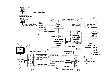
Fig. 6 schematically illustrates the test apparatus wherein a passband
signal derived from signals received by satellite dishes 60 and 61 and a
baseband signal from a transmitter 62 are electronically combined in diplexer
40. The combined electrical signal is converted to an optical signal by laser
transmitter 41, and the resulting optical signal is transmitted over a common
fiber 32 to a power splitter 33. An arm of the splitter transmits a portion of
the
received optical signal to an optical-to-electrical (O/E) receiver 35. The
CA 02291917 1999-12-07
Chand 10-10-21-8 10
resulting electrical signal is ultimately used to provide video display in a
TV 64.
Electrical circuitry pertinent to the particular passband signal used and to
the
tests conducted (but not to actual systems using the invention) will be
described in connection with these tests.
To minimize the' power budget requirements to approximate power
budgets of 6.983.1, QPSK modulation of the passband signal was used.
QPSK requires the least signal-to-noise ratio (SNR) compared to other higher
order quadrature amplitude modulation (M-QAM) or vestigial sideband
modulation (VSB). An avalanche photodetector (APD) receiver may allow
operation at 16-QAM. Required sensitivity for PIN diode based receivers may
need QPSK. The passband RF carriers can be modulated digitally with video,
data and audio baseband signals.
For demonstrating transmission of a passband QPSK signal with > 1
Gbps transmission capacity, a signal from the Hughes (Direct TV) Digital
Satellite Service (DSS) was used. The DSS signal delivers 150-200
MPEG2/QPSK channels (3-6 Mbps bandwidth per channel depending on the
motion content) multiplexed in two orthogonal circular polarizations in the
same
frequency range of 950 - 1450 MHz after the low noise block converter (LNB) in
the 46 cm diameter satellite dish. Each polarization has 16 digital carriers
using FDM with ~30 MHz separation and 24 MHz bandwidth per carrier. Each
carrier delivers ~ 40 Mbps payload, and thus a total throughput of 1.28 Gbps
is
delivered. The DSS uses concatenated Reed-Solomon and convolutional
forward error correction (FEC) codes for a coding gain of ~ 8 to 9 dBe.
By down-converting one polarity (e.g. the signal from dish 61 ) from 950-
1450 MHz to 270-770 MHz in down converter 65 and multiplexing it with the
other polarity, in 950-1450 MHz in combiner 66, a digital video signal was
built
that delivers all of the DSS standard channels within 270-1450 MHz including
an unused 770-950 MHz. The range of 270-770 MHz was used in the
experimental set up because of commercially available down-converters and
CA 02291917 1999-12-07
Chand 10-10-21-8 11
up-converters for this frequency range. In the unused RF spectrum, a QPSK
modulated rf test-signal centered at 860 MHz was added by transmitter 67.
The test-signal was generated with a ~QPSK satellite modem. A Fireberd
6000A communication analyzer was used for BER tests. A pseudorandom data
stream was used with q pattern length of 2z3-1 at a speed of 8 Mbps from the
analyzer to the QPSK modem producing a modulated signal centered at 70
MHz which was then up-converted to a frequency of 860 MHz. The QPSK
modem allowed turning o f of any FEC coding or to apply convolutional coding
with a Viterbi decoder with or without Reed - Solomon (R-S) block coding. To
keep the overhead bits to a minimum, the transmission was tested with no
coding, and 7/8 convolutional coding with or without (110,96) R-S coding. The
8 Mbps data rate with both 7/8 convolutional and (110,96) R-S coding results
in
a total bit rate of ~ 10.5 Mbps (i.e., 31 % overhead) and occupies less than 6
MHz bandwidth with QPSK modulation. This allowed use of 6 MHz standard
bandpass filters that are used for analog video channels. The total RF power
of the FDM video including the QPSK test-signal at the input to the diplexer
was 4.3 dBm or 2.7 mW. When this power drives a 50-S2 load, the peak-to-
peak current swing was 21 mA. The multiplexed and modulated signal is
converted into an optical signal by laser transmitter 41.
The FDM video passband signal was multiplexed with a 155.52 Mbps
pseudorandom NRZ baseband data stream of a pattern length of 2z3-1 through
diplexer 40. The peak-to-peak amplitude of the data pulses was 1.5V or 30mA.
This stream is equivalent to the time division multiplexed (TDM) baseband
signal used in 6.983.1, modulated at baseband and will be referred to as the
baseband or TDM signal. The baseband and passband signals were
multiplexed using diplexer 40. The advantages of using a diplexer instead of a
power combiner are negligible cross talk (-60 dBe) between the baseband and
passband signals and low insertion loss (~0.5 dBe) for each signal.
CA 02291917 1999-12-07
Chand 10-10-21-8 12
The composite baseband TDM and .passband FDM signal was then
used in E/O transmitter 41 to directly modulate a 1.55 ~.m DFB digital laser
after biasing it with a do current above its threshold current of 15.5 mA. No
thermoelectric cooling of the laser was used. As expected, the measured
system performance wad found to be very sensitive to the laser bias conditions
and the power levels of TDM data and FDM video signals. They affect the
extinction ratio, r, for baseband data, and the optical modulation index, m.
(Extinction ratio is defined as the ratio of average optical powers in the NRZ
l-
and 0- bits. The optical modulation index (OMI) is defined as the ratio of the
optical modulated signal power and the average optical power for passband.)
The laser bias affects the transmission of both baseband TDM data and
passband FDM video signals. Less than optimum bias current reduces the
swing between logic 1- and 0- bits, and introduces laser turn on delay and
clipping to distort the waveforms. Too much bias current reduces both
extinction ratio r and modulation index m for baseband and passband signals,
respectively. This reduces SNR and thus impairs the sensitivity of the O/E
receiver for both types of signals. Thus, an optimum laser bias is important
for
optimum system performance.
Based on the laser type and considering the levels of baseband and
passband signals, for their simultaneous transmission a bias current of 56 mA
was used. For bias >56 mA, the performance of both signals degrades. For
bias <56 mA the performance of baseband improves but that of passband
degrades. Without passband i.e., for baseband only, the laser bias was
reduced to 45.5 mA for optimum pertormance. Without baseband i.e., for
passband only, the bias current was reduced to 30 mA. At 56 mA, the
baseband extinction ratio was 6 dB instead of the desired > 10 dB in ITU-T
6.983.1. This results in a 1-dBo optical power penalty in receiver sensitivity
given by:
CA 02291917 1999-12-07
Chand 10-10-21-8 13
' OP(dBo) =1 OLog r + 1 . (,1 )
r-1
The SNR that determines the BER for a RF carrier is related to m and mean
square photocurrent (IPh) by:
(ml Ph ) 2
SNR= (2)
2Be~. (n,h z + Zql yH + I Ph Z RIN)
Here, Beff is the effective carrier bandwidth, n~h is the receiver thermal
noise
current presented to the preamplifier (typically 5 to 10 pA/~IHz). RIN is the
transmitter relative intensity noise in dB/Hz and q is the electron charge.
The
first term in the denominator is the thermal noise and the second term is the
shot noise of the receiver. For modern DFB lasers, the RIN of the transmitter
is
insignificant compared to the thermal noise and shot noise. IPh is
proportional
to the received optical power (PoP) at the receiver. From (2), gaining or
losing 1
dBo optical power is equivalent to gaining or losing 2 dBe in electrical SNR.
From (2), m should be as large as possible to increase receiver sensitivity.
The optical signal from the laser was coupled into a passive optical
network (PON) that consists of 20-km long conventional single mode fiber 32
and a 1x32 optical power splitter 33. A ~7 dB attenuation was measured
through the fiber and a total of ~16 dB insertion loss through the power
splitters
resulted in a total path loss of 23 dB between the transmitter and the
receiver.
Using an optical attenuator 68 just before the receiver 35, additional path
loss
could be introduced to vary the optical input power to the 0/E receiver 35.
A Lucent Microelectronics 1319 0/E receiver was used in two versions.
One O/E receiver had a PIN diode detector and the other had an APD detector.
The receiver. is designed to operate at a data rate of 2.5 Gbps. It has a 3 dB
bandwidth of 1.6 GHz and is rated for a 2.5 Gbps system sensitivity of ~ -24.5
dBm with PIN diode and ~ -33 dBm with APD at 10-'° BER. The TDM data
and
FDM video signals were separated from the output of the receiver 35 using a
CA 02291917 1999-12-07
Chand 10-10-21-8 14
- diplexer 69 identical to the diplexer 40 used to combine these signals at
the
transmitter side.
The TDM baseband signal was examined for eye diagram and BER. For
BER, the TDM signal was amplified and filtered through an SDH filter. The
passband signal was sf~udied for (i) SNR on a spectrum analyzer, (ii) live TV
reception on a TV set using a DSS set top box 71, and (iii) BER measurement
on 860 MHz QPSK test-signal.
For TV reception, the two polarities in 270-770 MHz and 950-1450 MHz
bands were separated using another diplexer 72. The 270-770 MHz band was
l0 upconverted via block up converter 73 to the original 950-1450 MHz. The
signals of two video polarities were then coupled to the DSS set top box 71
(STB) through a switch 74 controlled by the voltage from the STB. Depending
upon the 13 or 18 V DC received from the STB, the switch connected the STB
to the corresponding polarity. For the bit error rate measurements on the
QPSK test-channel, the video signal went through a 6 MHz bandpass filter
tuned to 860 MHz center frequency followed by amplification and down-
conversion to 70 MHz which was then demodulated and sent to the QPSK
modem 67 for bit error rate measurement.
Some subscribers may not be interested in passband services like
video. They may like to subscribe to baseband data only and use less
expensive baseband only ONU. To study the compatibility with baseband only
ONU and to estimate the optical power penalty for using a wide bandwidth
receiver for low speed data, a Lucent Microelectronics # 1330 integrated
receiver was also used. This is a complete receiver and includes alarm, data
and clock recovery circuits. This receiver is optimized for a data rate of
155.52
Mbps. Because of its limited bandwidth, model 1330 could be used only to
receive the baseband data with a total loss of video signal.
CA 02291917 1999-12-07
Chand 10-10-21-8 15
Figs. 7 shows RF spectra of baseband TDM and passband FDM at the
output of the PIN diode receiver 1319 for various received optical input
powers.
Curves 1, 2 and 3 show the spectra for input powers -20, -28 and -32 dBm,
respectively. Curve 3 also shows the thermal noise of the receiver that was
measured by turning off the optical input power to the receiver because then
shot noise and RIN are zero.
Figure 8 shows the'similar RF spectra for the APD receiver for -30, -34
and -38 dBm received optical powers. The spectra at -20 dBm in Fig.7 and at
-30 dBm in Fig. 8 are almost identical to that at the headend and thus our
optical system did not introduce any distortion. By viewing the DSS channels
on TV, we find that the integrity of the picture is not degraded for the SNR
>_
6dBe. We attribute this to the FEC used by DSS which gives about 9-dBe gain.
For SNR< 6 dBe, there are initially squares or tiles on images followed by a
total freeze or loss of the picture as expected from a digital TV signal. All
DSS
digital carriers < 1 GHz had the SNR ~ 6 dBe for PoP as small as -32 dBm for
PIN diode receiver and -38 dBm for APD receiver. With further reduction of
PoP, the SNRs are degraded by the receiver thermal noise.
To study the effect of the presence of baseband TDM signal on the SNR
of the passband FDM carriers, the SNR of 975 MHz carrier as a function of
received optical power is plotted in Fig. 9. Data are presented for both PIN
diode and APD based receivers with and without the presence of the TDM
data. For the video only transmission (i.e., without baseband data), the laser
bias current was reduced from 56 mA to a more optimum value of 30 mA to
increase OMI. Figure 9 suggests that there is an optical power penalty of ~2
dBo in video transmission due to the reduction of OMI in presence of baseband
TDM data. Nevertheless, with APD receiver we are able to deliver all the video
channels with >1 Gbps throughput at class C power level with 5 dB power
margin. With PIN diode receiver, system operates in class B mode as defined
CA 02291917 1999-12-07
Chand 10-10-21-8 16
in 6983 with a power margin of 2 dB or 4 dB.depending upon if the receiver is
considered a 155 or 622 Mbps receiver, respectively.
Figs. 10 and 11 show the measured BER as a function of received
optical power for the passband FDM and baseband TDM for both PIN diode
and APD based receiver's, respectively. For the FDM video test-channel, data
are plotted with and without FEC coding. For video the sensitivity of APD
receiver is 7 to 9dBo greater than of PIN diode receiver. For both receivers,
at
10-'° BER a marked improvement in receiver sensitivity (>2.5 dBo for
PIN and
>3.5 dBo for APD receiver) is observed when the 7/8 convolutional coding with
Viterbi decoder is used. For both receivers, sensitivity improves further by
>2.5
dBo with (110,96) Reed-Solomon coding resulting in a total coding gain of >5
dBo for PIN diode receiver and >6 dBo for APD receiver. With both convolution
and Reed-Solomon FEC coding, the 10-'° BER sensitivities are -30.3 dBm
and
-39.3 dBm for PIN diode and APD receivers, respectively. An APD receiver
with a margin of >6 dB for class C can allow the use of 16-QAM instead of
QPSK. This will double the transmission bit rate for a given bandwidth in
Hertz,
or conversely will reduce the receiver bandwidth by 50% in Hertz for a given
bit
rate and thus increase the receiver sensitivity and power margin further.
For a 10-'° bit error rate, Figs. 10 and 11 show that for the
baseband the
sensitivity of PIN diode and APD receivers are -29.5 dBm and -38.5 dBm,
respectively. Similar to passband, the system operates in class C with 5.5 dB
margin with APD receiver. With PIN diode receiver it operates in class B with
1.5 dB margin if we consider that our system is an upgrade to 622 Mbps
otherwise it operates very close to class B for 155 Mbps ONU. For a given
receiver, the sensitivity for the baseband can be increased to some extent by
reducing the bias current of the transmitting laser at a cost of passband
transmission that can be compensated by suitable FEC. As discussed earlier,
an APD receiver with 16-QAM in place of QPSK for passband transmission can
reduce the required bandwidth of the receiver and thus further increase the
3o receiver sensitivity and the available margin.
CA 02291917 1999-12-07
Chand 10-10-21-8 17
Fig. 12 shows the BER for 1330 receiver that is optimized for 155.52
Mbps. Data are shown with and without passband overlay. However, the
passband signal here acted only as a noise on TDM signal because it was
totally lost in the filter circuit of 1330 receiver. The laser bias was the
same 56
mA and no change was made on the transmitter side. Compared to 1319
receiver, the sensitivity of 1330 receiver is 6 dBo higher due to its
optimized
bandwidth. Comparing the data with and without passband in Fig. 12, we
observe a negligible power penalty (~0.3 dBo) due to the noise or other
impairment introduced by the video indicating that the performance of the
baseband only ONU is not affected if it receives the baseband data along with
passband data. This is because of the optimized bandwidth of this receiver and
the decision circuit which rely on the total power in the digital bit '1' or
'0' and
not on the instantaneous power. With passband overlay, only the
instantaneous power changes and not the total or average power in a bit. Thus,
the passband overlay is compatible with baseband only receiver with negligible
power penalty.
The measured 6 dBo less sensitivity of PIN diode receiver 1319 as
compared to receiver #1330 for receiving 155 Mbps baseband data is in
agreement of what is expected from its design for high data rate (2,5 Gbps) or
wide bandwidth (1.6 GHz). The penalty occurs due to the reduced value of the
feedback resistor of the front-end transimpedance amplifier. This penalty can
be significantly reduced for an APD receiver due to gain of an APD and its
less
reliance on the transimpedance amplifier that allows an optimized selection of
the feedback resistor.
If the passband bandwidth is reduced from the present 1.6 GHz to 1
GHz or even lower by the .,use of 16 QAM, thermal noise due to feedback
resistor will reduce and the sensitivity of the O/E receiver will increase. RF
components for < 1 GHz are available inexpensively due to their wide spread
use in CATV, wireless and other industries. Thus, to reduce complexity, cost
and the thermal noise related to the feedback resistor, the passband overlay
CA 02291917 1999-12-07
Chand 10-10-21-8 1 g
should be limited to <1 GHz that would support > 1 Gbps throughput. This of
course is easy because even in our experiments a large part of the spectra
<1 GHz is unused.
The optimization of a PIN diode receiver bandwidth combined with (i)
increasing OMI as much as possible, (ii) improving the quality of transmitted
signal from the headend, (iii) integrating all receiver components including
diplexer on a single board; and (iv) if necessary, increasing the coding rate,
will
improve the system performance.
An optical to electrical (O/E) receiver 35 using PIN diode satisfies the
need for class B operation (- 28 dBm receiver sensitivity) to deliver both
baseband and passband services with ~ 1.5 dBo margin if the proposed
technique is considered as an upgrade of the baseband 155 Mbps to 622
Mbps. Otherwise it just meets the specifications of class B (-30 dBm receiver
sensitivity). However, an APD based receiver satisfies the power budget
needs of 6.983.1 with ~ 5.5 dBo margin for C operation (i.e., receiver
sensitivity < -33 dBm for a 10-'° bit error rate) for both baseband and
passband
with forward error correction (7/8 convolution and Reed-Solomon coding) on
passband. The available optical power margin with APD receiver is so large
that it can also allow use of 16-QAM in place of QPSK for class C and 64-QAM
for class B operations. This reduces the required bandwidth of the receiver
and thus increase the receiver sensitivity and give necessary power margin. A
diplexer is used to separate signals without inserting significant loss.
These tests show that a digitally modulated passband signal can be
delivered over the same optical fiber along with a baseband signal using a
single transmitter and single receiver. This system can use most existing
transmission equipment and baseband transmission power budgets (e.g. ITU-T
6.983.1 ). Approximately 1.5 Gbps transmission rates can be achieved
compatible with existing components. This additional bandwidth can be used
for broadcast and switched video and for other bandwidth demanding services.
CA 02291917 1999-12-07
Chand 10-10-21-8 1g
It can also be used to provide a dedicated channel of desired bandwidth to any
subscriber. The proposed technique also provides a graceful upgrade of
currently installed passive optical networks without incurring significant
additional costs or power penalty. If some subscribers want to receive
baseband data only and no video or any other passband services, the system
is compatible with baseband only ONU with negligible power penalty.
It will be obvious to,.those skilled in the art that many modifications and
variations may be made to the embodiments as described without substantially
departing from the spirit and scope of the present invention. It is intended
that
all such modifications and variations be included herein within the scope of
the
present invention, as is set forth in the appended claims.
CA 02291917 1999-12-07
Chand 10-10-21-8 20
DEFINITIONS
Acronym Meaning
APD avalanche photodetector
BER bit error rate
~
DSS digital satellite service
FDM / frequency division multiplexing
FEC forward error correction
FTTC fiber to the curb
FTTH fiber to the home
FDM frequency division multiplexed
Gbps gigabits per second
HDTV high definition television
ITU International Telecommunications
Union
LNB low noise block
Mbps megabits per second
OIE optical-to-electrical
OMD optical modulation depth
OMI optical modulation index
ONT optical receiver
ONU optical network unit
PON passive optical network
QAM ~ quadrature amplitude modulation
QPSK quadrature phase shift keying
RF radio frequency
CA 02291917 1999-12-07
Chand 10-10-21-8 21
R-S coding Reed-Solomon coding
SNR signal-to-noise ratio
STB set top boxes
TDM time division multiplexing
i