Note: Descriptions are shown in the official language in which they were submitted.
CA 02292042 1999-12-10
1
10
PHASE LOCKED LOOP
This invention relates to phase locked loops (PLL) and, more particularly, to
phase locked loops arranged to operate according to a plurality of
characteristics.
A PLL of this kind is described in European patent application EP-A 0 915 568,
in
the name of the applicant.
The phase locked loop of the above cited application comprises a comparator
capable of generating, starting from an input signal and from a feedback
signal, a
deviation signal, as well as a loop filter fed with said deviation signal.
Further, an
oscillator is provided for generating, starting from at least one driving
signal derived
from the deviation signal, filtered by the loop filter, an output signal
locked with the
input signal. The oscillator can operate according to a plurality of
characteristics that
relate the driving signal with the output signal. Control means are provided
within the
circuit to originate said plurality of characteristics and to control
automatically and
selectively the operation of the oscillator, according to a characteristic
that is
selectively determined among the above mentioned plurality.
This invention has been conceived with the main purpose of improving the
characteristics of flexibility and reliability of operation of such a circuit,
in particular as
far as the possibility is concerned of making the oscillator (and therefore
the phase
locked loop as a whole) operate not only at a predetermined frequency, but in
a
sufficiently wide frequency range. To explain the basic ideas, reference can
be made,
by way of an example, to a range between 100 MHz and 2 GHz. It is however
evident
that the reference to said values does in no way limit the scope of the
invention.
CA 02292042 1999-12-10
2
To meet such a requirement, it is however necessary to take various factors
into
account.
First, the oscillator, usually a VCO (voltage-controlled oscillator), is a
device with
a wide output (oscillation frequency) range associated to a small input
(control voltage)
range.
Having a wide range of tunability is an advantage in terms of flexibility of
use and
increased possibility of application, but it is a critical and destabilising
factor if the small
input range is taken into account. As a matter of fact, the control voltage
range cannot
exceed the power supply voltage of the device (for example 2 V), what, in the
event of
an oscillator capable of covering for example the above cited frequency range,
requires a sensitivity higher than 1 GHz/V. Such a sensitivity of the device
makes the
implementation of the device extremely critical, since any disturbance, albeit
small,
causes a considerable disturbance in the output frequency. Further it must be
noted
that under standard operating conditions, the system locks to the frequency of
interest
and makes use of the control voltage to keep the locking. The extent of the
relating
corrections is usually small with regard to the voltage that sets the nominal
frequency.
Therefore there is the risk of having a device which exploits a considerable
part of its
input range for determining the nominal frequency, while making instead use of
a
minimum part of such range for the standard tracking function.
The need of operating selectively at frequencies within a wide variation range
makes then the circuit intrinsically more sensitive to the variations of the
operating
characteristics of the oscillator, in particular variations depending on the
fabrication
process of the circuit, which typically will be manufactured as an integrated
circuit.
At the same time there is the aim of keeping low the sensitivity or gain of
the
oscillator so as to reduce consequently the cut off frequency of the transfer
function of
the phase of the PLL (with a consequent reduction of the noise effects):
indeed it is
impossible - due to the well known phenomena relating to the integration
process of
the circuit - to reach particularly high values for the capacity corresponding
to the
behaviour of the loop filter.
Lastly, in trying to meet the various needs described above by increasing the
number of possible operating characteristics of the oscillator, the following
issues must
be taken into account:
- the convergence process of the oscillator (thus of the phase locked loop
circuit)
towards the optimum operating point must be sufficiently fast and, at the same
time,
- the circuit must exhibit a certain immunity against phenomena leading it to
depart
from the operating point attained through the initial convergence process.
According to the invention, said aim is achieved by virtue of a circuit that
has the
CA 02292042 1999-12-10
3
characteristics recalled in the following claims.
A tuneable PLL capable of operating according to a plurality of
characteristics is
disclosed in US-A 5,075,640. There, the different characteristics correspond
to
different operating frequencies and are obtained by varying the length of the
delay line
of the oscillator. No provision is made for choosing an operating
characteristic among
a plurality of characteristics while keeping the operating frequency constant.
Obviously, even if the introductory part of this description and the
subsequent
detailed description of an exemplary embodiment of the invention make
reference to a
PLL destined to be manufactured in the form of an integrated circuit, the
scope of the
invention must in no way be considered limited to such specific context. In
practice, the
invention finds application in all the situations in which the previously
mentioned
problems occur either individually or in combination. This holds true in
particular as far
as the manufacture of the oscillator is concerned.
The invention shall now be described purely by way of a non-limiting example,
with reference to the accompanying drawings, wherein:
- Fig. 1 shows in the form of a general block diagram the structure of a PLL
according to the invention,
- Figs. 2 and 3 shows in greater detail a possible structure of two elements
of the
circuit of Fig. 1,
- Fig. 4 shows the structure of an element shown in Fig. 3,
- Fig. 5 is a diagram representing possible operating characteristics of the
element
shown in Fig. 2, and
- Fig. 6, which comprises four time diagrams denoted 6a to 6d, shows in detail
the
operation of the circuit elements shown in Figs. 3 and 4.
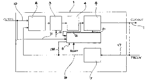
In the block diagram of Fig. 1, the reference 1 denotes as a whole a PLL that,
according to a configuration known per se, comprises the following elements or
modules:
a phase/frequency comparator 2 having associated, as an output circuit, a
circuit 3
of the type commonly called "current pump",
- a loop filter 4 that receives the output signal of the current pump 3,
- an oscillator 5, configured as a VCO (voltage-controlled oscillator) and
driven by the
output signal of the loop filter 4,
- a frequency divider 7, possibly inserted into the feedback loop of the
circuit for the
synthesis function (if required), and
- a general control module 8, destined to allow the reconfiguration of the
circuit
according to the modalities better described hereafter.
As to the divider 7, it must be recalled that the same may operate with both a
CA 02292042 1999-12-10
4
division factor greater than 1 and - in a few applications - a division factor
smaller than
1, thus acting in practice as a multiplier.
The references 20, 21 and 22 show on the whole the lines through which the
control module 8 interacts, according to modalities better described in the
sequel, with
the oscillator 5, the filter 4 and the circuit 3.
Reference CLKIN indicates the signal for which the phase lock and/or the
frequency lock and multiplication functions must be carried out according to
the
exemplary embodiment described herein.
Hereinafter, the signal CLKIN has been assumed to be essentially a clock
signal
with a given frequency. The solution according to the invention is
nevertheless suitable
for application also in situations in which the input signal of the block 2 is
a data signal
for which a clock recovery function is desired. In such a case the "given
frequency"
that is mentioned in the claims attached hereto obviously is the bit rate of
the above
cited data signal. In such event, line 11 will convey in any case a clock
signal, such as
CLKIN.
The signal CLKIN is led over a line 10 to the input of the comparator 2 and,
over
a line 11, to one of the inputs of the control module 8. The latter also
receives, over the
line 21, a signal corresponding to the output of the comparator 2, in
particular the
output signal from the loop filter 4. This choice must however not be
considered as
mandatory: a substantially similar function might be driven, for example,
starting from
the output of the current pump 3. In any case, the driving starting from the
output of
the loop filter 4 proves advantageous since it benefits from the filtering
action
performed by filter 4 itself.
The output signal CLKOUT of the oscillator 5 constitutes the output signal of
the
circuit and is present on a line 14. The same signal can also be sent to a
divider (not
shown here for simplicity) which derives therefrom a frequency-divided output
signal.
A feedback signal FBCLK, present on a line 17, is fed back towards the
comparator 2 through the divider 7 and a line 19. As is easily understood by
the person
skilled in the art, the accessibility of the line 17 from outside the circuit
1 is destined to
allow a greater flexibility in closing the feedback loop. The feedback action
towards
comparator 2 can therefore be effected both starting from the output signal
CLKOUT
present on the line 14 as well as from any other element located downstream of
the
line 14, for instance starting from the frequency-divided output signal. In
the remainder
of the present description it may be however imagined that the feedback line
17 is
directly connected to the output line 14, as schematically shown in the Fig. 1
with a
dashed line.
A preferred characteristic of the circuit 1 (characteristic that is not shown
for
CA 02292042 1999-12-10
simplicity in the general diagram of Fig. 1, but that can in any case be
deduced, for
instance, from Figs. 2 and 3 relating to the structure of individual
components) is the
use of a differential structure, at least for the current pump 3, the loop
filter 4 and the
oscillator 5. The term differential (or balanced) structure indicates in
general a
5 structure wherein the signal transferred from one element to the other is
actually
formed by the difference of the signal value (typically a voltage value)
present on two
complementary lines, respectively positive or negative (or inverting).
This choice offers among other things the advantage of achieving a lesser
sensitivity to noise, in particular to the noise on power supply, giving also
rise to a
lesser generation of disturbances (it is in fact possible to work with smaller
and
complementary signals with circuits that operate in a linear region).
The diagram in Fig. 2 shows in greater detail the structure of the oscillator
5,
implemented according to the typical configuration of the ring oscillator. The
structure,
which is known per se, comprises in the exemplary embodiment shown four delay
elements or stages 23, connected in cascade. The drawing clearly shows the
complementary structure of the respective connecting lines 24 as well as of
the
feedback line 25 which connects (in an inverting manner, i.e. by creating a
negative
feedback) the output of the last delay element 23 with the input of the first
element.
The reference 26 indicates an output buffer which acts on the output signals
of
the element 23 farthest downstream, thereby making them suitable for being
sent over
the line 14.
The reference 27 indicates a control circuit that receives at its input
(preferably in
a complementary configuration, on two lines denoted by 41 and 42 respectively)
the
output signal of the loop filter 4. The circuit 27 further receives, as
configuration control
signals, the signals incoming on the line 20. The oscillator diagram shown in
Fig. 2
provides for the frequency control to be effected by varying the output
impedance of
the individual stage (or element) 23, also aiming at obtaining a constant
voltage range
at the output of the individual stage.
The control module 8 acts on the module 27 in such a way that the VCO
operates according to one among several frequency/voltage characteristics, as
schematically shown in the diagram of Fig. 5.
This Figure depicts the possible behaviours of the frequency/voltage
characteristic of the oscillator 5.
In particular, in an exemplary embodiment tested in a fully satisfactory way,
256
characteristics were present (i.e. 2" with n=8, but the number of the
characteristics
may ideally be any number, thus also different from a power of two). Each
characteristic corresponds to a different driving configuration of the
oscillator 5 by the
CA 02292042 1999-12-10
6
circuit 27, i.e. to a given number of different behaviours of the output
frequency versus
the control signal received from module 8. The availability of such a wide
family of
characteristics allows covering a very wide range of possible variations of
the operating
frequency of the oscillator while keeping low the oscillator gain. The latter
parameter
determines the frequency range of the individual characteristic. The coverage
of a wide
range of operating frequencies is instead achieved just by virtue of the large
number of
available characteristics.
For the sake of clarity, it must be noted that in Fig. 5 only a part of the
above
characteristics has been shown: their density is in fact so high as to make
impossible
the complete reproduction in the scale of Fig. 5.
The behaviour of the characteristics represented is not constant and may be
affected by different factors, such as ambient temperature, possible
variations of the
power supply voltage or different results of the technological process of
fabrication of
the circuit as an integrated circuit. For instance, the person skilled in the
art often
distinguishes between "fast" process parameters and "slov~' process
parameters, since
the variability of the technological process results in practice in a higher
or lower
operating speed of the component.
The above variability factors affect the requirement of making the circuit
according to the invention operate in a wide tuning range (see by way of
example the
range indicated in the introductory part of this description).
The provision of an oscillator 5 arranged to operate according to a
frequency/voltage characteristic selectively identified in a very dense family
of available
characteristics (256 for the exemplary embodiment shown here) allows
optimising the
operation of circuit by adapting the behaviour of the oscillator 5 to the
specific
operating conditions. In particular, the fact that the characteristics of the
family
depicted in Fig. 5 have in their intermediate region an angular coefficient
which
increases when moving upwards along the family, allows implementing an
adaptation
function whose practical consequence is that of keeping limited and
substantially
constant the sensitivity of oscillator 5 (in terms of gain/actual operating
frequency ratio)
as the parameters vary, in particular with an adjustment action that has the
characteristics of an automatic adaptation function.
EP-A 0 915568 describes the possible implementation of an automatic tracking
of the optimum characteristic followed by a permanence on such a
characteristic, in
such a way as to prevent or at least to render very unlikely (unless the
operating
conditions of the device substantially change) subsequent changes of
characteristic. In
the exemplary embodiment described in the previous application the tracking of
the
optimum characteristic is performed starting from an initial point (usually
corresponding
CA 02292042 1999-12-10
7
to the circuit activation) positioned below the diagram of the characteristics
(for this
purpose reference may be made to the diagram of Fig. 5 of the present
application)
and then proceeding to the attainment of the optimum operating point through
subsequent steps or jumps between adjacent characteristics. This solution is
S satisfactory as long as the number of the characteristics potentially to be
examined is
kept low (for example, up to 8 characteristics). When the number of the
characteristics
increases (reaching, for instance, 256, as in the example described here), the
search
for the optimum working point through subsequent jumps between adjacent
characteristics may be penalising in terms of rapidity in attaining the
optimum
operating conditions of the device.
For this reason in the solution according to the invention it is envisaged
that the
achievement of the optimum operating conditions may occur in two subsequent
stages
or phases.
The first phase may be essentially seen as a coarse identification of the
working
point, performed by making the device converge towards one of the two
characteristics
that are the closest ones to the optimum operating point. It will be however
appreciated
that the notation "coarse" given to this phase is not wholly adequate since
such a
phase may result already in the rapid achievement of the optimum operating
condition.
Even if this does not occur, the non-optimum character of the convergence
condition
attained is in all cases marginal, since the achievement of the optimum
condition only
requires in practice the execution of a step corresponding to tha move to an
adjacent,
very close characteristic (just because of the high density of the family of
the allowable
operating characteristics: see in this regard Fig. 5).
We will now examine the structure of control module 8, as shown in Fig. 3,
where
references 30 and 40 are two control units that, by interacting with an
additional pre
bias unit 50, allow implementing the adaptation of the operating
characteristics of the
circuit by performing one after the other the two phases of coarse adjustment
(unit 30)
and fine adjustment (unit 40), previously described.
The unit 30 is essentially a counter that receives the signal CLKIN (through
line
11 ) as well as the output signal of the oscillator 5 or the divider 7, if any
(line 190 of
Fig. 1). So the unit 30 will operate on the frequency given by the input
signal CLKIN
and on a second frequency, which is related in any case to the output
frequency of the
oscillator 5, since it is either the actual output frequency of the oscillator
5 or a sub
multiple or a multiple thereof, if the divider 7 is present. The counter 30
further has a
reset input (at which it receives a signal RESET, see the time diagram of Fig.
6a), and
a further input line 31 which conveys the signal PREPOL coming from the unit
50. That
signal, the behaviour of which is represented in the time diagram of Fig. 6d,
actually
CA 02292042 1999-12-10
g
represents an enabling signal for the unit 30.
The counter 30 has then two output lines 301 and 302, that transfer towards
unit
50 two signals FHIGH and STROBECOARSE, respectively. The first signal
identifies,
as will be better seen in the sequel, the direction of movement in the
exploration by
bands of the family of characteristics of Fig. 5. The second signal
essentially is a
validation signal for the first one.
The unit 40, which is comparable to a certain extent to the whole of the
modules
80 and 81 in EP-A 0 915 568, receives at its input the output signal of the
filter 4
through lines 210 and 211 (forming in the whole line 21 of Fig. 1 ). The unit
40 also
receives the signal PREPOL present on the line 31, in addition to the signal
CLKIN
available on the line 11 and to the reset signal RESET.
The output of the unit 40 consists of two additional lines 401 and 402
conveying
respective signals UP/DOWN and STROBEFINE to unit 50. The first signal
provides
the indication relating to the possible displacement towards the immediately
upper
(UP) or immediately lower (DOWN) characteristic. Also in this case, the second
signal
represents the validation signal for the first one.
The unit 50 receives the signals arriving over the lines 301, 302, 401, 402,
and
the reset signal RESET, and generates at its output:
- on the line 20, the control signal towards the oscillator 5,
- on the line 22, a signal LOCKF1LTER, sent to the circuit 3 and destined to
inhibit the
control action of the loop filter 4 on the frequency of the oscillator 5
during the
phase of search or exploration by bands of the family of characteristics of
Fig. 5,
and
- on the line 31, the signal PREPOL.
The diagram of Fig. 4 shows in even greater detail the generation of the
signals
FHIGH and STROBECOARSE, present on lines 301 and 302, within the unit 30. In
particular, in the diagram of Fig. 4, the reference 310 denotes a circuit
which
implements a time base as a function of the frequency of the signal CLKIN
arriving
over the line 11. The reference 311 denotes a counter such as, for example, a
binary
counter, arranged to count up to a value (for instance equal to 256) depending
on the
accuracy desired for the comparison between the incoming frequencies on the
lines 11
and 190. The counter 311 receives at its input the signal present on the line
190 (in
practice the frequency of the oscillator 5, divided by the division factor of
the divider 7,
if any).
The connection between the time base 310 and the counter 311 is performed
through two lines 3101 and 3102. The line 3101 carries a periodic enabling
signal,
whose duration is determined by the accuracy required for the comparison
between
CA 02292042 1999-12-10
9
the two input frequencies of the unit 30. For instance, such duratibn may be
chosen
equal to 256 times the period of the signal CLKIN present on the line 11. The
line 3102
carries a signal that periodically resets the counter 311 at the end of the
enabling
window corresponding to the signal present on the line 3101. The signal
present on the
line 3102 corresponds in practice to the signal STROBECOARSE. The signal FHIGH
corresponds instead to the overflow output of the counter 311, which output is
caused
to pass through a buffer circuit 312, usually formed by a flip-flop.
With reference to Fig. 6, the four time diagrams denoted by a, b, c, and d
show
the behaviour of the signals RESET, STROBECOARSE, LOCKFILTER and PREPOL,
illustrated respectively:
- in the initial phase of "coarse" identification of the operating
characteristic (pre-bias
phase denoted by A), and
- in the subsequent phase of regular operation, with the enabling of the fine
adjustment function, according to the terms better described in the sequel
(phase
B).
Basically, upon activation, the circuit aims at choosing the best
characteristic (the
one whose rest position is the closest one to the nominal frequency -
determined in
practice by the frequency of the signal CLKIN) through a dichotomic mechanism.
In practice the mechanism of choice of the best characteristic is effected by
exploring the family of the characteristics shown in Fig. 5 by bands of
progressively
narrower width. This occurs in particular on the basis of the following
criteria, described
with reference to the possible presence of 256 characteristics.
Preferably, at the start of the Phase A, the unit 50 acts on the filter 4
through the
signal LOCKFILTER so as to inhibit the frequency control of the oscillator 5
by the filter
4 itself. The unit 50 selects the central characteristic in the family of 256
characteristics, in this case the 128th characteristic.
The reference frequency CLKIN is then compared with the frequency present on
the line 190 and, depending of the outcome of said comparison, i.e. on the
sign of the
difference between such frequencies, there is considered the central frequency
of one
of the two bands into which the family of the operating characteristics
represented in
Fig. 5 is subdivided by the characteristic that has been selected at that
moment (the
128th characteristic in the example).
In practice, if the frequency of the oscillator 5 (divided by divider 7, if
any) is
greater than the reference frequency (positive sign difference), the central
characteristic of the lower band is then considered, and the 64th
characteristic is
chosen. If instead the frequency of the oscillator 5 is lower than the
reference
frequency (negative sign difference), then the central characteristic of the
upper band,
CA 02292042 1999-12-10
i.e. the 192nd characteristic is taken into account.
At this point the operation is repeated within the band previously chosen. The
respective central characteristic - the 192nd or the 64th characteristic -
splits the
respective band into two sub-bands of which the width is half that considered
in the
5 previous choice step. The new frequency of the oscillator 5 is then compared
with the
reference frequency and depending on the comparison outcome, the circuit
passes to
the central characteristic of one of the new bands, hence the characteristic
which is
spaced apart by 32 positions upwards or downwards of the one previously
chosen.
The above operation is repeated for n steps (in this case, eight) until the
circuit
10 settles on the characteristic whose rest frequency is the closest one to
the reference
frequency.
It shall be appreciated that the above procedure of search for the operating
characteristic has a rapid convergence, since the number of steps is related
to the
logarithm with base 2 of the number of characteristics.
An embodiment of the method described on the basis of the circuit structure of
Figs. 3 and 4 may be illustrated referring to the time diagrams of Fig. 6.
On the activation or reset of the circuit (RESET signal applied to the units
30, 40
and 50), the signals LOCKFILTER and PREPOL (Figs. 6c and 6d) become high.
The frequency comparator (blocks 310 and 311 ) is active and the
characteristic
selected by the pre-bias circuit 50 is the central one (the 128th in the
exemplary
embodiment). The action of the control signal coming from the filter 4 is
inhibited (by
signal LOCKFILTER on the line 22) so that the centre of the characteristics is
considered. The frequency comparator start the comparison between the outside
reference frequency CLKIN, present on the line 11, and the frequency of the
oscillator
5 (divided by the divider 7, if any), detected on the tine 190.
In practice, at the end of the enabling interval generated on the line 3101 of
the
block 310, it is checked whether the counter 311 has reached the overflow
condition,
which event indicates that the frequency present on the line 190 is higher
than the
frequency CLKIN present on the line 11. Said event is stored by the flip-flop
312 that
originates the signal FHIGH. Said signal is therefore high if the oscillator
has a
frequency higher than the reference frequency CLKIN, or low if the oscillator
has a
frequency lower than the reference. This information is sent to the pre-bias
circuit 50
by means of a pulse of the signal STROBECOARSE. The unit 50 recognises the
outcome of the comparison effected in the unit 30 and starts the subsequent
comparison phase in such a way that the new frequency corresponding to the
subsequent characteristic to be considered, according to the dichotomic or two-
section
diagram previously seen arrives on the line 190.
CA 02292042 1999-12-10
11
The above operation of comparison and modification of the characteristic used
for the comparison is carried out through the n steps previously described.
Once attained the convergence on the characteristic whose rest frequency is
less far (in frequency) from the reference, the pre-bias circuit 50 recognises
the end of
the phase of coarse search (phase A in Fig. 6), and informs the filter 4, by
means of
the signal LOCKFILTER (Fig. 6c) on the line 22, that it is now possible to
unlock the
control voltage, thus leaving the device free to evolve to the phase locked
function so
as to achieve the phase locked condition to the outside reference.
Preferably, the pre-bias circuit 50 additionally inhibits the frequency
comparator
30 (through the signal PREPOL) for the purpose of minimising power
consumption.
At this point, the unit 30 becomes in practice inactive, whilst the unit 50
operates
under the control of the unit 40, in particular according to the signals
UP/DOWN and
STROBEFINE emitted by unit 40 on the lines 401 and 402.
In practice, the unit 50 acts under the control of the signal STROBEFINE
depending on the value of the UP/DOWN signal: the upwards (UP) and the
downwards
direction (DOWN) are here meant as corresponding to the order according to
which
the characteristics are shown in the diagram of Fig. 5. The UP value
intervenes on the
unit 50 so that the oscillator 5 is made to operate on a higher characteristic
than the
one on which the same oscillator is positioned at that moment. The DOWN value
causes an intervention in the opposite direction.
The signal UP/DOWN is generated by the unit 40 which, from this standpoint,
may be substantially regarded as a double comparator with hysteresis that,
upon
realising the need of effecting a change of characteristic, sends, in addition
to the
signal UP/DOWN, also the relating validation signal STROBEFINE. In this phase
the
unit 50 acts as a finite state machine which intervenes on the oscillator 5,
modifying
the characteristic in the indicated direction of the signal UP/DOWN, when the
module
itself is validated by STROBEFINE.
As an example (for a more complete explanation of these operating modes,
reference can be made to the above mentioned EP-A 0 915 568) it might be
assumed
that the operating point attained at the end of the phase of coarse
convergence is such
that it causes the oscillator to operate at a frequency lower than the desired
one.
The general feedback function of the circuit causes then an increase in the
voltage at the input of oscillator 5. The unit 40 emits the signal STROBEFINE
while the
signal UP/DOWN is high, and the unit 50 starts selecting the immediately
higher
characteristic. Under such conditions, the operating frequency of the
oscillator 5
switches to the value corresponding to the higher characteristic.
The circuit starts then tracking the desired frequency, and moves down
CA 02292042 1999-12-10
12
backwards along the new characteristic attained, entering again at this point
the band
of the comparator with hysteresis (i.e. with the control voltage within the
pre-set limits)
and stabilising at the desired final operating frequency.
The same mechanism of fine adjustment can intervene during the operation to
take into account possible variations in the operating conditions. For
example, under
the hypothesis that the optimum characteristic has been reached in the initial
phase, it
may happen that in steady state operating conditions the device temperature
increases
and such increase causes a downwards shift of all operating characteristics of
the
oscillator. In such a case the circuit detects this event (i.e. the circuit
detects that the
control voltage approaches the end of the range) and causes the switching
(upwards,
in this case) by one characteristic. After waiting for the circuit reaching
again its steady
state operating conditions, a check is made on whether the switching has been
sufficient to restore the system to its correct operating conditions; in the
negative a
new switching is effected. This happens until the operating point of the
device reaches
a position very close to the centre of the characteristic.
Of course, when the change in the operating conditions is substantial, for
instance for the need of making the circuit operate at a new frequency, it is
preferable
to reset the circuit and to activate again the convergence process towards the
desired
operating condition through the phase of "coarse" convergence, previously
illustrated.
Obviously, while the principle of the invention remains unchanged, the
construction details and the embodiments may be widely varied with respect to
what is
described and illustrated herein, without thereby departing from the scope of
the
present invention, as defined in the claims attached hereto.