Note: Descriptions are shown in the official language in which they were submitted.
CA 02292129 2000-06-02
MIJLTI-LAYERED PATCH ANTENNA
Techaical Field
This znvencion relates to microscr~p patch
antennas and to arrays of s~.~.ch antennas and, more
particularly, to a barn fed array for the generation
5 of shaped or pencil beams.
8aclcground Art
In satellite appl~cat_~ons, lens aaLenn.as
are utilixed to form shaped or pencil beams.
Typically, an array of unit ce7_ls are formed on a
10 single lens eomprz.s~ng a dielectric substrate with
one or mare conducting layers. The uriit cells Have
szripline feed members wh~.ch channel electromagnetic
waves_ The stripline feed members vary in length in
order to provide appropriate phase differences
15 required to generate the shaped/pencil beam. The
electromagnetic radiation co be received or
transmitted is typically provided directly co the
Eeed member i.n the form o~ ele:ctrieal power. The
phase versus frequency characteristic of each unit
2a cell is preferably linear in order to maintain the
desired beam shape over a range c~f frequencies.
A problem arises, however, in feeding the
stripline feed members w~.th electromagnetic
radiat~.on. Known devices use direct electrical
25 co.nxZecc~ons between a radiating source and Lrie feed
members to permit ~ransmiss~on_ As an example, a
CA 02292129 1999-12-13
2
typical bootlace lens requires direct electrical
connections between a feeding patch layer, the feed
members, and a transmitting patch layer. Such
connections, or probes, are difficult and expensive
5 to manufacture. Furthermore, these probes produce
temperature stability concerns. Accordingly, there
exists a need for a simplified lens structure capable
of transmitting and receiving shaped or pencil beams,
which has simplified construction.
i o Summary Of The Invention
The present invention discloses a novel
horn-fed, multi-layered, patch antenna which is
capable of transmitting and receiving shaped or
pencil beams without the need for direct electrical
15 connections. The inventive antenna includes an array
of unit cells. Each unit cell includes a
transmitting patch, located on a first patch plane,
and a feeding patch located on a second patch plane.
Interposed between these patches are two ground
20 planes each containing corresponding slots. The
ground planes are separated by feed members which
further correspond with the slots of both ground
planes. These components are all configured within a
dielectric substrate.
25 In operation, the horn emits
electromagnetic waves which strike the second patch
plane. The energy is coupled between the second and
first patch planes via the slots and feed members.
CA 02292129 1999-12-13
3
The feed members vary in length, or size, in order to
provide appropriate phase differences required to
generate the desired shaped or pencil beams. Since
the feed members propagate in the transverse
5 electromagnetic (TEM) mode, the phase versus
frequency characteristic of each unit cell (patch-
slot-feed-member-slot-patch) is linear. This has the
advantage of maintaining the beam shape over a range
of frequencies.
10 The ability of the present invention to
couple energy from the second patch plane to the
first, via slots and feed members, eliminates the
drawbacks of the previous art. Specifically, direct
connections are no longer necessary to couple the
15 feed patches to the transmitting patches or the feed
members. The present invention thus has the further
advantage of eliminating the need for layer piercing
probes thereby simplifying the antenna manufacture.
In addition, the elimination of the probe connection
20 enhances temperature stability.
Other advantages of the inventive antenna
over prior art is its flat structure, and light
weight, making it ideal for packaging within a
satellite application. The linear phase versus
25 frequency characteristics make wide band applications
possible and the antenna's center-fed structure helps
to eliminate dispersion problems.
Additional advantages and features of the
present invention will be apparent from the following
CA 02292129 2000-06-02
4
detailed description when taken in view of the attached drawings and the
claims
appended hereto.
Therefore, in accordance with an aspect of the present invention, there is
provided an antenna structure comprising:
a plurality of unit cells each having:
a first patch plane having a first patch;
a first ground plane adjacent to said first patch plane, said first ground
plane
having a top slot in operative communication with said first patch;
a feed member plane adjacent to said first ground plane, said feed member
plane having a feed member in operative communication with said top slot;
a second ground plane adjacent to said feed member plane, said second ground
plane having a bottom slot in operative communication with said feed member;
a second patch plane adjacent to said second ground plane, said second patch
plane having a second patch in operative communication with said bottom slot;
a first dielectric layer interposed between said first patch plane and said
first
ground plane;
a second dielectric layer interposed between said first ground plane and said
feed member plane;
a third dielectric layer interposed between said feed member plane and said
second ground plane; and
a fourth dielectric layer interposed between said second ground plane and said
second patch plane.
BRIEF DESCRIPTION OF THE DRAWINGS
For a more complete understanding of the invention, reference should now be
had to the embodiments illustrated in greater detail in the accompanying
description
and drawings, in which:
Figure 1 is a lens antenna structure within a satellite environment;
Figure 2 is an exploded perspective view of a partial lens antenna structure
in
accordance with an embodiment of the present invention;
Figure 3 is a top view of a lens antenna structure in accordance with an
embodiment of the present invention;
CA 02292129 2000-06-02
4a
Figure 4 is an embodiment of a unit cell;
Figure S is a partial cross-sectional view of the unit cell of Figure 4 taken
along line 4-4;
Figure 6 is a graph of return loss versus frequency of three different unit
cells
in accordance with an embodiment of the present invention;
Figure 7 is a graph of phase versus frequency of three unit cells in
accordance
with an embodiment of the present invention;
Figure 8 is a graph of feed member length versus phase of three unit cells in
accordance with an embodiment of the present invention; and
CA 02292129 1999-12-13
5
FIGURE 9 is another embodiment of a unit
cell.
Best Models) For Carrying Out The Invention
The present invention will be described in
S terms of its operation in a transmit mode. Due to
the principle of reciprocity, the invention works the
same in a reverse order for the receive mode.
Referring to Figure 1, a lens antenna structure 20 is
preferred for use in a satellite 10 application as a
10 result of its low profile and ease in which it can be
configured to specialized geometries. Structure 20 is
a horn-fed, multi-layered, printed circuit lens
antenna particularly suited for shaped or pencil
beams in the Ku and Ka bands.
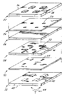
15 Referring to Figure 2, one embodiment of
the lens antenna structure 20 is composed of a series
of stacked layers. A first dielectric layer 22 is
positioned adjacent to a first ground plane 24 which
in turn is positioned adjacent to a second dielectric
20 layer 26. The second dielectric layer 26 is
positioned adjacent to a third dielectric layer 28
which in turn is adjacent to a second ground plane
30. The second ground plane 30 is positioned
adjacent to a fourth dielectric layer 32.
25 Interposed between the second dielectric
layer 26 and the third dielectric layer 28 is a feed
member plane 34. In addition, positioned on a top
CA 02292129 1999-12-13
6
surface 36 of the first dielectric layer 22 is a
first patch plane 38, and positioned on a bottom
surface 40 of the fourth dielectric layer 32 is a
second patch plane 42. In addition, slots 50, 54 are
5 arranged in the first and second ground planes 24, 30
respectively. Feed members 52 corresponding to slots
50, 54 are arranged in the third dielectric layer 28.
In operation, the feed members 52
capacitively and electromagnetically couple the first
10 and second patch planes 38, 42. A horn 44, remotely
positioned below the second patch plane 42, emits
electromagnetic energy in the direction of the
antenna structure. This signal is received by the
second patch plane 42, converted to TEM waves by the
15 slots 50, 54 and feed members 52 in the intermediate
ground planes 24, 30 and dielectric plane 28, and
subsequently transmitted by the first patch plane 38.
Figure 3 is a top view of a lens antenna
structure 20 in accordance with one embodiment of the
20 present invention. As shown in Figure 3, the lens
antenna structure 20 comprises a plurality of unit
cells 46. A unit cell 46 is shown in further detail
in Figure 4.
As shown in Figure 4, each unit cell 46
25 contains a portion of the layers and planes mentioned
above. Each unit cell 46 comprises a first patch 48
from the first patch plane 38, a top slot 50 from the
first ground plane 24, a feed member 52 from the feed
member plane 34, a bottom slot 54 from the second
CA 02292129 1999-12-13
7
ground plane 30, and a second patch 56 from the
second patch plane 42. Each of the elements
comprising the unit cell 46 are separated by a
dielectric substrate.
5 As shown in Figure 5, patch 48 is separated
from slot 50 by the first dielectric layer 22; slot
50 is separated from feed member 52 by the second
dielectric layer 26; feed member 52 is separated from
slot 54 by the third dielectric layer 28; and slot 54
10 is separated from the second patch 56 by the fourth
dielectric layer 32.
Referring again to Figure 4, the first
patch 48 is substantially centered over the top slot
50, and the second patch 56 is centered beneath the
15 bottom slot 54. The first patch 48 is off-centered
from the second patch 56. The feed member 52 has a
first end 58 positioned substantially perpendicular
to the top slot 50, and a second end 60 positioned
substantially perpendicular to the bottom slot 54.
20 The feed member ends 58 and 60 extend to, and
slightly beyond, the slots 50 and 54, respectively.
In operation, the second patch 56 receives
electromagnetic energy from the horn 44. Patch 56
radiates a frequency band centered at the second
25 patch 56 resonance frequency. This radiation induces
an electric field in the bottom slot 54 which extends
transversely to the long dimension of the slot 54.
This electric field creates a TEM wave which travels
along feed member 52. This wave induces a second
CA 02292129 1999-12-13
8
electric field in the top slot 50 which, in turn,
excites first patch 48 at its resonating frequency.
First patch 48 then transmits a frequency band
centered about its resonating frequency.
5 The feed member 52 can be configured in
different shapes. For example, the feed member 52
may be straight, so that the associated top slot 50
is parallel with the associated bottom slot 54, or
the feed member 52 may be bent as shown in Figure 9.
10 The preferred shape of the feed member 52 is a shape
which positions the first end 58 orthogonal to the
second end 60. Such a feed member shape permits
variations of feed member lengths from one unit cell
46 to the next within the same array in a spacially
15 efficient fashion. In addition, the orthogonal
positioning of the first end 58 to the second end 60
simplifies manufacturing and reduces associated costs
since the same patch plane pattern may be utilized
for both the first patch plane 38 and the second
20 patch plane 42. Likewise, the same ground plane
pattern may be utilized for the first and second
ground planes 24, 30.
Referring to Figure 6, "1" represents the
distance from "s" to "s"' along the feed member 52.
25 The slot and patch dimensions are designed to provide
good return loss. For example, with first and second
patch dimensions of 0.5 cm x 0.5 cm, unit cell size
of 0.88 cm x 0.88 cm, top and bottom slot size of 0.4
cm x 0.05 cm, first and fourth dielectric layer
CA 02292129 1999-12-13
9
thicknesses of 0.1 cm with dielectric constant of
1.1, and second and third dielectric layer
thicknesses of 0.038 cm with a dielectric constant of
2.53, the -lSdB return loss bandwidth is
5 approximately 10%. This is true whether 1 - 0.6 cm
as shown in line 100, or 1 - 1.0 cm as shown in line
102, or 1 - 1.4 cm as shown in line 104.
As shown in Figure 7, the feed member 52
propagates in the TEM mode, therefore the phase
10 versus frequency characteristic of the unit cell 46
is linear (lines 106, 107, 108). Thus, the beam shape
can be maintained over a range of frequencies.
The transmitted bandwidth can be increased
by using thicker substrate for the first and fourth
15 dielectric layers 22, 32 and/or using stacked first
patches 48. Preferably, the stacked patches are
approximately equal in size so as to resonate at
approximately the same frequencies, but differ enough
so as to broaden the bandwidth. The dielectric
20 substrate utilized between stacked patches will also
cause broadening of the transmitted frequency
bandwidth. The dielectric constant is higher for the
second and third dielectric layers 26, 28 than for
the first and fourth dielectric layers 22, 32 in
25 order to provide a sufficient electromagnetic
coupling between the first patch 48 and the second
patch 56. Also, for a given off-set between the
patch 48 and patch 56, a high dielectric substrate in
CA 02292129 1999-12-13
10
the feed region provides a large dynamic range for
the phase.
In order to generate shaped or pencil
beams, the lens antenna structure 20 must operate at
5 appropriate phase differences. Phase differences are
provided by varying the length of the feed member 52
from one unit cell 46 to the next. Figure 8
illustrates the phase shift versus feed member 52
length for a representative frequency (line 110).
10 Figure 9 shows another embodiment of a unit
cell. A dual polarization application can be
configured when utilizing a dual unit cell 62. Dual
unit cell 62 is similar to unit cell 46 with an
additional feed member 52 coupled with additional top
15 and bottom slots 50, 54. The additional slots are
spaced apart from, and positioned perpendicular to,
the original slots. This positioning provides the
preferred orthogonal coupling of electromagnetic
radiation for dual polarization applications. The
20 two polarizations are further isolated by a plurality
of holes 64 plated with conductive metallic material
connecting the respective ground planes in which
slots 50 and 54 reside . To ensure proper isolation,
the separation between the plurality of holes 64 is
25 preferably less than 0.2 times the wavelength of the
resonating frequency of the first and second patches
48 and 56.
It should be understood that the inventions
herein disclosed are preferred embodiments, however,
CA 02292129 1999-12-13
11
many others are possible. It is not intended herein
to mention all of the possible equivalent forms or
ramifications of the invention. It is understood
that the terms used herein are merely descriptive
5 rather than limiting, and that various changes may be
made without departing from the spirit or scope of
the invention as defined by the appended claims.