Note: Descriptions are shown in the official language in which they were submitted.
CA 02292222 1999-12-15
TITLE OF THE INVENTION
TIME SWITCH
BACKGROUND OF THE INVENTION
1. Field of the Invention
This invention relates to a time switch for controlling a load
at a predetermined time.
2. Description of the Related Art
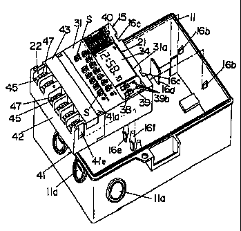
Fig. 18 illustrates an example of this kind of time switch as
related art. This time switch includes a boxed-shaped main casing
11 having a front opened end, a printed circuit board 32' placed in
the main casing 11, and an inner cover plate 12 covering the front
opened end of the main casing 11.
The printed circuit board 32' is equipped with a clock
function block 21 having a liquid crystal display and a plurality
of push buttons, a terminal block 22 for connecting loads, and a
load controlling relay 23. The circuit board 32' is fitted in and
fixed to the main casing 11 by tightening screws 13. The main
casing 11 is coved by an outer cover (not shown). The inner cover
plate 12 is disposed at the front opened end so as to cover the
whole area of the printed circuit board 32' and fixed to the main
1
CA 02292222 1999-12-15
casing 11 by tightening screws 14. In this state, the clock
function block 21 is exposed through the opening 12a formed in the
inner cover plate 12.
However, according to the aforementioned structure, when loads
are connected the terminal block 22, since the inner cover plate 12
covers not only the circuit board 32' but also the terminal block
22, the inner cover plate 12 should be detached from the main
casing 11. As a result, the whole area of the circuit board 32'
(i.e. the parts provided on the circuit boards 32') will be
exposed. This allows a wire of the load and/or a tool such as a
screwdriver to contact the parts, resulting in unintentional
damages to the parts. Furthermore, since the circuit board 32' is
exposed during the connecting operation of the load, foreign
substances may adhere to the parts circuit boards 32' and/or the
load. This may also cause a breakage problem thereof. In
addition, the clock function block is complicated in structure,
resulting in an increased manufacturing cost.
US Patent No. 5,329,082 discloses a time switch equipped with
a mechanical clock function block mounted on a plastic plate and a
circuit board having a terminal block. The circuit board is also
connected to the plastic plate so that the terminal block is
exposed. According to this construction, a connecting operation of
the load to the terminal block may be performed without causing any
problems or damages to the clock function block, and an adherence
by foreign substances can be avoided. Thus, unexpected damages of
2
CA 02292222 1999-12-15
the clock function block or accidents may be avoided. However,
since the terminal block is fixed to the plastic plate together
with the clock function block, in a case where different types of
time switches are manufactured, it is required to manufacture
different types of terminal blocks designed for the respective type
of time switch. Thus, the terminal block cannot be used for
different types of time switch, resulting in an increased
manufacturing cost.
Furthermore, in this structure, in a case where a quality
testing is performed to confirm the functions at the stage of
designing the product, it is required to evaluate not only the
clock function block but also the terminal block. Thus, a larger
number of points should be checked as compared to only checking the
clock function block, which causes an increased labor for the
evaluation.
SUMMARY OF THE INVENTION
An object of the present invention is to provide a time switch
which is simple in structure and low in manufacturing cost.
Another object of the present invention is to provide a time
switch in which an connecting operation of a load to a terminal
block can be performed without causing any damages or problems.
Still another object of the present invention is to provide a
time switch which can easily perform an evaluation test.
3
CA 02292222 1999-12-15
Yet another object of the present invention is to provide a
time switch having a common part which can be used for different
types of time switches.
According to a first aspect of the present invention, a time
switch includes a circuit board equipped with a time switch circuit
and a display for displaying a time-schedule set by a user and a
current time, an operation unit having a plurality of push buttons
for setting the time-schedule and the current time, and a casing in
which the circuit board and the operation unit are accommodated,
the casing having a plurality of openings for fitting the plurality
of push buttons. The operation unit includes a resilient sheet
member integrally equipped with the plurality of push buttons and
a plurality of conductive contact members each disposed on a
portion corresponding to each of the plurality of push buttons.
The circuit board has pairs of contact portions. Each pair of the
contact portions is to be electrically connected via the conductive
contact member while the push button is being depressed. The
operation unit is supported by the casing and the circuit board in
a state that a peripheral portion of the sheet member is clamped by
and between an inner surface of the casing 4nd the circuit board
with the plurality of push buttons fitted in the plurality of
openings.
With this time switch, since the operation unit is supported
by the casing and the circuit board, the time switch can be simple
in structure, resulting in an easy assembly and a reduced
4
CA 02292222 1999-12-15
manufacturing cost.
According to a second aspect of the present invention, a time
switch includes a circuit board=equipped with a time switch circuit
and a display for displaying a time-schedule set by a user and a
current time, an operation unit having a plurality of buttons for
setting the time-schedule and the current time, a casing in which
the circuit board and the operation unit are accommodated, the
casing having a plurality of openings for fitting switches and
pilot lamps provided on the circuit board, and a display sheet
attached on a surface of the casing, the display sheet having a
plurality of openings for exposing the switches and pilot lamps.
The number of the openings formed in the casing corresponds to the
maximum number of the switches and pilots lamps to be provided on
the circuit board. Furthermore, the number of the opening formed
in the display sheet corresponds to the number of the switches and
pilots lamps actually provided on the circuit board, whereby some
of the opening formed in the casing not in use are covered by the
display sheet.
With this time switch, even in a case where the operation of
the circuit board and/or the number of parts provided on the
circuit board are changed, it is only required to change a display
sheet to be attached on the casing. In other words, it is not
required to change the casing. As a result, the storage space can
be decreased, and various types of time switches can easily be
provided.
5
CA 02292222 1999-12-15
Other objects and advantages of the present invention will
become apparent from the description of the preferred embodiments,
which may be modified in any manner without departing from the
scope and spirit of the present invention.
BRIEF EXPLANATION OF THE DRAWINGS
Fig. 1 is an explode perspective view of a main portion of a
time switch according to a first embodiment of the present
invention;
Fig. 2 is a perspective view of the main portion in a state
that the main portion is detached from an outer main casing;
Fig. 3 is a perspective view of the main portion in a state
that a terminal holder is detached from the inner main casing;
Fig. 4 is an enlarged cross-sectional view of the inner main
casing;
Fig. 5 is an exploded perspective view of the clock function
block;
Fig. 6A is a top view of the operation unit;
Fig. 6B is a side view of the operation unit;
Fig. 7 is an enlarged cross-sectional view of the operation
unit;
Fig. 8 illustrates a pair of contact portions;
Fig. 9 is a partially enlarged cross-sectional view of the
operation unit,
6
CA 02292222 1999-12-15
Fig. 10 is a perspective view of a terminal holder in a state
that a holder cover is detached from the main terminal holder;
Fig. 11 is an exploded perspective view of the terminal
holder;
Fig. 12 is a perspective view of the reversed side of the
terminal holder;
Fig. 13 is a cross-sectional view of the connecting portion of
the terminal holder and the outer main casing;
Fig. 14 is a perspective view of the outer main casing;
Fig. 15 illustrates a block diagram of the time switch
circuit;
- Fig. 16 is an exploded perspective view of a main portion of
a time switch according to a second embodiment of the present
invention;
Fig. 17 illustrates a block diagram of the time switch circuit
of the second embodiment; and
Fig. 18 is an exploded perspective view of a time switch
according to a related timeswitch.
DETAILED DESCRIPTION OF THE PREFERRED EMBODIMENTS
Preferred embodiments of a time switch according to the
present invention will now be described in detail with reference to
the accompanying drawings.
(First Embodiment)
7
CA 02292222 1999-12-15
As shown in Fig. 2, the time switch includes a front cover
(not shown), an outer main casing 11 and an inner casing 15 mounted
in the outer main casing 11. The outer main casing is covered by
the inner casing 15 is comprised of an inner main casing 31 and a
terminal holder 41 detachably connected to the inner main casing 31
(see Fig. 3). The inner main casing 31 has a clock function block
21 including an electric timer circuit (see Fig. 1) The terminal
holder 41 includes a terminal block 42 to which a power source and
loads are connected and a load controlling relay 23 (see Fig. 10).
As shown in Figs. 1 and 4, the inner main casing 31 is a box-
shaped casing with a lower opened end and a rear opened end, and
covers a printed circuit board 32 equipped with the clock function
block 21. The printed circuit board 32 is fitted in and fixed to
the inner main casing 31 by tightening screws 33 inserted through
the printed circuit board 32 from the rear side thereof. The
printed circuit board 32 is equipped with a liquid crystal display
(hereinafter referred to as "LCD") 34. As shown in Fig. 5, the LCD
34 is electrically connected to the printed electric circuits of
the printed circuit board 32 via a connector plate 34a made of
conductive rubber. Between the LCD 34 and the printed circuit
board 32, a sponge-like cushion sheet 34b is disposed. The LCD 34
is.secured to the printed circuit board 32 by a shallow box-shaped
display casing 34c made of transparent resin. The LCD 34 is
secured to the printed circuit board 32 via the cushion sheet 34b
and the connector plate 34a by fixing the display casing 34c to the
8
CA 02292222 1999-12-15
circuit board 32 in such a state that the LCD 34 and the connector
plate 34a are fitted in the display casing 34c. Thus, the LCD 34
is electrically connected to the printed circuit board 32. The
display casing 34c is secured to the printed circuit board 32 by
engaging the engaging ledges 34d formed at the rear peripheral edge
of the display casing 34c with the corresponding engaging holes 32a
provided in the printed circuit board 32.
The time switch according to this embodiment is provided with
a plurality of operation buttons S for setting the current time and
for setting the time for operating the loads connected to the time
switch. As shown in Figs. 6A and 6B, these operation buttons (push
button) S are integrally formed on a front surface of the sheet
member 35 having rubber elasticity. As shown in Fig. 7, the sheet
member 35 has, at its rear surface, a plurality of tapered dented
portions 35a each formed at a portion corresponding to the
operation buttons S. Each of the tapered dented portions 35a has
a slanted peripheral wall gradually decreasing the diameter from
the rear surface of the sheet member 35 toward the front surface
thereof. The peripheral wall is formed to be thinner than the
other portion of the sheet member 35. At the bottom of each dented
portion 35a, a conductive movable contact member 35b is fixed such
that the lower surface thereof is inwardly located with regard to
the rear surface of the sheet member 35. Accordingly, when the
operation button S is depressed, the peripheral wall of the dented
portion 35a corresponding to the depressed operation button S is
9
CA 02292222 1999-12-15
warped downward to cause the downward movement of the movable
contact member 35b. Thus, the movable contact member 34b protrudes
from the rear surface of the sheet member 35 toward the printed
circuit board 32. From this state, when the depressing force of
the operation button S is released, the movable contact member 35b
returns to its original position due to the elasticity of the sheet
member 35. As shown in Figs. 1 and 8, the printed circuit board 32
has pairs of conductive printed patterns (contact portions) 32b,
each pair being a combination of a generally Y-shaped conductive
printed pattern and an inverted generally Y-shaped conductive
printed pattern. When the operation button S is depressed, the
movable contact member 35b contacts to a corresponding pair of
conductive printed patterns 32b to cause an electrical conduct of
the pair of generally Y-shaped conductive printed patterns 32b.
This functions as a momentary-type press button, i.e., a button
which becomes ON state only when the button is being depressed.
Thus, a so-called rubber switch is formed by the sheet member 35
and the printed circuit board 32.
As shown in Fig. 1, the inner main casing 31 has a display
window 31a for exposing the LCD 34 at the front wall and a
plurality of openings 31b for fitting the operation buttons S. The
sheet member 35 is attached to the inner main casing 31 in a state
that a portion of the sheet member 35 other than the operation
buttons S is pressed against the inner surface of the inner main
casing 31 by the printed circuit board 32. In detail, as shown in
CA 02292222 1999-12-15
Figs. 4 and 9, a plurality of supporting ribs 31c are formed on the
inner surface of the inner main casing 31, and a whole peripheral
edge and longitudinal central portion of the sheet member 35 are
sandwiched between the supporting ribs 31c and the circuit board
32. Each supporting rib 31c surrounds the periphery of the
opening 31b to prevent the peripheral portion of the opening 31b
from being deformed when the operation button S is depressed.
As will be mentioned later, in this embodiment, the time
switch can control two circuit loads individually. In detail, the
time switch can select any one of operation modes among the first
to third operation modes (1) to (3), i.e., the first operation mode
(2) in which loads can be individually turned ON and OFF by the
timer circuit, the second operation mode (2) in which all loads are
kept in an ON-state regardless of the operation of the timer
circuit, and the third operation mode (3) in which all loads are
kept in an OFF-state regardless of the operation of the timer
circuit. The selection of the operation mode is performed by slide
switches SW1 and SW2 equipped on the printed circuit board 32 and
provided for each timer circuit as shown in Fig. 1. The printed
circuit.board 32 has two operation pilot lamps Li and L2 each made
of a light-emitting diode for showing the operation state of each
timer circuit, and one power pilot lamp L3 for showing the power
ON%OFF state.
The clock function block 21 is provided with a battery B such
as a lithium battery as a back-up power source in case of a power
11
CA 02292222 1999-12-15
failure of the commercial power source. The battery B is provided
to a battery board 36 which is a member separated from the printed
circuit board 32. The battery board 36 is a member separated or
detached from the printed circuit board 32. The battery board 36
is held by holding ribs (not shown) each upwardly protruding from
the inner surface of the inner main casing 31. Furthermore, a part
of the battery board 36 is cramped by and between the inner surface
of the inner main casing 31 and the circuit board 32 so as to be
severely fixed to the inner main casing 31. The battery board 36
is electrically connected to the printed circuit board 32 by way of
electric wires 37 having a connector (receptacle) 37a at its one
end. The printed circuit board 32 has a connector (post) 37b for
detachably connecting the connector (receptacle) 37a. Therefore,
in a case where the battery B is disposed or replaced, the battery
board 36 can be detached from the printed circuit board 32 by
disconnecting connectors 37a and 37b. Thus, the battery B can be
disposed easily and safely, which in turn avoids the pollution of
the environment due to the contents of the battery B and enhances
the re-use of the contents of the battery B.
Th.e inner main casing 31 has a dented portion 31d at the right
side of the display window 31a. Provided at the bottom of the
dented portion 31d are openings 31e for fitting the operation pilot
lamps L1 and L2 and the power pilot lamp L3 and openings 31f for
fitting operation handles 38 of switches SW1 and SW2. A display
sheet 39 made of opaque material is disposed in the dented portion
12
CA 02292222 1999-12-15
31d and adhered thereto by gluing or fusing it. In case where two
switches SW1 and SW2 are provided to the time switch as described
above, the display sheet 39 should have two openings 39a for the
operation handles 38 and three openings 39b for the two operation
pilot lamps Ll, L2 and one power pilot lamp L3 so that these pilot
lamps can be visually confirmed. In a case where a single switch
SW1 or SW2 is provided to the time switch, the display sheet 39
should have only one opening 39a for the handle of the switch and
two openings 39b for the pilot lamps L1 (or L2) and L3. As it is
understood from the above, by selecting an appropriate display
sheet 39 having a different number of openings 39a, 39b and
applying it to an inner main casing 31 having a maximum number of
openings 31f and 31e, the inner main casing 31 can be commonly used
for any type of time switches having a different number of the
switches SW1, SW2. The relationship between the display sheet 39
and the inner main casing 31 is not limited to the aforementioned
embodiment. For example, the maximum number of openings for the
switch handles and the pilot lamps may be provided to the inner
main casing 31, and some of the openings which are not in use may
be covered by the display sheet 39 so as not to be visually
confirmed.
On the front surface of the inner main casing 31 at the left
side of the display window 31a, a time conversion table 40 showing
the relationship between the 24-hour scale and the 12-hour scale is
provided. In the time conversion table, the 24-hour scale and the
13
CA 02292222 1999-12-15
12-hour scale are provided side by side so that the user can easily
convert one into the other. The 12-hour scale is accompanied by
the letters, "am" or "pm". For example, if the 24-hour scale is
shown as: 0:00; 3:00; 6:00; 9:00; 12:00; 15:00; 18:00; and 21:00,
the 12-hour scale will be shown as: 0:OOam; 3:00am; 6:00am; 9:00am;
0:OOpm; 3:00pm; 6:00pm; and 9:00pm. This table enables the user
who lives in a country or region where the 12-hour scale is mainly
employed to use the time switch employing the 24-hour scale
display. In other words, the user can easily convert the time
scale displayed on the LCD 34 in the 24-hour scale into the 12-hour
scale. Thus, even if the user is not familiar with the 24-hour
scale, the user can correctly set the time switch by converting the
24-hour scale displayed on the display 34 into the 12-hour scale.
The time conversion table 40 may be printed by a silk printing
method or a tampon printing method. Alternatively, a sheet on
which the time conversion table 40 is printed may be adhered to the
inner main casing 31. In a case where the time conversion table 40
is provided, the description or appearance of the time scale
displayed on the LCD 34 may preferably be the same as in the time
conversion table 40 to enable an easy conversion of the time scale
by utilizing the time comparison table 40.
As already mentioned above, the terminal holder 41 is
connected to the inner main casing 31. As shown in Fig. 3, the
inner main casing 31.has a channel-shaped connection portion 31g
protruding from the lower edge thereof. The connection portion 31g
14
CA 02292222 1999-12-15
is provided with a pair of guide grooves 31h extending in the fore
and aft directions (the up-and-down direction in Fig. 3) at the
basal end of the connection portion 31g. The connection portion
31g is provided with a pair of outwardly protruded flange portions
31i formed at the rear ends thereof and a pair of outwardly
protruded engaging protrusions 31j formed at the side surface of
the connection portion 31g.
On the other hand, as shown in Fig. 12, the terminal holder 41
has a generally C-shaped connection body 41a with a pair of
inwardly protruded guide edges 41b formed at the upper edges of the
side walls (at the right hand end of the side walls in Fig. 8)
Furthermore, the terminal holder 41 has engaging dented portions
41c at the inside surfaces of the side walls for engaging the
fixing protrusions 31j of the inner main casing 31. The connection
body 41a has cut-out portions 41d at the upper rear ends of the
connection body 41a (at the upper right hand ends of the side walls
of the connection body 41a in Fig. 12) for fitting the flange
portions 31i. Therefore, when the terminal holder 41 is slid
rearward with the guide edges 41b and 41b fitted in the guide
grooves. 31h, the engaging protrusions 31j are engaged with the
engaging dented portions 41c, resulting in an integral coupling of
the inner main casing 31 and the terminal holder 41.
As shown in Figs. 10 and 11, the terminal holder 41 includes
a main terminal holder 42 and a holder cover 43 disposed on the
main terminal holder 42. In detail, the main terminal holder 42
CA 02292222 1999-12-15
has, at its upper central portion, a central dented portion 42a
extending in the longitudinal direction thereof. The central
dented portion 42a is covered by the holder cover 43, and is
communicated to an inner space of the connection body 41a. The
holder cover 43 is provided with a pair of rearwardly protruded
engaging ledges 43a at the longitudinal opposite edges thereof.
Thus, the holder cover 43 is connected to the main terminal holder
42 by engaging the engaging ledges 43a with the engaging holes 42b.
At the front lower end portion of the main terminal holder 42, a
plurality of terminal holding dented portions 42d separated by a
plurality of partitions 42c are provided. The holder cover 43 has
a partitioning wall 43b having a plurality of slits 43c, and is
connected to the main terminal holder 42 such that the partitioning
wall 43b is located between the central dented portion 42a and the
terminal holding dented portions 42d so as to partition them with
the partitions 42c fitted in the slits 43c.
In the central dented portion 42a, a circuit board 44 is
mounted. The circuit board 44 is equipped with two relays 23 and
circuit parts driven by a commercial power for driving the relays
23. AS shown in Fig. 11, the circuit board 44 is also equipped
with a connector (post) 44a for electrically connecting the circuit
board 44 to the circuit board 32 mounted to the inner main casing
31. As shown in Fig. 13, the connector 44a is detachably connected
to a connector (receptor) 44c provided at an end of electric wire
44b which is connected to the circuit board 32. The circuit board
16
CA 02292222 1999-12-15
44 is brazed to terminals 45 to which a commercial power source is
supplied. The terminals of the relay 23 are brazed to terminals 45
to which a load is connected. Each terminal 45 is disposed in each
terminal holding dented portion 42d and fixed to the main terminal
holder 42 by engaging a terminal bolt 47 with a nut 46 disposed at
the bottom of the dented portions 42d. Each terminal 45 has fixing
legs 45a protruding rearward at the right and left side edges
thereof as shown in Fig. 11, and fixed to the main terminal holder
42 with the fixing legs 45a inserted into the bottom of the dented
portion 42d.
Since the central dented portion 42a and the terminal holding
dented portions 42d are partitioned by the partitioning wall 43b of
the holder cover 43, electric wires are prevented from contacting
to the circuit board 44 during connecting operation of the electric
wires to the terminals 45. In addition, the circuit board 44 is
prevented from being adhered by foreign substances. In the
meantime, as shown in Figs. 12 and 13, the main terminal holder 42
has penetrated openings 42e at its appropriate portions for an
easier brazing operation for connecting the terminal 45 to the
circuit.board 44 and/or the relay 23.
As is apparent from the structure shown in Fig. 11, since each
component to be mounted to the terminal holder 41 is assembled to
the main terminal holder 42 from its front side, each component can
be attached to the main terminal holder 42 from one direction,
which facilitates the assembling operation. In detail, the nuts 46
17
CA 02292222 1999-12-15
are attached to the main terminal holder 42. Next, each of the
terminals 45 is forcibly fitted into each of the terminal holding
dented portion 42d, and then the terminal bolt 47 is engaged with
the nut 46. Thereafter, the circuit board 44 is inserted into the
central dented portion 42a, and then the relays 23 are attached.
The relay 23 is held by a pair of holding ledges 42f protruded from
the bottom of the central dented portion 42a, as shown in Figs. 10
and 11. At this stage, the main terminal holder 42 is turned over,
and the brazing is carried out through the penetrated opening 42e.
At this time, functions of the parts mounted to the terminal holder
41 are examined. After the examination, the fabrication of the
terminal holder 41 is accomplished by attaching the holder cover 43
on the main terminal holder 42.
As mentioned above, the inner casing 15 is formed by
integrally connecting the inner main casing 31 and the terminal
holder 41, and is accommodated in the outer main casing 11. As
shown in Fig. 14, the outer main casing 11 has, at its inner
surface of the rear wall, a plurality of supporting ribs 16a on
which the inner casing 15 is placed. On the inside surface of the
upper wall (right side wall in Fig. 14) of the outer main casing
11, a pair of engaging protrusions 16b are formed. Thus, the inner
main casing 31 is fixed in the outer main casing 11 by engaging the
engaging protrusions 16b with the corresponding engaging
protrusions (not shown) formed in the sliding grooves 16c. On the
inside surfaces of the right and left side walls of the outer main
18
CA 02292222 1999-12-15
casing 11, a pair of hooks 16d are formed, whereby the engaging
portions of the hooks 16d are engaged with the dented portions 41e
each formed on the side upper portion of the terminal holder 41.
Thus, the terminal holder 41 is fixed to the outer main casing 11.
In other words, the inner casing 15 is fixed to the outer main
casing 11 by the engaging protrusions 16b and the hooks 16d. Since
the inner casing 15 is supported by the front ends (upper ends in
Fig. 14) of the supporting ribs 16b, a space is formed between the
inner surface of the rear wall (bottom wall in Fig. 14) of the
outer main casing 11 and the rear surface of the inner casing 15.
Therefore, a plurality of ribs 16e are formed on the inner surface
of the rear wall (bottom wall in Fig. 14) of the outer main casing
11 so as to seal the gap formed between the inner surface of the
rear wall (bottom wall in Fig. 14) of the outer main casing 11 and
the lower rear edge of the terminal holder 41. These ribs 16e
prevent an invasion of foreign substances into the inner casing 15
through the aforementioned gap although the inner casing 15 has an
opened portion at its rear side. The outer main casing 11 has
bosses 16f at its inner surface of the rear wall so as to be
located at portions corresponding to the terminal bolts 47. Thus,
these bosses 16f contact to the rear surface of the terminal holder
41 to support the force imparted to the terminal holder 41 when the
terminal bolt 47 is being tightened.
As shown in Figs. 2 and 14, the outer main casing 11 has
knockout portions lla each having an easy-broken-thin peripheral
19
CA 02292222 1999-12-15
portion at the lower side walls, the lower end wall and the lower
end portion of the rear wall. By removing the knockout portions
lla, openings for introducing external wires into the outer main
casing 11 can be formed.
In this embodiment, although the inner casing 15 is connected
to the outer main casing 11 by the engaging protrusions 16b and the
hooks 16d, the inner casing 15 may be connected to the outer main
casing 11 by screws, or by bolts and nuts. Furthermore, the inner
main casing 31 may be connected to the terminal holder 41 by screws
or the like. In the first embodiment, although the printed circuit
board 32 is electrically connected to the circuit board 44 via the
connectors 44a and 44c, they may be directly connected each other,
i.e., without using the connectors 44a and 44c. Similarly, the
battery board 36 may be connected to the printed circuit board 32
without using the connectors 37a and 37b.
Fig. 15 illustrates a circuit structure of this embodiment.
Fig. 15 also illustrates the relationship between the inner main
casing 31 and the terminal holder 41 and the arrangement of the
circuits on the circuit boards 32 and 44 which are mounted in the
inner main casing 31 and the terminal holder 41, respectively.
The terminals 45 used as power terminals 51a are connected to
the circuit board 44, and the terminals 45 used as load terminals
51b are connected to the relays 23. In this embodiment, two relays
23 are provided. Each relay 23 is controlled by a driving circuit
52 equipped to the circuit board 44. Electric power supplied from
CA 02292222 1999-12-15
the commercial power source via the power terminals 51a is supplied
to the driving circuits 52 by way of the rectification circuit 53
and the voltage stabilizingcircuit 54. The rectification circuit
53 and the voltage stabilizing circuit 54 are equipped to the
circuit board 44.
The clock function block 21 includes a microcomputer 60
realizing a clock function for clocking the current time and a
timer function for setting the time schedule. The microcomputer 60
clocks the current time based on the clock signals supplied from
the clock oscillator circuit 61, and is operated based on the clock
signals supplied from the system clock oscillator circuit 62. The
rubber switches having the operation buttons S are arranged in a
matrix arrangement to form the key matrix 63. The key matrix 63
recognizes which of the operation buttons S is depressed to obtain
operation information, and then supplies the operation information
to the microcomputer 60.
The microcomputer 60 is controlled by the mode-change input
circuit 64 so as to select one of its operation modes. The
operation modes include an operation mode for independently
controlling two load circuits as in this embodiment, an operation
mode for collectively controlling two load circuits, an operation
mode for controlling loads based on a weekly time schedule, and an
operation mode for controlling loads based on a daily time
schedule. In other words, different kinds of programs are
installed in the microcomputer 60. One of them is selected by the
21
CA 02292222 1999-12-15
mode-change input circuit 64, and is executed by the microcomputer
60. Also connected to the microcomputer 60 are the LCD 34, the
operation pilot lamps L1, L2, and the power pilot lamps L3.
Further connected to the microcomputer 60 is the back-up battery B
for supplying a power to keep both the clock function and the set
time-schedule in case of a power failure or the like.
The printed circuit board 32 is provided with a rectification
circuit 65 connected to the power terminals 51a. The pulsating
voltage outputted form the rectification circuit 65 is stabilized
by the voltage stabilizing circuit 66. The output of the voltage
stabilizing circuit 66 turns on the power pilot lamp L3. The
output of the voltage is supplied to the microcomputer 60 via
another voltage stabilizing circuit 67 as a power source of the
microcomputer 60. The output of the voltage stabilizing circuit 67
is supplied to the power failure detection circuit 68. The power
failure detection circuit 68 detects the power failure of the
commercial power source based on the drop of the output voltage of
the voltage stabilizing circuit 67. When the power failure is
detected by the power failure detection circuit 68, the
microcomputer 60 stops all functions other than the essential
functions, such as a clock function that are required to be kept
working during a power failure. When the commercial power source
is restored, the microcomputer 60 detects the restoration and
resumes all of the functions. Since the back-up battery B supplies
the electric power to the limited functions required to be kept
22
CA 02292222 1999-12-15
alive during the power failure, only very small amount of electric
power is consumed_during the power failure. As a result, if a
lithium battery or the like is used as the back-up battery B, it is
not required to replace it with a new one for ten or more years.
When the time schedule set in the microcomputer 60 is executed
by operating the operation buttons S, the microcomputer 60 supplies
an instruction to the relay driving signal generation circuit 69
when the current time comes to coincide with the set time of the
time schedule. Then, a driving signal is outputted from the relay
driving signal generation circuit 69 driven by the driving circuit
52 to control the relay 23. In this embodiment, since two relay
driving signal generation circuits 69 are provided for individually
controlling the relays 23, two load circuits can be controlled
separately. Thus, each output state of the relays 23 can be
selected by the two switches SW1 and SW2.
(Second Embodiment)
The time switch according to the second embodiment can
control two circuit loads as understood from Fig. 17. However,
these two loads are not separately controlled as in the first
embodirqent, but are controlled in the same manner. In summary, two
relays 23 are connected in series or in parallel, and single relay
driving signal generation circuit 69 and single driving circuit 52
are provided. This circuit structure only requires one operation
pilot lamp Ll and one switch SW1. If an inner main casing 31 for
accommodating the circuit as shown in the first embodiment which
23
CA 02292222 1999-12-15
individually controls two loads and an inner main casing 31 for
accommodating the circuit as shown in the second embodiment which
controls two loads in the same manner are manufactured separately,
the manufacturing costs will increase and a large space for
accommodating such inner main casings 31 will be required because
of the different types of inner main casings 31. Accordingly, in
this embodiment, the same inner main casing 31 is commonly used for
both the aforementioned circuits, and different display sheets 39
are selectively used for the inner main casing 31. In detail, in
this embodiment, as shown in Fig. 16, the display sheet 39 is
provided with a single opening 39a for the handle of the single
switch SW1 and two openings 39b for one operating pilot lamp L1 and
one power pilot lamp L3. Thus, the display sheet 39 covers the
unused openings 31f and 31e formed in the dented portion 31d of the
inner main casing 31 so as not to expose these openings. The other
structures and operations are the same as in the first embodiment.
According to the first aspect of the present invention, a time
switch includes a circuit board equipped with a time switch circuit
and a display for displaying a time-schedule set by a user and a
current time, an operation unit having a plurality of push buttons
for setting the time-schedule and the current time, and a casing in
which the circuit board and the operation unit are accommodated,
the casing having a plurality of openings for fitting the plurality
of push buttons, wherein the operation unit includes a resilient
sheet member integrally equipped with the plurality of push buttons
24
CA 02292222 1999-12-15
and a plurality of conductive contact members each disposed on a
portion corresponding to each of the plurality of push buttons,
wherein the circuit board has a plurality of pairs of contact
portions, each pair of contact portions being to be electrically
connected via the conductive contact member while the push button
is being depressed, and wherein the operation unit is supported by
and between the casing and the circuit board in a state that a
peripheral portion of the sheet member is clamped by and between an
inner surface of the casing and the circuit board with the
plurality of buttons fitted in the plurality of openings.
With this time switch, since the operation unit is supported
by the casing and the circuit board, the time switch can be simple
in structure, resulting in an easy assembly and a reduced
manufacturing cost.
In the aforementioned time switch, the time switch circuit may
have a clock function for clocking the current time and a time-
schedule setting function for setting the time-schedule, and
includes a load controlling circuit for controlling a load
connected to the time switch when the current time comes to
coincide with the set time-schedule.
It is preferable that the casing includes a main casing in
which the circuit board and the operation unit are mounted and a
terminal holder having a terminal block for connecting a commercial
power source and a load, and wherein the main casing is detachably
connected to the terminal holder. According to this structure, a
CA 02292222 1999-12-15
connecting operation of a load to the terminal holder can be safely
performed because the circuit board is not exposed during the
connecting operation of the board. Since the terminal holder can
be detached from the main casing, only the circuit board
accommodated in the main casing can be subjected to the test
operation. Thus, it is not required to evaluate the terminal
block, resulting in a reduced check points. Furthermore, the
terminal holder can be commonly used for different types of time
switch circuits.
According to another aspect of the present invention, a time
switch including a circuit board equipped with a time switch
circuit and a display for displaying a time-schedule set by a user
and a current time, an operation unit having a plurality of buttons
for setting the time-schedule and the current time, a casing in
which the circuit board and the operation unit are accommodated,
the casing having a plurality of openings for fitting switches and
pilot lamps provided on the circuit board, and a display sheet
attached on a surface of the casing, the display sheet having a
plurality of openings for exposing the switches and pilot lamps,
wherein the number of the openings formed in the casing corresponds
to the maximum number of the switches and pilots lamps to be
provided on the circuit board, and wherein the number of the
opening formed in the display sheet corresponds to the number of
the switches and pilots lamps actually provided on the circuit
board, whereby some of the opening formed in the casing not in use
26
CA 02292222 1999-12-15
are covered by the display sheet.
With this time switch, even in a case where the operation of
the circuit board and/or the number of parts provided on the
circuit board are changed, it is only required to change a display
sheet to be attached on the casing. In other words, it is not
required to change the casing. As a result, the storage space can
be decreased, and various types of time switches can easily be
provided.
The time switch circuit may have a clock function for clocking
the current time and a time-schedule setting function for setting
the time-schedule, and includes a load controlling circuit for
controlling a load connected to the time switch when the current
time comes to coincide with the set time-schedule.
It is preferable that the casing includes a main casing in
which the circuit board and the operation unit are mounted and a
terminal holder having a terminal block for connecting a commercial
power source and a load, and wherein the main casing is detachably
connected to the terminal holder. According to this structure,
a connecting operation of a load to the terminal holder can be
safely performed because the circuit board is not exposed during
the connecting operation. Since the terminal holder can be
detached from the main casing, only the circuit board accommodated
in the main casing can be subjected to the test operation. Thus,
it is not required to evaluate the terminal block, resulting in a
reduced check points. Furthermore, the terminal holder can be used
27
CA 02292222 2007-06-06
for any types of time switch circuits.
It is preferable that the time switch further includes a time
conversion table for converting a 12-hour time scale into a 24-hour
scale, and vice versa. With this time switch, an easy conversion
of the time scale can be performed even if the displayed time scale
is not familiar to the user.
It is preferable that the time conversion table is provided on
an outer surface of the casing.
It is also preferable that the time conversion table is
located next to the display, and that the display displays the same
type of character as that used in the time conversion table.
The terms and expressions which have been employed herein are
used as terms of description and not of limitation, and there is no
intent, in the use of suph terms and expressions, of excluding any
equivalents of the features shown and described or portions
thereof, but it should be recognized that various modifications are
possible within the scppe of the invention claimed.
28