Note: Descriptions are shown in the official language in which they were submitted.
CA 02292594 2003-11-21
DIFFRACTIVE SURFACE PATTERN
The invention relates to surface patterns of the kind set forth in the
classifying portions of claims 1 and 2 to the use of that surface pattern.
Such surface patterns are suitable as security and authenticity features on
documents such as for example bank notes, value-bearing papers or securities,
and
bonds, identity papers, passes, credit and other identity cards, smart cards
in any
form and so forth.
Patent specifications EP-A 105,099, EP-A 330,738, EP-A 375,833 and EP
A 537,439 disclose optically diffractive security features which are embossed
in
plastic material, with patterns and extremely fine filigree structures, such
as for
example guilloche patterns, the image content of which changes in a
predetermined
fashion upon being turned about an axis. Those security features do not
involve
machine-readable information.
Such security features are embedded in a plastic laminate (EP-A 401,466)
and can be glued onto a substrate.
Volume holograms are also known (H. J. Caulfield: "Handbook of Optical
Holography", pages 202-204, 228-229, Academic Press, Inc., 1979, ISBN 0-12-
165350-1). Starting from a light sensitive film or foil, the hologram is
produced by
exposure with reference and object beams from a laser, wherein the
interferences
between the reference beam and object beams produce local changes in the
refractive index in the foil, which are present locally in the form of closely
stepped
planes arranged in a Venetian blind-like configuration (_ "fringes") within
the
thick, light sensitive layer. After development the film is practically
transparent
while at the same time under predetermined conditions the light which
penetrates
into the film is diffracted with a high degree of efficiency at the fringes.
From US patent 5,379,131, it is well known to provide an arranged bar
code within a diffraction grating pattern, whose narrow and parallel regions
likewise exhibit light diffracting patterns. Each of the regions has only one
pattern
"A" or has two sub-regions with patterns "A" and "B". For visual or machine
CA 02292594 2003-11-21
la
reading, the light is diffracted at the diffraction grating mosaic and the
pattern of
the bar code is filtered first spatially in order to remove the light
diffracted at the
diffraction grating mosaic. Only the bar code is visible on a screen after the
filter
arrangement. The screen is observed either visually or with a CCD camera (i.e.
a
S camera with a charged coupled device).
Swiss patent specification No 653 160 discloses a value-bearing document
or bond or security paper with machine-readable optical authenticity markings.
The
document has only the authenticity marking which consists of diffraction
structures,
which are composed of mutually joined surface portions involving predetermined
CA 02292594 1999-11-30
2
diffraction structures. It is suggested that coarse relief for a diffraction
structure be
distributed to a large number of surface portions. The information content
however
can be easily falsified by cutting up and re-assembling the authenticity
marking. An
important feature is statistical, simultaneous detection of the information
from the
entire authenticity marking if the entire surface of the authenticity feature
is irradiated
with parallel light.
The security feature can have first diffraction elements which in accordance
with EP-A 360 969 differ from the surrounding further diffraction elements
only by
virtue of their value of the azimuth, which is higher by 180°
(asymmetry). An
authenticity feature can be provided with a piece of information with such
mirror-
symmetrical pairs of diffraction elements. A surface pattern of that kind
suffers from
the same disadvantage as Swiss patent specification No 653 160.
The object of the present invention is to provide a surface pattern in the
form
of an optical-diffraction security feature which has information that can be
easily read
out for identification of the surface pattern and which cannot be forged or
which is
very difficult to forge.
In accordance with the invention that object is attained by the features of
claim
1. A use of the surface pattern is recited in claim 14. Advantageous
configurations
are set forth in the appendant claims.
Embodiments of the invention are described in greater detail hereinafter with
reference to the drawings in which:
Figure 1 shows a surface pattern,
Figures 2a - d show surface elements,
Figure 3 shows a reading device with the surface pattern,
Figure 4 shows a linear surface array,
Figure 5 shows a quadratically defined surface array, and
Figure 6 shows an arrangement of script images in the surface pattern.
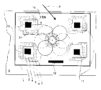
Referring to Figure 1, shown therein is a surface pattern 1 which is applied
in
the form of a security element to a document 2. The surface pattern 1 has N
visually
perceptible patterns which are composed of surface portions or other graphic
elements
with microscopically fine relief structures which have an optical-diffraction
effect, flat
mirror surfaces or absorbent or scattering structures. N is an integer > 0,
and for
CA 02292594 1999-11-30
3
impressive optical motion effects N is selected to be between 6 and 30.
Configurations of the N patterns are described in above-mentioned
specifications EP-
A 105 099, EP-A 330 738, EP-A 375 833 and EP-A 537 439. For considerations
relating to the drawing, Figure 1 shows the N patterns by lines 3 to 7 in
different
forms (by dots, dashes, dot-dashes and so forth). In actual fact an observer
viewing
the surface pattern 1 from the viewing direction 8 perceives in each case only
a single
one of the N patterns in brilliant colours, upon rotation about the line
normal to the
plane of the drawing (shown by the point 9) of the surface pattern 1 when lit
with
daylight; in this example, in the transition from one pattern to the next, the
position of
the visible squares and circles on the surface pattern 1 changes or circles
with the
centre point 9 and involving changing radii are successively visible. Script
images 10
of a corresponding configuration also have the same motion effects.
The N patterns share together at least one independent common surface
element 11 which is not part of the N patterns. A plurality of those surface
elements
11 can be arranged in side-by-side relationship, with or without a spacing,
and form a
band-shaped linear first surface array or configuration 12 of the height of a
surface
element 11. In another embodiment a compact second surface array or
configuration
13 involves the shape of a quadrangle (square, rectangle, rhombus) or another
surface
configuration of any definition. Surface elements 11 which are not
interconnected and
which are delimited in any fashion can be arranged distributed over the entire
surface
pattern 1 or in a loose group.
Figure 2a to 2d show examples of the surface elements 11, in which respect it
is noted here that the illustrated surface elements 11 are shown as rectangles
only for
reasons of representation in the drawing. The surface element 11 is subdivided
into
surface portions 14, 15 and has an arrangement of the surface portions 14, 15,
which
is independent of the N patterns and which is structured in a predetermined
manner
and which is not perceptible with the naked eye, that is to say at least one
dimension
of the surface portions 14, 1 S is smaller than 0.3 to 0.4 mm. Each surface
portion 14
and 15 respectively is occupied with a single, microscopically fine
diffraction
structure or with a structure which has absorbent or scattering properties, or
is a flat
mirror. Hereinafter the structures of the surface portions 14, 15, said
structures not
being specified in greater detail, are identified as the "partial structure".
The surface
CA 02292594 1999-11-30
4
pattern 11 in Figure 2a is subdivided into two equally sized surface portions
14, 15.
The surface portion 14 is occupied by the partial structure "a", while the
surface
portion 15 is occupied by the partial structure "b". The size of the surface
element 11
is for example 0.5 mm wide and 0.6 to 0.8 mm high. For the person viewing the
surface pattern 1 (Figure 1 ) those surface portions 14, 15, if they are
occupied by a
diffraction structure, because of the high level of intensity of the light
diffracted at the
diffraction structure, are visible as striking spots of colour and can
interfere with the
image impression of the respective visible pattern. Damage to the surface of
the
surface element 1 within the surface portion 14 or 15 respectively can
appreciably
reduce the luminous power of the partial structure.
If the surface elements 11 are more finely subdivided, for example as shown in
Figures 2b, 2c and 2d, then the intensity of the surface element 11 decreases,
from the
point of view of the observer. In Figure 2b the surface element 11 is
subdivided with
an arrangement of the inclinedly disposed band-shaped surface portions 14, 15,
16.
The partial structures "a", "b" and "c" are associated with the surface
portions 14, 15
and 16 and form a cyclically changing succession abc abc abc. The smaller
dimension
of the individual surface portions 14, 15, 16 is in the region of 50 pm. If
the partial
structures "a", "b" and "c" are in the form of diffraction structures, they
differ in terms
of at least one grating parameter so that the observer generally sees a mixed
or
secondary colour with less brilliance. In Figure 2c the surface element 11 is
subdivided into regular pixels 17 whose largest dimension does not exceed 0.3
mm.
That arrangement of the cyclically interchanged partial structures "a", "b",
"c" and "d"
in the surface portions 14, 15, 16, 18 is a modification of the arrangement
shown in
Figure 2b, which can be better integrated into one of the known surface
patterns (EP-
A 375 833). Figure 2d shows an arrangement of band-shaped surface portions 14,
15,
at least 30 ~m wide, with the two cyclically interchanged partial structures
"a" and
"b". The examples illustrated here of the arrangement of the partial
structures in the
surface element 11 and the nature of the subdivision of the surface element
are an
incomplete selection.
In Figure 3 the surface pattern 1 (Figure 1) is glued onto the document 2,
with
a layer of adhesive between the laminate 20 and the document 2 providing the
adhesive bond. A relief 19 of the surface pattern 1 includes the surface
portions with
CA 02292594 1999-11-30
the microscopically fine relief structures and with absorbent or scattering
structures or
with planar mirrors of the N patterns and the partial structures of the
surface elements
11. The relief 19 is embedded in a laminate 20 of transparent plastic
material. The
relief 19 can be covered with a reflection layer 21 to enhance the optical
effectiveness.
5 In the region of the surface elements 11, in place of the fine subdivision
into
surface portions 14 (Figure 2a), 15 (Figure 2a), 16 (Figure 2b), it is also
possible to
use a relief structure 19 which is known from WO 97/27504, in which case the
diffractive relief structure 19 is produced from a superposition of
corresponding
simple diffraction gratings and has the same diffraction properties as the
finely
subdivided surface element 11.
Instead of the reliefs 19 which are replicated by embossing and the therefore
completely identical surface patterns 1, it is possible to produce similar
surface
patterns 1 using the technology of the above-mentioned volume holograms 30,
for
example also in the form of individual portions; that procedure is suitable in
particular
for the production of individual security features with individual, machine-
readable
information. The volume hologram 30 is recorded in the form of a pattern of
interferences of coherent reference and object beams in a light-sensitive
layer, the
"foil", which is thick in comparison with the wavelength of the light, wherein
upon
development of the exposed light-sensitive layer in the foil the pattern of
the
interferences involves local changes in the refractive index in the form of
closely
stepped planes arranged in a Venetian blind configuration (_ "fringes"). Those
fringes
act as a light-diffracting structure 30'. As no reflection layer 21 is
required the volume
holograms 30 have inherent transparency. This configuration of the surface
pattern 1
affords the advantage that, after the security feature is glued on the
document 2,
images and text or other indicia of the document 2 still remain visible
through the
volume hologram.
Multiple exposures under different conditions in production of the volume
hologram 30 make it possible to produce in the region of the surface elements
11 in
the same volume a plurality of systems of fringes which act in a similar
manner to the
superimposed relief structures which are known from WO 97/27504.
Machine identification of the document 2 in a reading device which is
described in Swiss application No 1397/97 is advantageous in particular in
relation to
CA 02292594 1999-11-30
6
bank notes and passes of all kinds. In order to permit secure optically
machine
reading, the diffraction structures of the surface elements 11 (Figure 1 ) and
the surface
arrays 12 (Figure 1 ), 13 (Figure 1 ) which are composed thereof have at least
one
spatial frequency fB which is not used in the microscopically fine relief
structures of
the N patterns or an integral multiple of the spatial frequencies fR used for
the relief
structures, that is to say the spatial frequency fB ~ m~fR for m = l, 2, 3,
...; the number
m is the ordinal of the diffraction effect. If diffracted light of the k-th
diffraction order
is detected in the reading device, then selection of the spatial frequency fB
is further
restricted as the exclusion rule k~fB ~ m~fR for m = 1, 2, 3, ... and k = 1,
2, ... must
also apply for that k-th diffraction order. The spatial frequencies fB and fR
are from
the range of 0 to about 3500 lines/mm, that is to say from a planar mirror to
grating
structures which can just still be shaped in the plastic material of the
laminate 20.
It is possible besides the separate spatial frequencies fB and fR also to
provide
separate azimuth regions cp8, cpR for the diffraction structures of the
surface elements
11 and the relief structures of the N patterns.
In the reading device a light source 22 produces monochromatic light 23 of a
predetermined wavelength ~, from the infra-red or visible range of the
spectrum of
electromagnetic waves. The light 23 which is incident on the surface pattern 1
is
diffracted at the large number of surface portions 14 (Figure 2), 15 (Figure
2), 16
(Figure 2), 18 (Figure 2) with the diffraction structures of the spatial
frequency fB; in
this example, in the first diffraction order (m = 1 ). In Figure 3 an arrow 24
specifies
the direction of the light of the wavelength ~,, which is diffracted at the
diffraction
structures. The diffraction structures of the surface portions 14, 15, 16, 18
can differ
by the azimuth cp (0° <_ cp < 360°) and the profile of the
diffraction structure
(symmetrical and asymmetrical gratings, sine, rectangular, triangular and
sawtooth
profile with (f$)-'5 3~~, or (fB)-' >3~~,). The light diffracted at the
surface portions 14,
15, 16, 18 with the same azimuth cp of the diffraction structure is deflected
symmetrically with respect to the incident light 23 and impinges on the
photodetectors
25, 26. The incident light 23 and the two photodetectors 25, 26 arranged
symmetrically with respect to the incident light 23 establish a diffraction
plane 100
CA 02292594 1999-11-30
7
with the azimuth 8 of the surface portions 14, 15, 16, 18 to be detected,
which at the
same time is the plane of the drawing in Figure 3.
The relief structures of the N patterns have other spatial frequencies and for
each pattern another azimuth so that the incident light 23 which is diffracted
at the N
patterns is deflected into other angular ranges r, 1~ which are delimited by
conical
surfaces, and does not reach the photodetectors 25, 26. Those conical surfaces
have as
a common axis the direction of the zero diffraction order; in Figure 3 of the
drawing
that axis is in anti-parallel relationship with the incident light 23.
The reading device in above-mentioned Swiss application No 1397/97, for the
same azimuth 8 (0° <_ 8 < 180°) of the diffraction plane 100
with which a partial
structure is associated, can distinguish at least three states of the
diffracted light, more
specifically diffracted at the symmetrical grating or at one of the two
asymmetrical
gratings with the azimuths cp and cp + 180°. If in contrast the partial
structure has an
absorbent or scattering property or if it is a flat mirror, that involves a
further state
which can be detected by the reading device, "no diffraction structure".
Accordingly
the surface patterns 14, 15, 16, 18 with the same partial structures determine
at least
four states. If for example the surface element 11 contains surface portions
14, 15
with two different partial structures "a", "b" (Figures 2a, 2d), 16 various
states can be
represented with the surface element 11 which serves as an information
element. It is
to be added that in this case two respective photodetectors 25, 26 are to be
arranged in
the reading device in the two diffraction planes 100 corresponding to the
parameters
of the two partial structures "a" and "b". With the information elements, the
identity
of the surface pattern 1 of a document 2 can be encoded and securely detected
with the
reading device. If in a surface element 11 T denotes the number of different
partial
structures which are used in the surface portions 14, 15, 16, 18 and which
respectively
define Z states, the surface element 11 (as information element 29) has E
various
states, wherein E = ZT. If the surface array 12 (Figure 1 ) or 13 (Figure 1 )
includes a
plurality of surface elements 11, for example the number F, then EF various
states of
the information can be theoretically used for optically machine-readable
encoding of
the surface pattern 1.
CA 02292594 1999-11-30
8
The light received by the photodetectors 25, 26 depends inter alia on the
total
surface area of the surface portions 14 and 15 respectively and so forth with
the same
partial structure within the surface element 11. In an example as shown in
Figure 2d
the dimension of the surface element 11 with two partial structures was 0.5 mm
in
width and 1.2 mm in height and the total surface area of each partial
structure was
0.30 mm2. The partial structure was divided in terms of height into 50 pm high
surface portions 14, 15. That gave 12 surface portions 14 with the partial
structure "a"
and an equal number of surface portions 15 with the partial structure "b". The
advantage of this arrangement lies in the virtual impossibility of mechanical
separation of the surface portions 14 and 15 and therefore prevents a surface
element
11 from being assembled together in a fresh configuration from bits, with
fraudulent
intent.
As can be seen from Figure 3, the spatial frequency f$ used in the partial
structure, relative to the spatial frequencies fR of the light-diffracting
relief structures,
involves at least a minimal spatial frequency distance Of, represented by the
arrow 24
in the gap between the two defining conical surfaces of the two angular ranges
I , 1~.
With a typical spatial frequency fB, fR of between 500 and 1000 lines/mm the
spatial
frequency distance Of is about ~f = between 20 and 100 lines/mm.
If the document 2 is a thin paper, for example as in the case of bank notes,
the
laminate 20 follows the rough surface of the paper which often is also
creased. The
light 23 is then locally no longer perpendicularly incident on the surface
pattern 1 and
the direction of the arrow 25 deviates from the reference or target direction
and can
possibly no longer reach the photodetector 25 or 26 respectively. In order to
compensate for those effects, the spatial frequency fB of the diffraction
structure
within the surface portion 14, 15, 16 or 18 respectively involves a modulation
effect,
that is to say the spatial frequency fB does not have an individual value but
varies
within narrow limit values continuously or step-wise, for example between 500
lines/mm and 520 lines/mm with a nominal frequency of fB = 510 lines/mm. The
diffracted light is no longer parallel but slightly divergent, as is indicated
by the
shaded region 27. So that the diffracted light received by the photodetectors
25, 26
CA 02292594 1999-11-30
,' 9
reliably originates from the partial structures, the exclusion rule k~fB ~
m~fR must
apply in respect of all spatial frequencies fB of the modulation range (band
width).
Figure 4 shows an embodiment of the linear surface array or configuration 12.
In an example, the linear surface array or configuration 12 is a succession of
the H
surface elements 11 which are arranged successively in a row. They involve the
arrangement illustrated in Figure 2d of the surface portions 14, 15 or an
arrangement
which is turned through 90° (Pos.S). The parameters of the partial
structures a to e,
which are used in Figure 4, are listed in Table 1. The partial structures "a"
and "c"
allocate the surface elements 11 as being classified in even and odd
positions. The
partial structures "d" and "e" represent the information "logic 0" and "logic
1 ".
Identification of the surface elements 11 by their position in the surface
array or
configuration 12 has the advantage that forgery of the information contained
in the
surface array or configuration 12, by cutting up the surface array or
configuration 12
and re-assembling it, is substantially prevented.
Table 1:
Partial a b c d a
structure
Spatial 1000 per mirror 1000 per 600 per 600 per
plane mm mm
fre uenc mm mm
f$
Azimuth 180 --- 0 180 0
Function odd bit start even bit logic 0 logic 1
character
The surface array or configuration must be optically scanned by a reading
device which reads out sequentially as the information also sticks in the
place value of
the surface elements 11, that is to say in the position thereof in relation to
the start
character (Pos. H=1). The reading device in the drawing of Figure 3 requires
only a
single diffraction plane 100 in which are arranged two pairs of the
photodetectors 25,
26, symmetrically with respect to the incident light 23. The light which is
diffracted
at the two partial structures with the spatial frequencies 600 lines/mm and
1000
lines/mm divides the half space available for the diffracted light of the N
patterns into
three regions and not into two, as shown.
CA 02292594 1999-11-30
The incident light 23 is so deformed by a collimator (EP-A 360 969) that, as
shown in Figure 4, there is formed on the surface element 11 for example an
illuminated surface 28 whose dimension along the surface array or
configuration 12 is
at least 50% of the width of a surface element 11. For reading-out purposes,
the
5 incident light 23 is passed along the linear surface array or configuration
12 in such a
way that one surface element 11 after the other is read out. The start
character permits
clear association of the information elements 29 in the surface array or
configuration
12. The linear surface array or configuration 12 in this example contains the
information "start/O10 ... 11 ". In addition Pos.H can be in the form of a
stop character,
10 wherein the partial structures "b" and "c" clearly signal the stop
character to the
reading device.
The compact second surface array or configuration 13 (Figure 1 ) is shown by
way of example in Figure 5. The surface array or configuration 13 is here
composed
of six surface elements (Figure 2d) which are subdivided with the arrangements
of the
surface portions 14 (Figure 2d), 15 (Figure 2d), wherein the five partial
structures are
combined in the surface elements 11 to give { a, b } , { a, c } , { a, a } , {
b, a } and { c, d } .
Each partial structure establishes one of at least four states. If the entire
surface array
or configuration 13 is simultaneously illuminated, a reading device with three
diffraction planes 100 (Figure 3) and with five pairs of photodetectors 25
(Figure 3),
26 (Figure 3) detects the state which is predetermined by the selected partial
structures, out of 45 = 1024 states. Table 2 contains parameters for a
predetermined
state by way of example.
Without departing from the idea according to the invention, graphic line
elements 31, 32 of the N patterns can extend over the surface of the surface
elements
11 and break it up into the two sub-elements 33 and 34. The association with
the
surface element 11 is determined by the arrangement of the partial structures.
Mutually adjoining surface elements can also be spaced by means of an empty
strip
35. Such line elements 31, 32 are generally extremely narrow (typically
between 30
and 100 pm) and therefore do not interfere with the operation of reading out
the
surface elements 11 or, as Figure 1 shows, the surface arrays or
configurations 12, 13.
CA 02292594 1999-11-30
11
Table 2:
Partial a b c d a
structures
Azimuth
angle of 0 90 0 90 135
the
diffraction
lane
Azimuth 180 270 0 --- 135
an 1e
Diffractionasymmetricalasymmetricalsymmetricalmirror asymmetrical
ratin
Spatial 600 per 600 per 900 per 900 per 900 per
mm mm mm mm mm
fre uenc
fB
Instead of simple strips in the form of a circular ring or a band, a script
image
36 consisting of alpha-numeric characters can also advantageously be selected
for the
surface portions 14, 15, 16, 17, 18, as shown in Figure 6. The alpha-numeric
characters of the script image 36 can have for example the partial structure
"a" and the
background of the characters can have the partial structure "b". In another
embodiment, adjacent script images 36 and the background thereof are separated
by
the surface portion 16 with a third partial structure "c". Such script images
36 with a
height d <_ 0.3 mm and the use thereof are described in EP-A 330 738.
The most important advantages of the encoding set forth herein by means of a
surface array or configuration 12, 13 or a single surface element 11 are
summarised
once again here:
- scratches, dirt, surface flaws and so forth are scarcely noticeable as the
information-bearing partial structures, without having a conspicuous effect,
are
distributed over a relatively large surface element 11;
- the information is encoded exclusively with predetermined spatial
frequencies fB so that the reader can easily read out the information even
from the
surface pattern 1;
- large tolerances in relation to positioning errors of the surface pattern 1
relative to the reading device.