Note: Descriptions are shown in the official language in which they were submitted.
CA 02292859 1999-12-21
DEMODULATOR ARRANGEMENT, METHOD TO DEMODULATE, AND
TELECOMMUNICATION SYSTEM COMPRISING SUCH A DEMODULATOR
ARRANGEMENT
The present invention relates to a demodulator arrangement as defined in
the non-characteristic part of claim l, a method for demodulation of data
symbols performed by such a demodulator arrangement, as defined in the non-
characteristic part of claim 7, and a telecommunication system comprising such
a demodulator arrangement as defined in the non-characteristic part of claim
8.
Such a demodulator arrangement and method to demodulate are already
known in the art , e.g. from the article 'Demodulator With FEC Decoder Has On-
Chip Timing Recovery' from the author Paul McGoldrick. This article was
published on pages 55-64 of the magazine 'Electronic Design' of September 3,
1996. In this article, a family of demodulators is described suitable for
reception
and demodulation of television signals transferred over a cable, for instance
an
optical fibre or coax cable. Data symbols are modulated in the known system in
accordance with a constellation diagram that is shown in Fig. 2 on page 58,
and
that is described via the tables on page 56 of the cited article. The drawn
constellation diagram contains 64 constellation points and has a rectangular
shape. The same constellation diagram evidently is used in the demodulator of
the known system to demodulate received data symbols. The known
demodulator, shown in Fig. 1 of the above mentioned article, contains a fully
coherent detector which determines the amplitude and phase of the data symbols
independently of one another. To be able to accurately determine the amplitude
of the received data symbols, the demodulator includes an automatic gain
control loop which compensates for changes in the amplitude attenuation of the
cable whereover the information is transferred. In addition, to be able to
accurately determine the phase of received data symbols, the known
demodulator includes a timing recovery loop which is described in detail in
the
paragraph 'littering Towards Zero' on the lower half of page 58 of the cited
CA 02292859 1999-12-21
-2-
article. The timing recovery loop has the task to establish a phase reference
for
the incoming information bursts. As will be appreciated by any skilled person
and
as can be understood from the paragraphs 'System Overview' on pages 55-56
and 'littering Towards Zero' on page 58 of the cited article, the automatic
gain
control loop and the timing recovery loop have a significant share in the
hardware complexity of the known television signal demodulator. Moreover, such
a coherent detector typically requires a fairly long acquisition time when
working
in blind acquisition mode. Using a training sequence at the start of everey
information burst may reduce the acquisition time of coherent detectors to a
few
symbols but the current commercially available QAM-receivers are not suited
for
this application.
It is an object of the present invention to provide a demodulator
arrangement suitable to receive and demodulate data symbols transmitted as
part of information bursts over a transmission medium with stable attenuation
characteristics, but whose hardware complexity is significantly reduced in
comparison with that of the known demodulator arrangement and whose
acquisition time is reduced significantly. In addition, it is an object of the
present
invention to provide a related demodulation method and telecommunication
system.
According to the invention, this object is realised by the demodulator
arrangement defined in claim 1, the method to demodulate data symbols
defined in claim 7, and the telecommunication system defined in claim 8.
Indeed, in case bursty information is transferred over a transmission
channel with in time slowly varying attenuation characteristics, coherent
amplitude detection will be successful without the need for an automatic gain
control loop. If the information is transferred over a channel, for instance a
copper twisted pair cable, a coax cable or an optical fibre, whose gain
remains
stable in time, no automatic gain control is required to enable coherent
amplitude detection. It is sufficient that the attenuation of the channel is
measured once at initialisation of the system. On the other hand, by using a
CA 02292859 1999-12-21
-3-
differential phase detector which detects the phase of a data symbol by
measuring the phase difference with the phase of the previously received data
symbol, no timing and/or carrier recovery loops are required in the
demodulator
according to the present invention, although the traffic has a bursty
character.
Differential phase detection is a known technique used in fully differential
demodulator arrangements which are used to detect data symbols sent over
transmission channels with fast varying amplitude and phase characteristics
such
as radio links. Such a fully differential detector for instance is known from
pages
324-327 of the book 'Modern Quadrature Amplitude Modulation, Principles and
Applications for Fixed and Wireless Communications', written by William Webb
and Lajos Hanzo, and published by Pentech Press, London. Summarising,
according to the present invention differential phase detection is combined
with
coherent amplitude detection in a detector used to receive bursty information
transferred over a gain stable link. Thereby, control loops for amplitude and
phase are avoided so that the demodulator's hardware complexity is reduced
significantly.
It is to be noticed that the term 'comprising', used in the claims, should
not be interpreted as being limitative to the means listed thereafter. Thus,
the
scope of the expression 'a device comprising means A and B' should not be
limited to devices consisting only of components A and B. It means that with
respect to the present invention, the only relevant components of the device
are A
and B.
Similarly, it is to be noticed that the term 'coupled', also used in the
claims, should not be interpreted as being limitative to direct connections
only.
Thus, the scope of the expression 'a device A coupled to a device B' should
not
be limited to devices or systems wherein an output of device A is directly
connected to an input of device B. It means that there exists a path between
an
output of A and an input of B which may be a path including other devices or
means.
CA 02292859 1999-12-21
-4-
In a particular embodiment of the present invention, a large constellation
scheme is used as defined in claim 2.
An additional feature of the present invention is defined in claim 3.
In this way, by using a circular constellation diagram wherein phases are
distributed equidistantly and wherein amplitude levels are equidistant,
robustness
for noise of the coherent amplitude, differential phase detector according to
the
present invention is minimised.
A further feature of the demodulator arrangement according to the
present invention is defined in claim 4.
In this way, by using a so called staggered constellation diagram instead
of a linear constellation diagram, the distance between constellation points
is
increased which even more improves robustness for noise.
Furthermore, an embodiment of the present invention is adapted for
upstream transmission in a time multiplexed way over a hybrid fibre coax
network as defined in claim 5.
Indeed, the hybrid optical fibre/coaxia) cable transmission medium of a
hybrid fibre coax network has a stable gain in time. Moreover, because the
medium is shared in a time division multiplexed way, upstream transmission
occurs in bursts which makes applicability of the present invention to hybrid
fibre
coax systems very suitable.
Alternatively, an embodiment of the present invention is adapted for
downstream transmission in an hybrid fibre coax system, as defined by claim 6.
The above mentioned and other objects and features of the invention will
become more apparent and the invention itself will be best understood by
referring to the following description of an embodiment taken in conjunction
with
the accompanying drawings wherein:
Fig. 1 a drawing illustrating the architecture of a hybrid fibre coax system
wherein an embodiment of the present invention is used;
Fig. 2 shows the constellation diagram used in the system of Fig. 1 for
modulation and demodulation of data symbols; and
CA 02292859 1999-12-21
-5-
Fig. 3 is a functional block scheme of an embodiment of the demodulator
arrangement according to the present invention, used in system of Fig. 1.
The hybrid fibre coax system drawn in Fig. 1 includes a head end station
HE, an optical network termination ONT and four terminals TA, TB, TC and TD.
The head end station HE is coupled via a bi-directional optical fibre link to
the
optical network termination ONT and the latter optical network termination ONT
is coupled to the terminals TA, TB, TC and TD via a common coax link and
respective individual coax links, which are also suitable for bi-directional
transmission. The upstream and downstream directed signals occupy different
frequency bands on the optical fibre and coaxial links of the hybrid fibre
coax
system.
In the upstream direction, i.e. the direction from the terminals TA, TB, TC
and TD to the head end station HE, the terminals TA, TB, TC and TD send data
packets which share the common coax link towards the optical network
termination ONT in a time multiplexed way. The data packets A1 and A2 thus
occupy timeslots assigned after a ranging procedure performed at
initialisation of
the system to the terminal TA. Similarly, the data packets B1 and B2 occupy
timeslots assigned to the terminal TB, data packets C1 and C2 occupy timeslots
assigned to the terminal TC, and data packets Dl and D2 occupy timeslots
assigned to the terminal TD. The optical network termination ONT is
responsible
for the electro/optical conversion of the upstream transferred data packets
A1,
Bl, C1, D1, A2, B2, C2, D2 and the so generated optical signal is transmitted
at
a high bitrate towards the head end station HE. In the head end station HE,
the
optical signal is opto/electrical converted and the so generated data packets
are
applied to a demodulator arrangement, according to the present invention. For
amplitude and phase demodulation of the data symbols that constitute the data
packets, the demodulator arrangement in the head end station HE uses the
constellation scheme of Fig. 2. The structure of this demodulator arrangement
is
illustrated by Fig. 3.
CA 02292859 1999-12-21
-6-
In the downstream direction, i.e. the direction from the head end station
HE to the terminals TA, TB, TC and TD, the head end station HE broadcasts
information after modulation and electro/optical conversion thereof. This
information stream is opto/electrical converted in the optical network
termination
ONT and further broadcasted over the coaxial network towards the terminals TA,
TB, TC and TD. The downstream broadcasted information stream, which after
receipt is demodulated in the terminals TA, TB, TC and TD, is not illustrated
in the
figure Fig. 1. To be able to demodulate the downstream broadcasted information
stream, the terminals TA, TB, TC and TD are each equipped with a demodulator
arrangement according to the present invention. The constellation scheme used
by this demodulator arrangement is drawn in Fig. 2, and the structure of this
demodulator arrangement is again that of Fig. 3. In other words, the pure
theoretical system drawn in Fig. 1 uses the same constellation scheme for
upstream and downstream transmission and the same demodulator
arrangement for demodulation of the upstream and downstream transmitted
information.
For the demodulator arrangements in the head end station HE and the
terminals TA, TB, TC and TD, it is assumed that the amplitude of the received
signals is known. This amplitude knowledge may be obtained by a ranging
technique, performed during initialisation of the system, or via a look-up
table. In
a similar way, it is assumed that the symbol timing is known for received
signals
in the head end station HE as well as in the terminal stations TA, TB, TC and
TD.
This symbol timing knowledge also may be obtained by a ranging technique or
alternatively, via a look-up table. Another assumption is that the carrier
frequency
of the upstream or downstream transmitted signals is not exactly known by the
receiver and the carrier phase is not at all known. This carrier phase is
affected
by noise from tuners on top of white Gaussian noise. Every upstream channel
moreover may be supposed to be equipped with an equaliser with slowly varying
settings that are tuned via a separate training cycle. Since equalisation is
not the
CA 02292859 1999-12-21
subject of the present invention, no more details will be given with respect
thereto
in the remainder of this application.
The demodulator arrangement incorporated in the head end station HE of
Fig. 1 for demodulation of upstream transferred information and incorporated
in
the terminals TA, TB, TC and TD for demodulation of downstream broadcasted
information, uses the constellation scheme of Fig. 2 for demodulating data
symbols. This circular constellation scheme contains 32 constellation points
distributed over 4 amplitude levels, A1, A2, A3 and A4, with equidistant
amplitudes: B, B+A, B+2A and B+3A. The constellation points can have 8
different phases, P1, P2, P3, P4, P5, P6, P7 and P8, which are also
equidistantly
distributed. The constellation points are so labelled that their label is
indicative
for both their amplitude level and their phase: A1 P1, A1 P2, A1 P3, Al P4, A1
P5,
A 1 P6, A 1 P7, A 1 P8, A2 P 1, A2 P2, A2 P3, A2 P4, A2 P5, A2 P6, A2 P7, A2
P8, A3 P 1,
A3P2, A3 P3, A3 P4, A3P5, A3P6, A3P7, A3P8, A4P1, A4P2, A4P3, A4 P4, A4 P5,
A4P6, A4P7 and A4 P8. The constellation is thus based on equidistant circles
on
which the constellation points are placed on angles, equally spaced from one
another. The matrix of amplitudes and phases is always full, i.e. the number
of
phases on each circle is equal. It is noticed that it could be seen as
advantageous
to define, as an alternative for the constellation diagram of Fig. 2, a number
of
inner circles with a small radius whereon less constellation points are put.
However, for differential phase detection, this has nearly no advantage since
the
uncertainty on the differential phase is dependent mainly on the worst case,
i.e.
the inner points. So, not much more constellation points can be placed on the
larger circles because the uncertainty on the differential phase still
requires a
large phase difference, also between the outer points. For this reason, only
constellations with a completely filled combination of amplitudes and phases
are
considered here.
It is assumed that the modulation is quasi optimal when for every
constellation point, the closest distance to a region in the constellation
diagram
associated with an adjacent constellation point shows a flat distribution,
with all
CA 02292859 1999-12-21
_g_
values higher than but as close as possible to a threshold value. If the
instantaneous noise voltage remains smaller than this minimal distance value,
no
bit error will occur. Under this condition, the ratio between the square of
this
maximal noise voltage and the average received power determines the signal to
noise ratio for a certain bit error rate.
Regions in the constellation diagram with an equal chance of being
reached by white noise from a certain constellation point are named here
equiprobable error regions. In the amplitude direction, the equiprobable error
region is simply determined by the Gaussian noise power. In the phase
direction,
the worst case for differential detection occurs when the differential phase
is
measured between a constellation point closest to the origin and any other
point.
For points far away from the origin, the equiprobable error region for
differential
detection will be strongly extended in the phase direction. For the
calculations, it
is assumed that the equiprobable error region in the phase direction is given
by
the root of the sum of the squares of the phase equiprobale error region of
the
constellation point under study, combined with a constellation point closest
to the
origin. For large constellations under differential detection, this means that
the
outer constellation points must be spaced far away in the phase direction,
since
they can always be combined with an inner point, showing a much larger noise
on the phase. This explains the inherent loss of signal to noise budget under
differential detection on large constellations: the inner region cannot be
used
because it would cause a large noise on the differential phase of all other
points
in the diagram and the outer points cannot be placed optimally close to one
another in the phase direction because their phase accuracy is strongly
reduced
by differential detection with an inner point.
In the light of the above made assumptions, three noise sources have an
effect on the equiprobable error regions: white Gaussian noise, phase noise
and
amplitude uncertainty. White Gaussian noise results in a circular region of
equiprobable error in the I-Q plane of Fig. 2, phase noise results in an
extension
of the equiprobable error regions in phase direction, and amplitude
uncertainty
CA 02292859 1999-12-21
-9-
of the received signal results in an extension of the equiprobable error
region in
the amplitude direction. The most suitable constellation diagram, i.e. the one
that
provides the best noise robustness, is a diagram with equidistant phases and
equidistant amplitude levels for the constellation points.
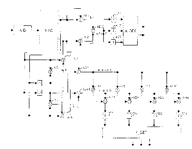
The demodulator arrangement drawn in Fig. 3 includes an analogue to
digital converter A/D, a Nyquist filter NYQ, a first and second multiplier M1
and
M2, a first adder AD1, a first, second and third amplitude threshold
comparator
ATI, AT2 and AT3, an amplitude detector A_DET, a third, fourth, fifth and
sixth
multiplier M3, M4, M5 and M6, a subtractor SUB1, a second adder AD2, a first
and second delay unit D1 and D2, a seventh, eight, ninth, and tenth multiplier
M7, M8, M9 and M10, a third, fourth, fifth and sixth adder AD3, AD4, AD5 and
AD6, a first, second, third and fourth phase threshold comparator PT1, PT2,
PT3
and PT4, and a phase detector P-DET.
The analogue to digital converter A/D and Nyquist filter NYQ are cascade
coupled to an input terminal of the demodulator arrangement, the Nyquist
filter
NYQ having two output terminals. These two output terminals of the Nyquist
filter
NYQ serve as inputs for a coherent amplitude detecting arrangement on the one
hand and a differential phase detecting arrangement on the other hand. The
amplitude detecting arrangement contains the parallel coupling of the first
multiplier M1, connected with its two inputs to the first output terminal of
the
Nyquist filter NYQ, and the second multiplier M2, connected with its two
inputs to
the second output terminal of the Nyquist filter NYQ . the outputs of the
first
multiplier Ml and the second multiplier M2 are connected respectively to a
first
input terminal and a second input terminal of the first adder ADD1, and the
latter
first adder ADDI is connected via its output terminal to inputs of the first,
second
and third amplitude threshold comparator AT1, AT2 and AT3. The first amplitude
threshold comparator ATl has an output coupled to a first input of the
amplitude
detector A_DET, the second amplitude threshold comparator AT2 has an output
coupled to a second input of the amplitude detector A-DET, and the third
amplitude threshold comparator AT3 has an output coupled to a third input of
CA 02292859 1999-12-21
-~0-
the amplitude detector A_DET. The amplitude detector A-DET is equipped with
two output terminals which serve as outputs for the whole demodulator
arrangement. The above mentioned phase detecting arrangement is coupled
parallel with the just described amplitude detecting arrangement to the two
output terminals of the Nyquist filter NYQ. The third multiplier M3 has two
inputs
whereto respectively the first output terminal of the Nyquist filter NYQ is
connected, and the second output of the Nyquist filter NYQ is coupled via the
first
delay unit Dl. The fourth multiplier M4 has two inputs whereto respectively
the
second output of the Nyquist filter NYQ is connected and the first output
terminal
of the Nyquist filter NYQ is coupled via the second delay unit D2. The fifth
multiplier M5 has two inputs whereto respectively the first output of the
Nyquist
filter NYQ is connected and the first output terminal of the Nyquist filter
NYQ is
coupled via the second delay unit D2. The sixth multiplier M6 has two inputs
whereto respectively the second output of the Nyquist filter NYQ is connected
and
the second output terminal of the Nyquist filter NYQ is coupled via the first
delay
unit Dl . Output terminals of the third multiplier M3 and fourth multiplier M4
are
connected to input terminals of the subtractor SUB1, and this subtractor SUBI
is
with its output terminal connected to first inputs of the third, fourth, fifth
and sixth
adder AD3, AD4, AD5 and AD6. Output terminals of the fifth multiplier M5 and
the sixth multiplier Mb are connected to input terminals of the second adder
AD2,
and the output terminal of this second adder AD2 is coupled via the seventh
multiplier M7 to the second input of the third adder AD3, via the eight
multiplier
M8 to the second input of the fourth adder AD4, via the ninth multiplier M9 to
the second input of the fifth adder ADS, and via the tenth multiplier M10 to
the
second input of the sixth adder AD6. The third adder AD3 is coupled with its
output to a first input terminal of the phase detector P_DET via the first
phase
threshold comparator PTI, the fourth adder AD4 is coupled with its output to a
second input terminal of the phase detector P_DET via the second phase
threshold comparator PT2, the fifth adder AD5 is coupled with its output to a
third input terminal of the phase detector P_DET via the third phase threshold
CA 02292859 1999-12-21
comparator PT3, and the sixth adder AD6 is coupled v~~ith its output to the
fourth
input terminal of the phase detector P-DET via the fourth phase threshold
comparator PT4. The phase detector P_DET is equipped with three output
terminals which serve as third, fourth and fifth output terminals for the
whole
demodulator arrangement.
The proposed constellation is based on a separate detection of the
amplitude and the differential phase. The amplitude is detected on an absolute
scale, since the amplitude is controlled by a ranging circuit or is controlled
by a
look-up table in the receiver. The phase is detected differentially compared
to the
previous constellation point. For a DSP (Digital Signal Processing)
implementation, the square of the amplitude is found as the sum of the square
of
the real and imaginary parts of the currently received data symbol. The
differential phase is found by a complex division of the current and the
previous
data symbol. Using a number of thresholds on the values of amplitude and
phase gives the resulting bit pattern. How this principle is realised by the
demodulator drawn in Fig. 3 is explained in detail in the following paragraph.
The incoming signal of the demodulator of Fig. 3 is digitised by the
analogue to digital converter A/D and filtered by the Nyquist filter NYQ. Each
digital data symbol at the output of the Nyquist filter NYQ corresponds to a
point
in the I-Q plane of Fig. 2 and to a complex number with a real and imaginary
part. The real parts of successive data symbols are sourced via the first
output of
the Nyquist filter NYQ and the imaginary parts of the successive data symbols
are sourced via the second output of the Nyquist filter NYQ. The amplitude
detecting arrangement has the task to detect on which one of the four circles
of
the constellation diagram of Fig. 2, the point that corresponds to the
incoming
data symbol is laying. The amplitude detecting arrangement thereto determines
the square of the amplitude of the complex number b,+j.b; sourced by the
Nyquist filter NYQ and compares this square amplitude with three thresholds.
The first multiplier Ml calculates the square b~2 of the real part b~ of a
received
data symbol, the second multiplier M2 calculates the square b;2 of the
imaginary
CA 02292859 1999-12-21
-12-
part b; of the received data symbol, and the first adder ADl calculates the
square
amplitude b,2+b;2. The first, second and third amplitude threshold comparators
ATl , AT2 and AT3 determine whether the square amplitude b,2+b;2 is lower than
or higher than three t! hold values which are chosen so as to distinguish
points
on the four circles of Fig. 2 from each other, even when affected by noise.
The
amplitude detector A_DET determines on the basis of the output of the
amplitude
threshold comparators ATI, AT2 and AT3 on which circle the received
constellation point is laying and derives therefrom two bits of the data
symbol.
The phase detecting arrangement has the task to detect the phase of the
received
constellation point and has to map this phase to one of the eight possible
phases
in the constellation diagram of Fig. 2. The phase detecting arrangement
thereto
divides two successive complex numbers, b,+ib; and a~+ja;. Indeed, the complex
number c,+jc; obtained by dividing b,+jb; by a,+ja; is equal to
(a~.b~+a;.b;)/(a,2+a;2) + j(a~.b;-a;.b~)/(a~2+a;2) and has a phase equal to
the
difference in phase between the complex numbers ar+ja; and b~+ib;. the complex
number c,'+jc;' equal to (a,.b,+a;.b;) + j(a,.b;-a;.b,) has the same phase as
the
complex number cr+jc; since it is proportional thereto with a factor a,2+a;2.
The
phase detecting arrangement of Fig. 3 thus starts from the two successive data
symbols a,+ja; and b,+ib; to calculate c,'+jc;' and then compares the phase of
c~'+jc;' with four phase thresholds to derive therefrom the 3 remaining bits
modulated on the data symbol. The third multiplier M3 calculates a~.b; and the
fourth multiplier M4 calculates a;.b,. The output a;.b~ of multiplier M4 is
subtracted from the output ar.b; of multiplier M3 by the subtractor SUBI which
so
produces c;'. The fifth multiplier M5 calculates a~.b~ and the sixth
multiplier M6
calculates a;.b;. The output a~.b~ of the fifth multiplier M5 and the output
a;.b; of
the sixth multiplier M6 are added together by the second adder AD2 which so
produces c,'. The real part c,' and imaginary part c;' are shifted in phase
over 90
degrees vis-a-vis each other by the multipliers or mixers M7, M8, M9 and M10.
The third adder AD3, the fourth adder AD4, the fifth adder AD5 and the sixth
adder AD6 afterwards constitute from c,' and c;' the complex number c,'+jc;'
and
CA 02292859 1999-12-21
-13-
the four phase threshold comparators PT1, PT2, PT3 and PT4 compare the phase
of c,'+jc;' with four phase threshold values to derive therefrom to which one
of
the eight possible values, 0, ~/4, n/2, 3~/4, n, 5n/4, 3~t/2, 7n/4 or 2n
radians,
this phase is equal. The so obtained phase from c~'+jc;' is equal to the phase
difference between a,+ja; and b,+jb;. If the phase detector P_DET knows the
phase of the previous data symbol a,+ja;, it can calculate from the output
signals
of the four phase threshold comparators PTI, PT2, PT3 and PT4 the phase of the
successive data symbol b~+jb;. This phase then determines the three remaining
bits of the data symbol. Together with the two bits at the output of the
amplitude
detector A-DET, the three outputs of the phase detector P_DET constitute the
demodulated data symbol.
A first remark is that two methods of placing the points on circles may be
considered: linear, as illustrated by Fig. 2, and staggered. In the linear
filling, the
phase on the circles with even index and odd index is the same. In the
staggered
filling, the phases of points on the circles with even index is half a step
offset in
comparison with the phases of points on the circles with odd index. In this
way, a
somewhat larger distance is created between the constellation points. For the
detection of linear constellations, the dete~+~~n of phase and amplitude is
completely independent. The detection of the amplitude bits requires a number
of
thresholds, one less than the number of amplitude levels, as was illustrated
above by the embodiment with three amplitude thresholds and four amplitude
levels. The detection of the differential phase requires approximately loge of
the
number of phase steps. For the detection of staggered constellations, twice
the
number of thresholds is required in the amplitude direction and twice the
number
of phase states must be detected. A truth table is required there for looking
up
the combinations of amplitude and phase that lead to correct values associated
with a constellation point. It must be considered that a staggered
constellation
needs a more complex receiver architecture than the one drawn in Fig. 3. For
the
staggered constellations, two threshold amplitude levels are defined per
circle.
CA 02292859 1999-12-21
-14-
These allow a better confinement of the occupied area in the constellation
diagram to the equiprobable error region ellipse.
The parameters to optimise when selecting a constellation are the number
of circles and the radius of each circle and the number of phase levels (only
constellations with an equal number of points per circle a~ a considered). The
value to be optimised is the ratio between the square of the maximal allowed
noise voltage a2 (i.e. the noise power) over the average power E of the
constellation (i.e. the signal power), under the boundary condition that the
equiprobable error regions of all points do not overlap. This figure of 62/E
is the
figure of merit for the constellation. Lab test have shown that the gain in
noise
power over signal power achieved by using staggered constellations instead of
linear constellations always remains less than 0.6 dB. In a cable environment,
it
seems that the additional implementation complexity of staggered
constellations
is not worth this small gain, at least not as long as intermodulation does not
impose very stringent power limitations.
It is noticed that although the above described embodiment of a
demodulator arrangement according to the present invention is used in a hybrid
fibre coax system, applicability of this invention is not limited to
telecommunication systems wherein the physical links are constituted by
optical
fibres or coaxial cables. In fact, the demodulator arrangement according to
the
present invention is optimal for use in systems wherein the physical
transmission
medium has slowly varying amplitude characteristics, like twisted pair copper
cables, coaxial cables, optical fibres, ..., and wherein the carrier frequency
is not
exactly known at the receiver, for instance because of the bursty nature of
the
transmission like in upstream hybrid fibre coax systems. The slowly varying
amplitude characteristics justify the coherent amplitude detection, whereas
the
unknown carrier frequency justifies the differential phase detection.
Another remark is that an embodiment of the present invention is
described above in terms of functional blocks. From the functional description
of
these blocks it will be obvious for a person skilled in the art of designing
CA 02292859 1999-12-21
electronic devices how embodiments of these blocks can be manufactured with
well-known electronic components. A detailed architecture of the contents of
the
functional blocks hence is not given for most of them.
While the principles of the invention have been described above in
connection with specific apparatus, it is to be clearly understood that this
description is made only by way of example and not as a limitation on the
scope
of the invention.