Note: Descriptions are shown in the official language in which they were submitted.
CA 02293029 1999-12-20
Doc. No. 10-136 CA Patent
Method and Device for Controlling the Polarization of a Beam of Light
Field of the Invention
This invention relates to devices for controlling polarization of incident
optical signals
and, more particularly, to devices which permit endless or reset-free
operation.
Background of the Invention
Optical signals in standard, non-polarization preserving optical fibre-based
communication systems experience random changes in polarization state from one
end of
the fibre to the other due to fibre birefringence induced by temperature
fluctuations and
physical stresses on the fibres. Random polarization changes are evidenced at
the output
end as polarization dependent loss (PDL) and in some instances polarization
mode
dispersion (PMD).
In order to correct the polarization state of lightwave signals emerging from
the optical
fibre transformers have been developed to transform the fibre output
polarization into the
prescribed polarization state for applications such as heterodyne detection
and
2o interferometric signal processing. Conventional polarization transformers
provide
compensation but require a reset cycle when their operating range is exceeded.
Unfortunately, reset cycles give rise to periods of unacceptable data loss.
Endless
polarization transformers provide continuous control of the polarization state
over an
infinite range of polarization compensation.
Endless polarization transformers have been developed using cascaded
polarization
transformers having a limited transformation range such as fibre squeezers and
electrooptic devices using lithium niobate or PLZT. While these cascaded
devices permit
truly endless (reset free) operation, individual elements within the devices
still require
occasional reset cycles. Although the reset cycles can be performed without
affecting the
overall polarization transformation (quasi-endless polarization control),
these devices
CA 02293029 2004-04-28
Doc. No. 10-136 CA Patent
generally fail to permit polarization control during reset cycles. Moreover,
they require
sophisticated and even computer controlled drive algorithms for proper
operation.
Fibre squeezers mechanically induce birefringence in the fibre axes to cause
retardation
between the two orthogonal modes perpendicular and parallel to the direction
of pressure.
United States Patent number 5,561,726 in the name of Yao, describes a system
that
utilizes a rotatable fibre clamp to supply the necessary retardation and
optical axis
orientation. Although this device can be used for fixed wavelength and
temperature and
polarization it cannot be used to control real time polarization fluctuation
in transmission
fibres, because it requires mechanical movement for its control.
Recently, a reset-free, endless polarization transformer was demonstrated
performing
general polarization transformations from any arbitrarily varying optical
input
polarization into any arbitrarily output polarization by producing adjustable
elliptical
birefringence of constant total phase retardation in a single-mode waveguide.
See U.S.
Pat. No. 4,966,431 issued to Heismann on Oct. 30, 1990. A particular
transformation is
obtained by adjusting the azimuth of linear birefringence and the ratio of
linear to circular
birefringence. In its integrated-optic realization, the endless polarization
transformer
includes at least one cascadable transformer section comprising cascaded first
and second
TE TM mode converters. Phase shifting (TE/TM) is performed in a section
between the
mode converters, in a section following the mode converters, or both between
and
following the mode converters. All sections are formed over a birefringent
waveguide
capable of supporting propagation of TE and TM optical signal modes. While the
recent
endless, reset-free polarization transformer is cascadable and affords
simplicity of design
and operation over prior art devices, it cannot be overlooked that this
polarization
transformer has a relatively narrow optical bandwidth at wavelengths of
interest less than
1 ntn at 1.55 .pm and permits only limited tunability over a small wavelength
range
approximately 10 nm.
Heismann in United States Patent number 5,212,743 entitled Automatic
Polarization
Controller Having Broadband Reset-Free Operation discloses a wide optical
bandwidth
CA 02293029 2004-04-28
Doc. No. 10-136 CA Patent
and broad wavelength tuning range achieved in a reset-free, optical, automatic
polarization controller by combining three controllable fractional wave
elements in
cascade and further by controlling the orientations of both outermost
fractional wave
elements to differ by a prescribed angular amount which is maintained
substantially
constant. Synchronous control of both outermost fractional wave elements
maintains the
prescribed angular difference may be maintained constant during operation of
the
polarization controller.
In the embodiments described by Heismann, the three fractional wave elements
are
provided in the form of an endlessly rotatable half wave element and two
synchronously
rotatable quarter-wave elements wherein the half wave element is placed
between the
quarter-wave elements. Each fractional wave element varies the orientation of
retardance
along its optical wavepath and introduces a specified phase retardation.
Embodiments of
the polarization controller are realized using either distributed bulk optic
devices or
integrated electro-optic waveguide devices. Rotation of the elements is
afforded by a
feedback control circuit which monitors the output optical polarization and
derives
appropriate electrical drive signals to achieve the proper rotation of the
elements.
Although the device taught by Heismann appears to achieve its intended
function in
many instances it does not provide suitable wavelength and temperature
independence.
It is an object of this invention to provide an automatic polarization
controller having
broadband operation wherein undesired reset operations are obviated and which
is
relatively wavelength and temperature independent.
It is a further object of the invention to provide an inexpensive, highly
responsive device
for controlling polarization of an input beam of light having varying
polarization states.
Summary of the Invention
In accordance with the invention, a device for varying or maintaining the
polarization of
an input beam of light is provided comprising:
CA 02293029 1999-12-20
Doc. No. 10-136 CA Patent
a block of electro-optic material having terminals for applying voltages Vx
and Vy across
the block, the block having an input end for receiving the input beam; and,
a controller for controlling the voltages Vx and Vy to a first and a second
pair of
electrodes, the voltages Vx and Vy having the form of a magnitude component
and an
angular component such that the angular component of the voltages Vx and Vy is
varied
in such a manner as to orient an electric field within the electro-optic
material between
the pair of electrodes through a plurality of angles, and such that the
magnitude
component of the voltages is varied to yield a variable phase retardation .
to In accordance with the invention a system is provided for varying or
maintaining the
polarization state an input beam of light for any given polarization state
comprising:
a block of electro-optic material having two pairs of electrodes for applying
a voltages
Vx and Vy in quadrature, the block having an input end for receiving the input
beam;
and,
a controller for controlling voltages applied in quadrature to a first and a
second pair of
electrodes, the quadrature voltages having the form of VosinO and VocosO, the
controller
for varying magnitude Vo and an angle 0 such that the applied voltages are
varied in such
a manner as to orient an electric field within the electro-optic material
between the pairs
of electrodes through a plurality of angles from 0 to y radians and, the
controller for
2o varying the magnitude Vo of the applied voltages to yield a retardation 0
to x , wherein
one of x and y are equal to at least 2~ radians and the other of x and y are
equal to at least
~c radians.
In accordance with another aspect of the invention a method of varying the
polarization
of an input beam of light is provided comprising the steps of:
a) providing two pairs of electrodes disposed about an electro-optic material;
b) passing the input beam of light through the electro-optic material; and,
c) providing a plurality of different quadrature voltage values, each voltage
value having
a magnitude component Vo and an angular component 8 to each of the two pairs
of
3o electrodes wherein both the magnitude component Vo and angular component 0
differ
between some of the plurality of quadrature voltages provided.
4
CA 02293029 1999-12-20
Doc. No. 10-136 CA Patent
In accordance with another aspect of the invention a method of varying the
polarization
of an input beam of light is provided comprising the steps of:
a) providing two pairs of electrodes disposed about an electro-optic material;
b) passing the input beam of light through the electro-optic material; and,
c) providing a plurality of different voltage values, each voltage value
having a
magnitude component and an angular component to each of the two pairs of
electrodes
wherein both the magnitude component and angular component differ between some
of
the plurality of voltage values provided.
to
Advantageously, this invention requires only a single stage and only two
control
parameters, providing simpler control than prior art devices and endless
polarization
tracking.
Brief Description of the Drawings
Exemplary embodiments of the invention will now be described in conjunction
with the
drawings in which:
Fig. 1 is a diagram of a prior art polarization control circuit utilizing two
quarter wave
2o plates and one half wave plate.
Fig. 2 is diagram of a portion of the conventional polarization modulator
wherein a single
pair of electrodes coupled to a block of electro-optic material;
Fig. 3 is a graph of retardance vs. applied voltage simulated for different
temperatures
from 0 degrees C, to 100 degrees C based on the Sellemeier Temperature
Dependent
equations for the ordinary and extra-ordinary indices for the device of Fig.
2;
Fig. 4 illustrates the birefringence ellipse of the transverse device of Fig.
2 which is
always oriented with it's major and minor axes in the x and z directions;
Fig. 5 is a device in accordance with the invention wherein an electro-optic
crystal is
biased across its x and y axis and is oriented such that light launched into
one end
propagates along its z-axis;
5
CA 02293029 1999-12-20
Doc. No. 10-136 CA Patent
Fig. 6 illustrates the incoming light in accordance with the device of Fig. 5,
wherein the
radius is equal to the ordinary index and wherein, there is no retardance when
no voltage
is applied to the crystal unlike the previous transverse device shown in Fig.
4;
Fig. 7 is a graph which indicates that the orientation of the birefringence
ellipse is
independent of the applied voltage (Vo), and is independent of the
temperature;
Fig. 8 is a graph which indicates that the retardance is not dependent upon
temperature;
Fig. 9 is a graph which indicates that the retardance is not dependent upon
the angle 8.
Fig. 10 is a prior art analog control circuit;
Fig. 11 is a digitally controlled control circuit in accordance with the
invention; and,
to Fig. 12 is a diagram illustrating how an effective reset-free operation is
achieved.
Detailed Description
Referring now to Fig. 1, a prior art polarization controller is shown wherein
three fixed
wave-plates are provided each having a pair of electrodes to which a modified
quadrature
voltage is applied.
In Fig. 2 a transverse electric field is applied, in the direction of the
crystal axis (z-axis),
to fully exploit the large electro-optic coefficient by biasing two electrodes
at opposing
2o sides of the wave-plate 10. When zero volts is across the two electrodes
12a and 12b,
there is a natural refractive index difference ~n of approximately
0.083:between the
ordinary and extraordinary axis of the electro-optic material. For a crystal
length L of
approximately SOmm and thickness d of lmm, this introduces about 4720
retardance
between orthogonal polarization components. By applying a non-zero Vz,
additional
birefringence is introduced, which is dependent on the aspect ratio d/L, and
the applied
voltage Vz. Unfortunately, there is also significant temperature dependence
for this
device. The graph of Fig. 3 shows a 'Retardance vs. Applied Voltage'
relationship
simulated for different temperatures from 0 degrees C, to 100 degrees C based
on the
Sellemeier Temperature Dependent equations for the ordinary and extra-ordinary
indices.
6
CA 02293029 2004-04-28
Doc. No. 10-136 CA Patent
Fig. 4 illustrates the birefringence ellipse of the transverse device of Fig.
2 which is
always oriented with it's major and minor axes in the x and z directions; i.e.
the
birefringence ellipse never rotates about the optical axis. Therefore this
device is useful
as a variable polarization retarder, if the temperature of the crystal can be
kept constant,
and if the penalty associated with biasing the device at a voltage at the zero-
retardance
point is acceptable.
In accordance with this invention, and referring to Fig. 5, a device 55
includes a crystal
50 having a length L and a depth d being biased across electrodes 52a, S2b,
and S4a and
54b. Voltage sources Vx and Vy provide quadrature voltages to the device 55.
Electrooptically the crystal 50 behaves as a waveplate. Applied voltage
generates an
electric field across the axis of the crystal 50 and the electric field
creates a refractive
index change along that full crystal length of that axis.
Fig. 5 illustrates a rotatable variable retardance waveplate having a length L
which in
this exemplary embodiment is 100mm. Incoming light enters a GRIN lens and is
collimated through the 1 x 1 x 1 OOmm LiNb03 crystal length, and is
subsequently
refocused back into an output fibre. The crystal 50 is metalized with
electrodes 52a,
52b, and 54a and 54b on all four long sides. These are electrically isolated
from each
other,
The length of the waveplate should be selected in accordance with the
magnitude of the
applied voltatge Vo for a particular desired retardance to maintain a constant
voltage
length product. For example, a longer crystal requires a smaller maximum value
of Vo.
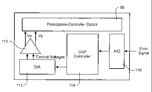
Control circuitry for controlling the rotatable variable retardance waveplate
is well
known, for example Fig. 10 is a prior art circuit of Heismann United States
Patent
5,211,743 which illustrates a control circuit. Fig. 11 shows a control circuit
in accordance
with this invention wherein a digital signal processor (DSP) 114 provides
values to a
digital to analog (D/A) converter 112 which provides control voltages to an
amplifier
110. Output terminals of the amplifier Vx and Vy are coupled directly to the
terminals of
the crystal where the voltage is applied. Control is maintained by way of an
error feed-
CA 02293029 1999-12-20
Doc. No. 10-136 CA Patent
back signal which is provided to the DSP 114 by way of an analog-to-digital
(A/D)
converter 116.
With applied voltage in quadrature the crystal 50 will function as a fully
rotatable
arbitrary retardance wave plate.
In operation, an in a preferred embodiment, voltage is applied in quadrature
to the
electrodes 12a, 12b and 14a, such that:
1o Vx = Vo sin(0)
Vy = Vo cos(9)
The voltages Vx and Vy each have a magnitude portion Vo and an angular
component 8.
The angle 8 is variable from 0 to 2~ and the voltage Vo is variable and can
attain values
which yield up to 2~ or more retardance. For a crystal having a length of
100mm and a
width of 1 mm the required voltage Vo to achieve 2~ retardance voltage is
approximatley
260V. Varying 0 causes the crystal's fast axis to be effectively rotated by
0/2.
With zero volts (i.e. Vo = OV), the birefringence ellipse seen in Fig. 6 by
the incoming
light is a circle, of radius equaling the ordinary index. Hence, there is no
retardance when
no voltage is applied to the crystal 50 unlike the previous transverse device
shown in Fig.
2.
In accordance with this invention and the embodiment shown in Fig. 5,
orientation of the
axes of the birefringence ellipse of Fig. 6 is directly related to the choice
of 8 of the
resultant electric field.
In one mode of operation, the DSP 114 is required to maintain a fixed output
polarization
as the input polarization randomly varies. As the input polarization varies in
a
3o continuous but unpredictable manner due to, for example, movements in the
input optical
fibre, the polarization controller must correspondingly vary Vo and 0 in a
continuous
8
CA 02293029 1999-12-20
Doc. No. 10-136 CA Patent
fashion to convert the input polarization state to the desired output
polarization state. In
certain applications of the polarization controller in fibre optic
transmission systems, if
the output state of polarization strays too far from the desired state of
polarization, the
optical performance of the fibre optic link will be degraded and transmitted
data may be
lost. A difficulty arises if in response to varying input polarization states
the control
circuit must increase Vo beyond the level which is physically realizable, to
maintain the
desired output polarization state. In theory, the controller could in this
situation reduce
Vo by an amount corresponding to 2~ phase retardance, hence performing a
reset. This
reset would reduce Vo to a level attainable by the control circuit, and would
produce the
same output polarization state. However, in the process of reducing the phase
retardance
by 2~, the output state of polarization will traverse a wide variation of
polarization states
before finally returning to the desired state. During this time interval which
is many
times longer than the bit rate of the information being transmitted on the
fibre, the
polarization state will not be at or near the desired state and transmitted
information will
be lost. The process of reducing Vo by 2~ to maintain the desired output state
of
polarization is an example of an undesired reset operation.
To avoid undesired reset operations, the preferred embodiment maintains the
retardance
always at or below 2~. The following discussion will describe how this is
achieved in an
2o effective reset-free manner.
Referring now to Fig. 12, a diagram is having Vx and Vy axes, shows the total
allowed
control range of Vx and Vy, and the bounding circle which corresponds to 2~
retardance
for various angles of 8 between 0 and 2~. Retardances corresponding to all
points
outside this allowed control range can be duplicated by points within the
allowed control
range, by subtracting a multiple of 2~ retardance. For example, the point
marked 'xl'
just outside the circle corresponds to the point 'x2' near the center of the
circle (2~
retardance subtracted) and also point 'x3' just inside the opposite side of
the circle (4~
retardance subtracted; negative retardance is equivalent to positive
retardance with ~
3o added to 8). If it is required to change from a control state 'yl' just
inside the allowed
9
CA 02293029 1999-12-20
Doc. No. 10-136 CA Patent
control range to control state xl in order to maintain the desired output
polarization state,
the control circuit may instead choose state x2 or x3 which will produce the
same output
polarization state but will have retardance less than 2~. As discussed
previously, moving
to x2 directly from xl constitutes an undesired reset operation. However, the
control
circuitry may change from control state yl to state x3 without an undesired
reset
operation. It is to be noted that the entire circle corresponding to 2~
retardance will
produce the same output polarization state, since 2~ retardance is equivalent
to zero
retardance, which has no effect on the input state of polarization (output SOP
= input
SOP). Therefore, the control circuit can travel from state yl to a point on
the 2~
retardance circle, then traverse the 2~ retardance curve by an angle 0=~, then
proceed to
the state x3. In this process, no large deviations have been made of the
output state of
polarization from the desired state of polarization, so no transmitted data
will be lost.
The transition is made in an effectively reset-free manner.
This 0 transformation can be performed faster than the changes of the incoming
polarization, such that it will be transparent to the incoming and outgoing
light. A
waveplate of arbitrary optical retardance 0 to 2~ will allow for broad
wavelength
operation. Advantageously, temperature stability is achieved by orienting the
crystal 50
such that light propagates along its z-axis.
The graph of Fig. 7 indicates that the orientation of the birefringence
ellipse is
independent of the applied voltage (Vo), and is independent of the
temperature.
The retardance is linearly related to the applied voltage Vo. It is evident
from the graph
of Fig. 8 that the retardance is not dependent upon temperature and from the
graph of Fig.
9 that the retardance is not dependent upon the angle 0.
Therefore, in accordance with this invention, the two parameters of the
waveplate,
retardance and rotation of the birefringence can be controlled by
independently
3o controlling two input parameters. The angle 0 of the resultant E field can
be varied in a
to
CA 02293029 1999-12-20
Doc. No. 10-136 CA Patent
controlled manner to control the rotation of birefringence ellipse. Yet still
further, the
magnitude of the applied voltage Vo can be varied to control the retardance >,
of the
waveplate.
Hence this arrangement and control system provides a fast polarization
controller, with
little or substantially no temperature dependence, where the rotation of the
birefringence
ellipse and the retardance of the waveplate can independently be controlled by
the angle
of the applied electric field and the magnitude of the applied voltage Vo.
Undesired reset
operations can be avoided performing a preferred type of reset, by ensuring
that the
1o retardance is maintained at 2~ while the angle is varied to attain a
desired reset operation.