Note: Descriptions are shown in the official language in which they were submitted.
CA 02293032 1999-12-20
-1 -
UNINTERRUPTED POWER SUPPLY SYSTEM
OBJECT OF THE INVENTION
The present invention relates to a power supply system to feed
electric power continuously to electrical and/or electronic equipment, being
s of special but not exclusive application in a telecommunications system.
The power supply system is able of receiving power from any source
and configuring a conversion path for producing at its output a voltage and
current appropriate for the equipment that it is feeding..
STATE OF THE ART
io Telecommunication systems are presently evolving very rapidly
towards telecommunication systems in which radio ~ signals are totally or
partly replacing copper wire in the connection between the subscriber and
the switching system. Thus, access systems that employ wireless andlor
cordless, cellular, etc. technologies appear.
is All these systems have the special feature of locating close to the
subscribers, remote units containing, for example, some equipment related
with the switching system and, also, equipment related with the radio system
such as transmitters and receivers, all of which must be fed with electric
power to operate.
2o As a result, the remote units incorporate power supply systems that
serve to provide the electric power to enable the telecommunications part to
set up communications between the subscribers and a public switched
telephone network (PSTN), for example.
These telecommunications systems are very attractive for operators,
2s either new or already having a telecommunications network, since they do
not require an exhaustive planning study to be carried out in order to
implement their deployment in a geographical area where it is desired to
provide telephone services, for which reason they can be put into service
very quickly and easily.
3o Nevertheless, the operators and, consequently, the suppliers of
telecommunication systems, encounter the impediment of not knowing the
electrical characteristics of the electric power source present in each of the
locations selected for each of the remote units spread over the geographical
area where the telecommunications system is to be implemented.
3s Thus, the need arises to employ a power supply system able of being
CA 02293032 1999-12-20
-2-
connected to electric power sources having differing electrical
characteristics, and to produce from the received electric power a voltage
and current appropriate for the electrical characteristics of the
communications equipment with which each remote unit is fitted, without the
s personnel installing the telecommunication system having to perform any
manual intervention and, in addition, the deployment designers of the
telecommunications network need not reject a possible site for a remote unit
due to the electrical characteristics of the power supply existing at said
location. As a result, the site selection shall be made on the grounds of the
to suitability or not for the telecommunications equipment included in the
remote unit.
CHARACTERISATION OF THE INVENTION
To overcome the problems mentioned above, an uninterrupted power
supply system is proposed which offers dimensional and electrical operating
is characteristics suitable for being mounted together with telecommunications
equipment, forming a remote unit, which is installed in the proximity of
subscribers to a telecommunications system.
The uninterrupted power supply system of the invention receives
electric power from an electric supply source, so that a recognising means,
2o included in said power supply system, examines the received power in order
to determine its electrical characteristics and, as a function of the results
of
the analysis performed, routes the power received over a determined power
conversion path, obtaining at the end of said path electric power in a
suitable
form to be fed to the telecommunications equipment included in each remote
zs unit.
Thus, the uninterrupted power supply system can be connected to a
broad range of electric power sources, for which reason its installation is
fast
and straightforward, the only requirement being to connect the power supply
system directly to the electric power source.
3o As a result, the installation of the different remote units of the
telecommunications system is practically independent of the electrical
characteristics of the electric power source that shall supply electric power
to
each remote unit, respectively.
The uninterrupted power supply system offers a high overall
3s efficiency, low cost and compact size, as well as satisfying all
international
CA 02293032 1999-12-20
-3-
standards relative to the harmonics content of the input current, for example
EN61000-3-2.
BRIEF DESCRIPTION OF THE FIGURES
A more detailed explanation of the invention is provided in the
s following description, based on the figures attached, in which:
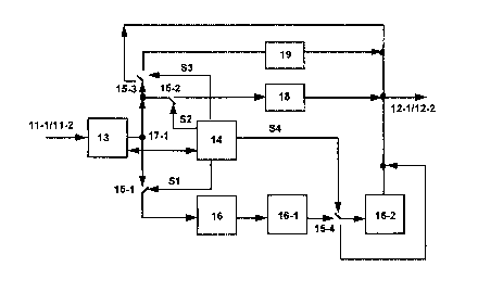
- figure 1 shows a block diagram of a preferred embodiment of an
uninterrupted power supply system according to the invention.
DESCRIPTION OF THE INVENTION
Figure 1 shows a block diagram of the uninterrupted power supply
to system which receives electric power from an electric supply source, such
as
an AC mains line and/or a DC supply unit, through input terminals 11-1 and
11-2, and produces across its output terminals 12-1 and 12-2 a voltage and
current appropriate for a load.
The electric power received through the input terminals 11-1 and
is 11-2, is passed through a filtering means 13 for filtering out the
harmonics
contained in the received current and the electromagnetic interference
conducted over the power lines connected to the terminals 11-1 and 11-2.
The filtered power, before being applied to a determined conversion
path, is examined by a recognising means in order to determine its electrical
2o characteristics and, on a basis of the results of the analysis, to route
the
filtered power to the appropriate conversion path, for completing the power
transformation process and obtaining across the output terminals 12-1 and
12-2 the voltage and current required by the telecommunications equipment.
The uninterrupted power supply system for performing the power
2s transformation process comprises at least a first conversion path, for
example for direct current (DC), and a second conversion path, for example
for alternating current (AC).
The power supply system also comprises a third conversion path able
of storing power and supplying it to the load, in the event of an outage of
the
3o power source.
The third conversion path receives power coming from the output of
the filtering means 13, when a first switching means 15-1 is off, said first
switching means being operated (off and on) by means of a first control
signal S1 generated by the recognising means 14.
3s An end of the first switching means 15-1 is connected, by means of
CA 02293032 1999-12-20
-4-
conductors, to a first node 17-1 located in the output of the filtering means
13; and its other end is connected, by means of conductors, to a charging
device 16.
The power that flows through the first switching means 15-1 is
s adapted for storing in a storage facility 16-1, such as a battery, by means
of
the charging device 16, what is known in the state of the art.
When an outage in the power source arises, the energy stored in the
battery 16-1 before being fed to the load, can be adapted by boosting it in a
first adapting means 16-2, as is a boost switched power converter, for
io example, said boost power converter 16-2 not being described as it is known
in the state of the art.
This connection is made under the control of the recognising means
14, which produces a fourth control signal S4 for activating a fourth
switching
means 15-4, so that the battery 16-1 and the first adapting means 16-2 are
is directly connected to each other. An end of the fourth switching device 15-
4
is connected to the output of the battery 16-1; another of its ends is
connected to the input of the first adapting means 16-2.
In the event of there being no need to adapt the voltage of the battery
16-1, the output of the battery is connected directly to the output terminals
zo 12-1 and 12-2, through another end of the fourth switching means. To this
purpose, the fourth control signal S4 produced by the recognising means 14,
acts on the fourth switching means 15-4 in order to implement said
connection.
The second AC conversion path receives power when a second
Zs switching means 15-2 is turned on, as the electric power source supplies AC
power. The recognising means 14 produces a second control signal S2 for
operating the second switching means 15-2.
An end of the second switching means 15-2 is connected, via a
number of conductors, to the first node 17-1, and its other end is connected,
3o via a number of conductors, to a rectifying means 18, fvr example a diode
bridge, for rectifying the received power, producing at its output a rectified
voltage that is applied directly to the load over the output terminals 12-1
and
12-2.
The first DC conversion path receives power from the first node 17-1
3s when the voltage source provides DC power, this connection being
CA 02293032 1999-12-20
-5-
established by means of a third switching means 15-3, activated by a third
control signal S3 produced by the recognising means 14.
The third switching device 15-3 is connected, via conductors, to the
first node 17-1; another of its ends is connected, via conductors, to a second
s adapting means 19, so that in the event of adapting being required before
supplying to the load, said adapting process is performed by the second
adapting means 19, for example a boost converter. The output of this second
adapter 19 is connected to the output terminals 12-1 and 12-2.
However, when the characteristics of the power supplied by the DC
io source are appropriate for the characteristics required by the load, the
recognising means 14 activates the third switching means 15-3, so that a
direct connection is established between the first node 17-1 and the output
terminals 12-1 and 12-2, which are connected to another end of the third
switching means 15-3.
is As a result, the recognising means 14, by means of the third control
signal S3, activates the third switching means 15-3 so that said connection is
implemented.
The recognising means 14 includes a control logic for analysing the
electrical characteristics of the source and comparing them with the
2o electrical characteristics of the load and, based on the results of the
analysis
pertormed, producing the different control signals S1, S2, S3 and S4 for
setting up the most suitable conversion path for implementing the conversion
process.
The electrical characteristics of the load are inserted into the
2s recognising means 14 during the process of equipping each remote unit, for
example by means of a computer that is connected to a communications port
(not shown) incorporated in the recognising means 14.