Note: Descriptions are shown in the official language in which they were submitted.
CA 02293458 1999-12-10
f
1
SPECIFICATION
IMAGE PROCESSING APPARATUS, AND IMAGE PROCESSING METHOD
TECHNICAL FIELD
The present invention relates to an image processing
apparatus and an image processing method and, more particularly,
to image processing in which input image data is temporarily
stored in storage means, and the stored image data is subjected
to coding.
BACKGROUND ART
Although image data including a time-varying image is
originally analog data, when this data is digitized, various
kinds of complicated signal processing and data compression can
be performed on the data and, therefore, the technology of image
digitization forms an important field. In an image processing
apparatus according to a prior art, input analog image data is
subjected to analog-to-digital conversion and compressive coding
for recording or transmission, and generally the digitized image
data is temporarily stored in a high-speed storage unit such as a
memory before being subjected to compressive coding. An example
of an image processing apparatus with such temporary storage is
disclosed in Japanese Patent Application No. Hei. 7-273461, in
which digital image data is temporarily stored in a memory called
CA 02293458 1999-12-10
2
an image frame memory.
Figure 10 is a block diagram showing the structure of an
image processing apparatus according to the prior art. As shown
in the figure, the prior art image processing apparatus is
provided with an A/D converter 1001, an image input controller
1002, a memory controller 1003, an encoder 1004, an input image
memory 1005, and a rate buffer 1006, and this apparatus receives
an analog video signal S1051 and outputs coded data S1057. In
figure 10, signals shown by solid lines indicate the flow of data
to be processed, and signals shown by broken lines indicate the
flow of signals for control.
The A/D converter 1001 subjects the input analog video
signal S1051 to analog/digital conversion to generate digital
image data 51052. The image input controller 1002 generates an
image input enabling signal 51061 indicating whether the input
digital image data 51052 is "effective" or "ineffective". The
memory controller 1003 controls storage and readout of the
digital image data into/from the memory. The encoder 1004-
subjects the digital image data S1055 to a predetermined
compressive coding process to generate coded data 51056.
The input image memory 1005 temporarily stores the digital
image data S1054 for the work of the compressive coding process.
In the prior art image processing apparatus, the input image
memory is divided into plural regions each region storing a
predetermined quantity of digital image data. Here, the input
CA 02293458 1999-12-10
3
image memory 1005 has two regions, namely, a first region 1005a
and a second region 1005b, each region being able to store one
frame (one screen) of digital image data.
The rate buffer 1006 temporarily stores the coded data
S1056 generated by the coder 1004 and outputs the data so that
the output S1057 from the image processing apparatus is output at
a constant rate. Hereinafter, the operation of the prior art
image processing apparatus so constructed will be described.
When an analog video signal S1051 is input to the image
processing apparatus, the analog video signal S1051 is input to
the A/D converter 1001, wherein it is subjected to analog/digital
conversion. The A/D converter 1001 generates digital image data
S1052 and outputs this data to the image input controller 1002.
The input analog video signal S1051 includes a signal of an
effective region corresponding to a portion of image to be
displayed, and a signal of an ineffective region other than the
effective region. The image input controller 1002 generates an
image input enabling signal S1061 indicating whether the input
digital image data S1052 is "effective" or "ineffective", and
outputs both of the digital image data S1053 and the image input
enabling signal 51061 to the memory controller 1003.
The memory controller 1003 stores the digital image data
S1053 in the input image memory 1005, according to the image
input enabling signal S1061 supplied from the image input
controller 1003 and an image input request signal 1063 supplied
CA 02293458 1999-12-10
4
from the encoder 1004 which is described later. When the encoder
1004 goes into the coding executable state and outputs an image
input request signal S1063 indicating a request for digital image
data to be subjected to coding, to the memory controller 1003,
the memory controller 1003 stores the digital image data 51053 in
the first region 1005a of the input image memory according to the
image input enabling signal 51061 indicating that the digital
image data S1053 is effective.
When a predetermined amount of the digital image data S1053
is stored in the first region 1005a, the memory controller 1003
generates a coding start signal 51062 and outputs it to the
encoder 1004 so that the encoder 1004 starts coding. Here, the
memory controller 1003 generates the signal when one frame of
digital image data has been stored.
The encoder 1004 does not perform coding until it receives
the coding start signal 51062 directing coding, from the memory
controller 1003. When the encoder 1004 has received this signal,
it receives the digital image data S1055 stored in the first
region 1005a through the memory controller 1003, and performs
coding of this data. This coding is carried out according to a
predetermined scheme. For example, one frame of digital image
data is divided into plural blocks each having a predetermined
size, and coding is carried out block by block. When this coding
is carried out, the size of each block is generally 8X8 pixels
or 16x16 pixels. Further, "a pixel" is discrete unit data as a
CA 02293458 1999-12-10
component of digital image data, and it has a pixel value showing
the brightness or color of the image.
The encoder 1004 outputs coded data S1056 generated by the
coding, to the rate buffer 1006. The coded data 51056, which has
temporarily been stored in the rate buffer 1006, is output to the
outside of the image processing apparatus as an output 51057 from
the apparatus, for transmission or the like. On the other hand,
as the coding is executed, the encoder 1004 generates an image
input request signal S1063 indicating that one frame of digital
image data to be coded next is to be input, and outputs this
signal S1063 to the memory controller 1003.
In the memory controller 1003, the digital image data S1053
is stored in the input image memory 1005 according to the image
input request signal S1063 and the input enabling signal 51061
indicating that the digital image data S1053 is effective. As
described above, one frame of digital image data is stored in the
memory 1005. However, at this time, the memory controller 1003
stores the data in the second region 1005b different from the
first region 1005a.
When one frame of digital image data 51053 (a unit of
digital image data) has been stored in the second region 1005b,
the memory controller 1003 generates a coding start signal S1062
indicating that coding should be started, and outputs this signal
to the encoder 1004. If the encoder 1004 has ended coding of the
previous one frame of digital image data (data which were stored
CA 02293458 1999-12-10
6
in the region 1005aj when it receives the coding start signal
S1062 which directs the encoder to start coding, from the memory
controller 1003, the encoder 1004 receives the digital image data
S1055 stored in the second region 1005b through the memory
controller 1003, performs coding of this data, and outputs coded
data to the rate buffer 1006.
As described above, in the prior art image processing
apparatus, digital image data is stored alternately in the first
region 1005a and the second region 1005b possessed by the input
image memory 1005, and the stored data is read alternately from
these regions to be coded by the encoder 1004.
Figure 11 is a timing chart showing the processing status
in the normal state wherein the above-mentioned processing is
carried out normally. In figure 11, "image input request signal
S1063" indicates the state of the signal 51063 output from the
encoder 1004 to the memory controller 1003, and its Hi state
shows that the encoder 1004 requests digital image data. Further,
"image input enabling signal 51061" indicates the state of-the
signal S1061 which is generated by the image input controller
1002 to be output to the memory controller 1003, and its Hi state
shows that the digital image data is effective and to be stored
in the memory.
Furthermore, "image data storage" in figure 11 indicates
regions of the input image memory 1005 where the digital image
data S1054 is stored. As described above, under control of the
CA 02293458 1999-12-10
7
memory controller 1003, the digital image data is stored
alternately in the first region 1005a (in the figure, memory (1))
and the second region 1005b (in the figure, memory (2)), which
regions are possessed by the input image memory 1005.
Turning to figure 11, "coding start signal 51062" indicates
the state of the signal S1062 output from the memory controller
1003 to the encoder 1004, and its Hi state shows that coding
should be started. Further, "coding process" indicates a coding
process performed by the encoder 1004, and it indicates that the
digital image data stored in the first region 1005 (in the figure,
memory (1)) or the second region 1005b (in the figure, memory
(2)) is being subjected to coding, which regions are possessed by
the input image memory 1005.
As shown in the figure, in accordance with the Hi state of
the image input request signal S1063, from timing t110, the
digital image data whose image input enabling signal S1061 is in
the Hi state is stored in the first region, as shown by "image
data storage". Then, in accordance with the Hi state of the
coding start signal S1062 shown in the figure, from timing till,
the digital image data is read from the first region to be coded.
Further, as the coding is carried out, storage of data in the
second region is carried out as shown by "image data storage".
Likewise, from timing t112, storage of data in the first region
and readout of data from the second region are carried out. As
shown by "image data storage" and "coding process" in the figure,
CA 02293458 1999-12-10
8
at the timing when storage of data in one of the regions is
carried out, readout of data from the other region is carried out.
On the other hand, figure 12 is a timing chart showing the
processing state where an error has occurred for some reason, and
this error disables the normal processing shown in figure 11.
Also in this case, the processing is carried out in like manner
as shown in figure 11 until timing t120.
In figure 12, "coding process" indicates that the coding of
the digital image data stored in the second region 1005b (figure
1), which coding has been performed from timing t120, takes time
and, therefore, the end of this coding is delayed to timing t121.
Accordingly, with respect to the second region 1005b of the input
image memory 1005, readout of the digital image data from this
region is carried out until reaching timing t121, and thereby
storage of digital image data into the second region shown by
"image data storage" is not performed although this storage is
ought to be carried out if the processing has been normally
carried out. Therefore, as shown by the broken-line square of
"image data storage" in figure 12, the digital image data which
has not been stored is discarded, i.e., it is not subjected to
the coding process.
After the coding process has ended at timing t122, the
normal processing is carried out again. As described above, in
the prior art image processing apparatus, storage and readout are
alternately performed in/from the regions possessed by the input
CA 02293458 1999-12-10
9
image memory 1005. In this way, the prior art image processing
apparatus is able to perform storage and coding of digital image
data at their respective timings, and copes with a delay or the
like in the coding process by discarding the digital image data.
Also in the apparatus disclosed in the above-mentioned Japanese
Patent Application No. 7-273461, memory management similar to
that mentioned above is performed.
However, the conventional image processing apparatus has
the following problems.
First of all, when the image processing apparatus is used
in a visual telephone system or as a monitor between an input
apparatus such as a video camera and an output apparatus such as
a display, it is required to have the property of operating real-
time. When the apparatus is applied to such use, the apparatus
captures an image from a video camera or the like as a target to
be processed and, after processing, coded data is output from the
apparatus for transmission or the like. At the reproduction end,
the coded data is subjected to decoding and then output as an
image. So, if a delay from inputting analog image data to
displaying output image data is considerable, a time difference
occurs in motions between the real image taken by the camera and
the displayed image, resulting in unnatural image display.
As described above, in the prior art image processing
apparatus, in order to control data input/output to/from the
input image memory, the encoder 1004 starts coding in response to
CA 02293458 1999-12-10
the coding start signal 51062 when the digital image data to be
subjected to coding has been stored by a predetermined amount (in
the above example, one frame) (figure 11). Therefore, in the
prior art image processing apparatus, because of a delay between
the signal input and the start of coding, it is hard to
satisfactorily display the image when the apparatus is applied to
such use. This is the first problem.
Further, in the prior art image processing apparatus, as
described above, unconditional discard of digital image data is
performed for error processing. Since this unconditional discard
causes absence of data, frequent delays in the coding process
result in degradation of image quality. This is the second
problem.
Moreover, since the input image memory 1005 is divided into
the region where storage is performed and the region where
readout is performed, when the amount of digital image data to be
processed is large, the memory capacity must be increased
according to the data amount. However, to require a bulk memory
results in an increase in the cost and, therefore, it is
difficult to fabricate an inexpensive apparatus for propagation.
This is the third problem.
DISCLOSURE OF THE INVENTION
The present invention is made in view of the above-
described circumstances and has an object to provide an image
CA 02293458 2002-12-20
11
processing apparatus which reduces a delay time from start of
signal input to start of coding and, therefore, is suitable for
the real-time use.
Further, the present invention has another object to
provide an image processing apparatus which reduces the amount of
data to be discarded and thereby improves the image quality, even
when a delay or the like occurs during coding.
Further, the present invention has still another object to
provide an image processing apparatus which reduces the capacity
of memory required for temporary storage of digital data and
thereby reduces the cost.
Further, the present invention has yet another object to
provide an image processing method which reduces a delay time
before start of coding, an image processing method which reduces
the possibility of discarding data even if coding is delayed, and
an image processing method which reduces the capacity of memory
required for temporary storage of data.
To attain the above-mentioned objects, one aspect of the present
invention provides an image processing apparatus, which is arL apparatus for
storing input image data in temporary storage means and subjecting the
stored image data to a coding process, comprises: image input control
means for controlling storage of the input image data in the
temporary storage means; storage control means for executing
storage of the image data in the temporary storage means under
control of the image input control means and, when a
CA 02293458 2002-12-20
. 12
predetermined unit storage amount of data has been stored,
generating storage information indicating this; coding means for
reading the image data stored in the temporary storage means to
subject the read data to a predetermined coding process and, when
a predetermined unit processing amount of data has been subjected
to the coding process, generating process information indicating
this; and control information generating means for generating
first control information used by the image input control means
to control the storage, and second control information used by
the coding means to control the coding process; in accordance
with the storage information generated by the storage control
means and the process information generated by the coding means.
Thereby, the control information generating means generates
control information for controlling the storage and the coding
process, according to the image processing status obtained from
the storage information and the process infornvation.
According to an embodiment of the present invention, the
control information generating means generates, as the first
control information, storage stop information indicating that
the storage of the input image data should be stopped, and
generates, as the second control information, cod:Lng stop
information indicating that the coding process should be
stopped. According to the status of image processing, the
storage is stopped to protect the data which have already
been stored, and the coding is stopped to stand by until
CA 02293458 2002-12-20
13
data to be coded are stored.
According to another embodiment of the pre;~ent
invention, the control information generating means
generates, as the first control information, storage stop
information indicating that the storage of the input image data
should be stopped, and generates, as the second control
information, continuous process information indicating how many
times the coding means can continuously perform the coding '
process on the unit processing amount of image data. According
to the status of image processing, the storage is~stopped to
protect the data which have already been stored, and continuous
coding according to the status of storage is performed.
According to another embodiment of the present invention, the
control information generating means comprises: storage information
counting means for counting the storage information and holding
the result as a storage information count value; process
information counting means for counting the process information
and holding the result of the count as a process information
count value; addition control means for outputting an addition
enabling signal when the count of the storage information is
performed by a predetermined number of times, and outputting an
addition disabling signal when the count of the process
information is performed by a predetermined number of times;
storage information count value change means for adding a
CA 02293458 2002-12-20
14
predetermined value to the storage information count value
according to the addition enabling signal or the addition
disabling signal, thereby generating a storage information count
value after processing; codable unit number generating means for
subtracting the process information count value from the storage
information count value after processing, thereby generating a
codable unit number; first control information generating means
for comparing the codable unit number with a first predetermined
value and, when these values match, generating the first control
information; and second control information generating means for
comparing the codable unit number with a second predetermined
value and, when these values match, generating the second control
information. Thereby, the codable unit number indicating the
storage status of data to be coded is obtained from the storage
information and the process information, and the control
information is generated according to the codable unit number to
control the storage and the coding.
According to another embodiment of the present invention, the
control information generating means comprises: storage information
counting means for counting the storage information and holding
the result as a storage information count value; process.
information counting means for counting the process information
and holding the result as a process information count value;
addition control means for outputting an addition enabling signal
CA 02293458 2002-12-20
when the count of the storage information has been performed by a
predetermined number of times, and outputting an addition
disabling signal when the count of the process information has
been performed by a predetermined number of times; storage
information count value change means for adding a predetermined
value to the storage information count value according to the
addition enabling signa-1 or the addition disabling aignal,
thereby generating a storage information count value after
processing; codable unit number generating means for subtracting
the process information count value from the storage information
count value after processing, thereby generating a codable unit
number; and first control information generating means for
comparing the codable unit number with a first predetermined
value and, when these values match, generating the first control
information; wherein the codable unit number :i.s usedl as the
second control information. Thereby, the cod~ble unit number
indicating the storage status of data to be coded is obtained
from the storage information and the process information, and the
control information is generated according to the codable unit
number to control the storage and the continuous coding.
Another aspect of the present invention provides an image processing
method, which is a method for storing input image data in temporary
storage means and performing coding of the stored image data, comprises:
image input control step of controlling storage of the input: image data
in the temporary storage means; storage control step of executing
CA 02293458 2002-12-20
s
storage of the image data in the temporary storage means under
control of the image input control step and, when a predetermined
unit storage amount of data has been stored, generating storage
information indicating this; coding step of reading the image
data stored in the temporary storage means to subject the read
data to a predetermined coding process and, when a predetermined
unit processing amount of data has been subjected to the coding
process, generating process information indicating this; and
control information generating step of generating first control
information used in the image input control step to control the
storage, and second control information used in the coding step
to control the coding process, according to the storage
information generated in the storage control step and the process
information generated in the coding step. Thereby, in the
control information generating step, the control information for
controlling the storage and the coding process is generated
according to the image processing status obtained from the
storage information and the process information.
According to another embodiment of the present
invention, in the control information generating step,
storage stop information indicating that the storage of the
input image data should be stopped is generated as the first
control information, and coding stop information indicating
that the coding process should be stopped is generated as the
second control information. According to the status of
CA 02293458 2002-12-20
1~
image processing, the storage is stopped to protect the data
which have already been stored, and the coding is stopped to
stand by until data to be coded are stored.
According to another embodiment of the present
invention, in the control information generating step,
storage stop information indicating that the storage of
the input image data should be stopped is generated as
the first control information, and continuous process information
indicating how many times the coding process on the unit
processing amount of image data can be continuously performed in
the coding step is generated as the second control information.
According to the status of image processing, the storage is
stopped to protect the data which have already been stored, and
continuous coding according to the status of storage is performed.
According to another embodiment of the present
invention, the control information generating step
comprises: storage information counting step of counting
the storage information and holding the result as a storage
information count value; process information counting step
of counting the process info-rmation and holding the result
as a process information count value; addition control step of
outputting an addition enabling signal when the count of the
storage information is performed by a predetermined number of
times, and outputting an addition disabling signal when the count
of the process information is performed by a predetermined number
CA 02293458 2002-12-20
1 8
of times; storage information count value change step of adding a
predetermined value to the storage information count value
according to the addition enabling signal or the addition
disabling signal, thereby generating a storage information count
value after processing; codable unit number generating step of
subtracting the process information count value from the storage
information count value after processing, thereby generating a
codable unit number; first control information generating step of
comparing the codable unit number with a first predetermined
value and, when these values match, generating the first control
information; and second control information generating step of
comparing the codable unit number with a second predetermined
value and, when these values match, generating the second control
information. Thereby, the codable unit number indicating the
storage status of data to be coded is obtained from the_storage
information and the process information, and the control
information is generated according to the codable unit number to
control the storage and the coding.
According to another embodiment of the present
invention, the control information generating step comprises:
storage information counting step of counting the storage
information and holding the result as a storage information
count value; process information counting step of counting
the process information and holding the result as a process
information count value; addition control step of
CA 02293458 1999-12-10
19
outputting an addition enabling signal when the count of the
storage information is performed by a predetermined number of
times, and outputting an addition disabling signal when the count
of the process information is performed by a predetermined number
of times; storage information count value change step of adding a
predetermined value to the storage information count value
according to the addition enabling signal or the addition
disabling signal, thereby generating a storage information count
value after processing; codable unit number generating step of
subtracting the process information count value from the storage
information count value after processing, thereby generating a
codable unit number; first control information generating step of
comparing the codable unit number with a first predeterntined
value and, when these values match, generating the first control
information; and second control information generating step in
which the codable unit number is used as the second control
information. Thereby, the codable unit number indicating the
storage status of data to be coded is obtained from the storage
information and the process information, and the control
information is generated according to the codable unit number to
control the storage and the continuous coding.
BRIEF DESCRIPTION OF THE DRAWINGS
Figure 1 is a block diagram illustrating the structure of
an image processing apparatus according to a first embodiment of
CA 02293458 1999-12-10
the present invention.
Figure 2 is a block diagram illustrating the internal
structure of a flag generator included in the image processing
apparatus according to the first embodiment.
Figures 3(a)-3(c) are diagrams for explaining the structure
of digital image data to be processed by the image processing
apparatus according to the first embodiment.
Figures 4 and 5 are timing charts for explaining the
processing by the image processing apparatus according to the
first embodiment.
Figure 6 is a block diagram illustrating the structure of
an image processing apparatus according to a second embodiment of
the present invention.
Figure 7 is a block diagram illustrating the internal
structure of a flag generator included in the image processing
apparatus according to the second embodiment.
Figures 8 and 9 are timing charts for explaining the
processing by the image processing apparatus according to the
second embodiment.
Figure 10 is a block diagram illustrating the structure of
an image processing apparatus according to the prior art.
Figures 11 and 12 are timing charts for explaining the
processing by the image processing apparatus according to the
prior art.
CA 02293458 1999-12-10
21
BEST MODE TO EXECUTE THE INVENTION
Embodiment 1
An image processing apparatus according to a first
embodiment of the present invention is provided with a flag
generator, and controls image processing and manages a memory by
using control flags.
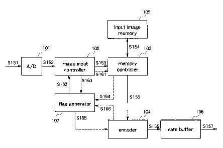
Figure 1 is a block diagram illustrating the structure of
the image processing apparatus according to the first embodiment,
which receives analog image data and subjects the data to digital
conversion and compressive coding. As shown in the figure, the
image processing apparatus according to the first embodiment is
provided with an A/D converter 101, an image input controller 102,
a memory controller 103, an encoder 104, an input image memory
105, a rate buffer 106, and a flag generator 107. This apparatus
receives an analog video signal 5151, and outputs coded data S157.
In figure 1, signals shown by solid lines indicate the flow of
data to be processed, and signals shown by broken lines indicate
the flow of signals for control.
The A/D converter 101 subjects the input analog video
signal 5151 to analog/digital conversion to generate digital
image data S152. The image input controller 102 generates an
image input enabling signal 5161 indicating whether the input
digital image data S152 is "effective" or "ineffective". In this
first embodiment, as in the case of the prior art image
processing apparatus, the image input controller 102 generates an
CA 02293458 1999-12-10
22
image input enabling signal S161 according to the distinction
between the effective region and the ineffective region of the
digital image data and, further, it refers to an error flag S162
supplied from the flag generator 107 which will be described
later. When the error flag S162 is ineffective (Lo state), the
image input controller 102 generates an image input enabling
signal S161 indicating "effective". When the error flag 5162 is
effective (Hi state), it generates an image input enabling signal
S161 indicating "ineffective".
The memory controller 103 controls storage and readout of
digital image data in/from the memory. The memory controller 103
according to this first embodiment controls storage and readout
of digital image data in/from the input image memory 105 for a
predetermined amount as a unit and, when storage of data for each
unit has been completed, it generates a writing end signal S164
indicating the completion and then outputs this signal to the
flag generator 107. Therefore, the memory controller 103
functions as a storage control means which performs storage of
digital image data into a temporary storage means (input image
memory 105) under control of an image input control means (image
input controller 102) and generates storage information (writing
end signal 5164) when a predetermined amount (unit amount) of
data has been stored.
The encoder 104 subjects the digital image data S155 to a
predetermined compressive coding process to generate coded data
CA 02293458 1999-12-10
23
5156. The encoder 104 according to this first embodiment refers
to an empty flag S165 which is supplied from the flag generator
107 described later. When the empty flag S165 is in the Lo state,
the encoder 104 performs coding, and when the empty flag S165 is
in the Hi state, the encoder 104 does not perform coding.
Further, the encoder 104 performs coding for a predetermined
amount of data as a unit. When coding for each unit has been
completed, it generates a coding end signal S166 indicating the
completion and outputs this signal to the flag generator 107.
Accordingly, the encoder 104 functions as a coding means which
reads image data stored in a temporary storage means (input image
memory 105), subjects the data to a prescribed coding process,
and generates process information (coding end signal S166) when a
predetermined amount (unit amount) of data has been coded.
The input image memory 105 temporarily stores the digital
image data S154 for the work of compressive coding. In this
first embodiment, in contrast with the prior art image processing
apparatus, the memory 105 is not divided into specific regions
(two regions in the prior art example) to be managed, and a
capacity enough to store a predetermined amount (one frame) of
digital image data suffices for the input image memory 105. The
rate buffer 106 temporarily stores the coded data 5156 so that
the coded data S157, which is output from the image processing
apparatus, is output at a constant rate.
The flag generator 107 counts the writing end signal for
CA 02293458 1999-12-10
24
each unit amount supplied from the memory controller 103 and the
coding end signal for each unit amount supplied from the encoder
104 and, according to the result of the count, it generates flags
(empty flag and error flag) used for controlling input/output of
the data to/from the memory. Therefore, the flag generator 107
functions as a control information generating means which
generates first control information (error flag) used by an image
input control means (image input controller 102) to control
storage, and second control information (empty flag) used by a
coding means (encoder 104) to control coding, according to the
storage information (writing end signal S164) generated by the
storage control means (memory controller 103) and the process
information (coding end signal S166) generated by the coding
means (encoder 104).
Figure 2 is a block diagram illustrating the internal
structure of the flag generator 107 (figure 1). As shown in
figure 2, the flag generator 107 is provided with a write block
counter 201, a read block counter 202, a carry flag holder 203, a
selector 204, an adder 205, a subtracter 206, first and second
comparators 207 and 208, an error flag holder 209, and an empty
flag holder 210.
The write block counter 201 counts the writing end signal
5164 supplied from the memory controller 103 (figure 1) for each
slice (described later) as a unit, and outputs the count value to
the adder 205 while holding it. This count is carried out
CA 02293458 1999-12-10
according to tetradecimal number system. When the count value
has reached 14 and the next writing end signal S164 has been
input, the count value becomes 0 and the carry flag holder 203
(described later) enters in the set state. Further, when a
counter reset signal S163a instructing initialization is supplied
from the image input controller 102 (figure 1), the count value
becomes 0. Accordingly, the write block counter 201 functions as
a storage information count means which counts the storage
information (writing end signal S164) and holds the result of the
count as a storage information count value.
The read block counter 202 counts the coding end signal
S166 supplied from the encoder 104 (figure 1) for each slice
(described later) as a unit, and outputs the count value to the
adder 206 while holding it. This count is carried out according
to tetradecimal number system. When the count value has reached
14 and the next coding end signal S166 has been input, the count
value becomes 0 and the carry flag holder 203 described later
enters in the reset state. Accordingly, the read block counter
202 functions as a process information count means which counts
the process information (coding end signal 5166) and holds the
result of the count as a process information count value.
The carry flag holder 203 is set when the counting
operation of the write block counter 201 has reached 15, namely,
when the count value of the write block counter has reached 14
and become 0 by the input of the next writing end signal, and the
CA 02293458 1999-12-10
26
carry flag holder 203 is reset when the read block counter 202
counts 15, namely, when the count value of the read block counter
has reached 14 and become 0 by the input of the next coding end
signal. The carry flag holder 203 outputs a signal S253 to the
selector 204, which signal 5253 is in the Hi state when the
holder 203 is in the set state and in the Lo state when the
holder 203 is in the reset state.
When the selector 204 is supplied with the value 0 (signal
S254a) and the value 15 (signal S254b), it selects one of these
values according to the signal 5253 supplied from the carry flag
holder 203, and outputs the selected value to the adder 205. The
selector 204 selects 0 when the signal 5253 is in the Lo state
while it selects 15 when the signal S253 is in the Hi state.
The adder 205 adds the count value (signal S251) of the
write block counter 201 and the value (signal 5255) output from
the selector 204, and outputs the result (signal S256) to the
subtracter 206. The subtracter 206 subtracts the count value
(signal S252) of the read block counter 202 from the sum (signal
5256) output from the adder 205. The subtracter 206 outputs a
signal 5257 indicating the result obtained by the subtraction to
the first and second comparators 206 and 207. Accordingly, the
carry flag holder 203, the selector 204, and the adder 205
function as an addition control means which outputs an addition
enabling signal when the count of the storage information
(writing end signal 5164) is carried out by a predetermined
CA 02293458 1999-12-10
2?
number of times, and outputs an addition disabling signal when
the count of the process information (coding end signal S165) is
carried out by a predetermined number of times, and as a storage
information count value change means which adds a predetermined
value (signal S255) to the storage information count value (count
value of the write block counter 201) according to the addition
enabling signal or the addition disabling signal to generate a
storage information count value after processing (signal S256).
Further, the subtracter 206 functions as a codable unit number
generating means which subtracts the process information count
value (signal 5252) from the storage information count value
after processing (signal S256) to generate a codable unit number
(signal S257).
The first and second comparators 207 and 208 receive a
signal S258a indicating l5and a signal S258b indicating 0 ,
respectively. The comparator 207 compares the signal S258a with
the signal S257 while the comparator 208 compares the signal
S258b with the signal S257 to decide whether these signals match
each other or not. According to the result of the comparison,
the comparator 207 generates a signal 5259 indicating whether the
signal S258a matches the signal S257 or not, and outputs it to
the error flag holder 209. According to the result of the
comparison, the comparator 208 generates a signal 5260 indicating
whether the signal S258b matches the signal S257 or not, and
outputs it to the empty flag holder 210.
CA 02293458 1999-12-10
28
The error flag holder 209 is set when the signal S259
supplied from the comparator 20~ indicates "match", namely, when
the signal S257 is 15, and it is reset when an error reset signal
S163b output from the image input controller 102 (figure 1) is
input thereto. The error flag holder 209 outputs an error flag
S162 in the Hi state when it is in the set state while it outputs
an error flag S162 in the Lo state when it is in the reset state,
to the image input controller 102 (figure 1).
The empty flag holder 210 generates an empty flag S165 in
the Hi state when the signal 5260 supplied from the comparator
208 indicates "match", that is, when the signal S257 is 0. The
empty flag 5165 is output to the encoder 104 as shown in figure 1.
Accordingly, the first comparator 207 and the error flag
holder 209 function as a first control information generating
means which compares the codable unit number (signal 5257) with a
first prescribed value (signal S258a), and generates the first
control information (error flag S162 in the Hi state) when these
signals match. Further, the second comparator 208 and the empty
flag holder 210 function as a second control information
generating means which compares the codable unit number (signal
S257) with a second prescribed value (signal S258b), and
generates the second control information (empty flag 5165 in the
Hi state) when these signals match. Further, the error flag S162
in the Hi state is used as storage stop information indicating
that storage of the input image data should be stopped, and the
CA 02293458 1999-12-10
29
empty flag S165 in the Hi state is used as coding stop
information indicating that coding should be stopped.
Figure 3 is a diagram showing an example of a format of
digital image data in the image processing apparatus according to
the first embodiment. The digital image data output from the A/D
converter 101 possessed by the image processing apparatus
according to this first embodiment is discrete unit digital data,
and it is an array of pixels having pixel values each showing a
luminance signal or a color difference signal of an image. As
shown in figure 3(a), one frame comprises 352X240 pixels.
Figure 3(b) shows coded blocks, each coded block being a
processing unit of coding by the encoder 104 and comprising 16X
16 pixels. As shown in the figure, one frame of digital image
data comprises 22 coded blocks in the horizontal direction and 15
coded blocks in the vertical direction. Figure 3(c) shows slices,
each slice being an input/output unit of digital image data
according to this first embodiment. One slice is one array of
coded blocks in the horizontal direction. As shown in the figure,
one slice comprises 22 coded blocks in the horizontal direction
and 1 coded block in the vertical direction, and one frame
comprises 15 slices.
In this first embodiment, input/output of digital image
data in/from the input image memory 105 is managed in units of
slices. Therefore, each of the unit storage amount and the unit
processing amount is one slice.
CA 02293458 1999-12-10
Hereinafter, a description will be given of the operation
of the image processing apparatus according to the first
embodiment constructed as shown in figures 1 and 2. In the
initial state, since system reset is performed, the count values
of the write block counter 201 (figure 2) and the read block
counter 202 (figure 2) possessed by the flag generator 107
(figure 1) become 0, and the carry flag holder 203 (figure 2) and
the error flag holder 209 (figure 2) are in their reset states.
Accordingly, the error flag 5162 output from the flag generator
107 shown in figure 1 is in the ineffective state, namely, the Lo
state.
In the initial state, the flag generator 107 shown in
figure 2 operates as follows. The signal S251 indicating 0 is
output from the write block counter 201 to the adder 205. In
this case, since the carry flag holder 203 is in the reset state,
the signal S253 is in the Lo state, 0 is selected in the selector
204, and the signal S255 indicating 0 is output to the adder 205.
In the adder 205, the signal 5251 (0) and the signal 5255 (0) are
added, and the signal S256 indicating 0 which is the result of
the addition is output to the subtracter 206. On the other hand,
from the read block counter, the signal S252 indicating the count
value 0 is output to the subtracter 206. The subtracter 206
subtracts the signal S252 (0) from the signal 5256 (0), and
outputs the signal S257 indicating 0 which is the result of the
subtraction, to the comparators 207 and 208.
CA 02293458 1999-12-10
31
The comparator 207 compares the signal S257 (0) with the
signal S258a indicating the constant 15. Since these signals do
not match, the comparator 207 does not perform the setting
operation for the error flag holder 209. Therefore, the error
flag holder 209 remains in the reset state, and the output error
flag 5162 remains in the Lo state.
On the other hand, in the comparator 208, the signal 5257
(0) is compared with the signal S258b indicating the constant 0.
Since these signals match, the comparator 208 outputs the signal
S260 indicating "match" to the empty flag holder 210. Thereby,
the empty flag holder 210 outputs the empty flag S165 in the Hi
state.
The empty flag 5165 in the Hi state means that digital
image data to be coded is not stored in the input image memory
105. The empty flag S165 is input to the encoder 104 as shown in
figure 1, and the encoder 104 does not perform coding when the
empty flag S165 is in the Hi state. Accordingly, the encoder 104
is in the stand-by state until a prescribed amount of data is
stored in the input image memory 105.
As shown in figure 1, when the analog video signal 5151 is
input to the image processing apparatus, the analog video signal
5151 is input to the A/D converter 101 and subjected to
analog/digital conversion. The A/D converter 101 outputs the
digital image data S152 so generated to the image input
controller 102. The image input controller 102 reads the error
CA 02293458 1999-12-10
32
flag S162 supplied from the flag generator 107. As described
above, since the error flag S162 is in the ineffective state (Lo
state), the image input controller 102 generates an image input
enabling signal S161 corresponding to the input digital image
data S152 as a signal indicating "effective" (Hi state), and
outputs the digital image data S153 and the image input enabling
signal 5161 to the memory controller 103.
Since the image input enabling signal S161 indicates
"effective", the memory controller 103 stores the corresponding
digital image data 5152 in the input image memory 105. As
already described with respect to figure 3, input/output of the
digital image data in/from the input image memory is carried out
in slice units (figure 3(c)). So, when the memory controller 103
has stored one slice of digital image data in the input image
memory, it generates a writing end signal S164 to be output to
the flag controller 107.
In the flag generator 107, the writing end signal S164 is
input to the write block counter 201 as shown in figure 2, and
the write block counter performs the count-up operation to
increase its count value by 1. In the figure, since the count
value of the write block counter 201 changes from 0 to 1, the
signal S251 indicating 1 is output from the write block counter
201 to the adder 205. Since the carry flag holder 203 remains in
the reset state, 0 is selected in the selector 204 according to
the signal 5253 indicating the reset state, and the signal S255
CA 02293458 1999-12-10
33
indicating 0 is output to the adder 205. In the adder 205, the
signal S251 (1) and the signal S255 (0) are added, and the signal
S256 indicating 1, which is the result of the addition, is output
to the subtracter 206. On the other hand, the count value of the
read block counter is 0, and so the signal S252 indicating 0 is
output to the subtracter 206. The subtracter 206 subtracts the
signal S252 (0) from the signal 5256 (1), and outputs the signal
5257 indicating 1, which is the result of the subtraction, to the
comparators 207 and 208.
The comparator 207 compares the signal 5257 (1) with the
signal S258a indicating the constant 15. Since these signals do
not match, the comparator 207 does not perform the setting
operation for the error flag holder 209. Accordingly, the error
flag holder 209 remains in the reset state, and the output error
flag S162 remains in the Lo state.
On the other hand, the comparator 208 compares the signal
5257 (1) with the signal S258b indicating the constant 0. Since
these signals do not match, the comparator 208 outputs the signal
S260 indicating "mismatch" to the empty flag holder 210. Thereby,
the empty flag holder 210 outputs the empty flag 5165 in the Lo
state.
Turning to figure 1, the empty flag 5165 in the Lo state is
input to the encoder 104. Since the empty flag S165 in the Lo
state indicates that digital image data to be subjected to coding
is stored in the input image memory 105, the encoder 104 executes
CA 02293458 1999-12-10
34
coding when detecting this flag. The digital image data stored
in the input image memory 105 is read by the encoder 104 through
the memory controller 103. The encoder 104 codes the input
digital image data S155 to generate coded data S156, and outputs
the data to the rate buffer 106. From the rate buffer 106, the
coded data 5157 is output at a constant rate to the outside of
the image processing apparatus.
On the other hand, when coding of the one slice of digital
image data has been completed, the encoder 104 generates a coding
end signal S166 indicating the completion, and outputs this
signal to the flag generator 107. In the flag generator 107, the
coding end signal 5166 is input to the read block counter 202 as
shown in figure 2, and the read block counter 202 performs the
count-up operation to increase its count value by 1.
Thereafter, the image input controller 102 checks the state
of the error flag 5162, and the digital image data is
continuously stored in the input image memory 105 as long as the
error flag is in the Lo state. On the other hand, the encoder
104 checks the state of the empty flag S165 every time one slice
of digital image data is coded. When the empty flag is in the Lo
state, the encoder 104 reads the digital image data stored in the
input image memory 105 and codes the data.
In the flag generator 107, the write block counter 201
shown in figure 2 performs the count-up operation every time the
writing end signal S164 output from the memory controller 103
CA 02293458 1999-12-10
(figure 1) is input thereto. When the count value has reached 14
and a further writing end signal S164 has been input, the write
block counter 201 instructs the carry flag holder 203 to be in
the set state, and sets its own count value to 0. In other words,
the carry flag holder 203 goes into the set state when the count
value of the write block counter 201 becomes 15 which is equal to
the number of slices constituting one frame (figure 3(c)).
The read block counter 202 shown in figure 2 performs the
count-up operation every time the coding end signal S166 output
from the encoder 104 (figure 1) is input thereto. When the count
value has reached 14 and a further coding end signal S166 has
been input, the read block counter 202 instructs the carry flag
holder 203 to be in the reset state, and sets its own count value
to 0. In other words, the carry flag holder 203 goes into the
reset state when the count value of the read block counter 202
becomes 15 which is equal to the number of slices constituting
one frame (figure 3(c)).
When the carry flag holder 203 is in the set state, as the
signal S253 is in the Hi state, the selector 204 selects the
signal S254b indicating 15 and outputs the signal S255 indicating
15 to the adder 205. In this case, in the adder 205, 15 is added
to the count value of the write block counter 201, and the result
of the addition S256 is output to the subtracter 206.
The result obtained in the subtracter 206 is a difference
between "the number of slices stored in the input image memory
CA 02293458 1999-12-10
36
105" (S251=S256) and "the number of slices coded by the encoder
104" (S252) when the carry flag holder 203 is in the reset state.
On the other hand, when the carry flag holder 203 is in the set
state, the result is a difference between "the number of slices
stored in the input image memory 105 + 15" (5251+15=S256) and
"the number of slices coded by the encoder 104" (5252). When
this difference is 0, the empty flag S165 is in the Hi state, and
the coding by the encoder 104 is stopped. When the difference is
15, the error flag S162 is in the Hi state, and the image input
controller 102 generates an image input enabling signal 5161
indicating "ineffective", and therefore storage of digital image
data in the input image memory is not carried out.
Figures 4 and 5 are timing charts showing examples of
processing states of the image processing apparatus according to
the first embodiment. In figures 4 and 5, "image input enabling
signal S161" is a signal generated by the image input controller
102 to be output to the memory controller 103 in figure 1, and
its Hi state indicates "effective" and instructs storage of
digital image data in the input image memory while its Lo state
indicates "ineffective" and does not instruct storage of digital
image data in the input image memory 105. "Digital image data
5153" indicates digital image data in slice units to be output to
the memory controller 103 together with the image input enabling
signal 5161.
In figures 4 and 5, "write block counter 201" indicates the
CA 02293458 1999-12-10
37
count value possessed by the write block counter 201 in figure 2.
The write block counter 201 counts the writing end signal S164
which is output from the memory controller 103 shown in figure 1
and indicates that storage of digital image data for each slice
has been performed, and the count value corresponds to the number
of slices of digital image data stored in the input image memory
105.
In figures 4 and 5, "carry flag (S253)" indicates the state
of the signal S253 indicating whether the carry flag holder 203
is in the set state or in the reset state, in figure 2. As
described above, the signal S253 is in the Hi state when the
holder 203 is in the set state while it is in the Lo state when
the holder 203 is in the reset state, and this signal controls
the selection of the selector 204.
In figures 4 and 5, "empty flag S165" indicates the state
of a signal which is generated by the flag generator 107 and
output to the encoder 104 in figure 1, and its Hi state indicates
that no digital image data to be coded is stored in the input
image memory 105, and instructs the encoder 104 to stop coding.
Its Lo state indicates that digital image data to be coded is
stored in the input image memory 105, and instructs the encoder
104 to execute coding.
In figures 4 and 5, "error flag S162" indicates the state
of a signal which is generated by the flag generator 107 and
output to the image input controller 102 in figure 1, and its Hi
CA 02293458 1999-12-10
38
state indicates overflow in the input image memory 105, and
instructs the image input controller 102 to generate an image
input enabling signal indicating "ineffective" (to stop storage
of data in the input image memory 105). Its Lo state indicates
that storage of data in the input image memory 105 is possible,
and instructs the image input controller 102 to generate an image
input enabling signal indicating "effective" (to execute storage
of data in the input image memory 105).
In figures 4 and 5, "read block counter 202" indicates the
count value held by the read block counter 202, in figure 2. The
read block counter 202 counts the coding end signal 5166 which is
output from the encoder 104 shown in figure 1 and indicates that
coding for each slice has been performed, and the count value
corresponds to the number of slices of digital image data which
have been coded.
In figures 4 and 5, "coding process (104)" indicates the
coding process in slice units performed by the encoder 104. The
time required for coding of digital image data significantly
varies according to the characteristics of the image and,
therefore, there are both cases where the time required for
processing one slice is long and where it is short, as shown in
figures 4 and 5.
Hereinafter, the image processing by the image processing
apparatus according to the first embodiment will be described
along the timing chart of figure 4.
CA 02293458 1999-12-10
39
Since no effective region of the image is input until
timing t40 shown in figure 4, the image input controller 102
outputs the image input enabling signal S161 in the Lo state, and
storage of digital image data is not carried out. From timing
t40, the first frame of digital image data S153 is input to be
processed. Since the error flag S162 is in the Lo state in the
initial state, the image input controller 102 generates an image
input enabling signal S161 in the Hi state indicating "effective",
so that the digital image data S153 is stored in the input image
memory 105.
Every time one slice of data is stored, the memory
controller 103 outputs a writing end signal S164 to the flag
generator 107, and the write block counter 201 possessed by the
flag generator 107 performs the count-up operation corresponding
to the signal S164. Here, every time the slices constituting the
digital image data of the first frame (15 slices from 0 to 14)
are input, the count value increases to 14.
At timing t41 when one slice of the digital image data S153
has been stored, the count value of the write block counter 201
changes from 0 to 1 as described above, whereby the empty flag
changes from the Hi state to the Lo state. Accordingly, the
encoder 104, detecting that the empty flag is in the Lo state,
reads the digital image data stored in the input image memory 105
to code the data. Every time coding of one slice has ended, a
coding end signal S166 is output, and the read block counter 202
CA 02293458 1999-12-10
possessed by the flag generator 107 performs the count-up
operation corresponding to the signal S166.
Between timing t41 and timing t42, coding is carried out
speedily and, immediately after t42, the input image memory 105
enters in the state where the digital image data to be subjected
to coding has not yet been completely stored therein. In this
case, since the value of the signal S257 output from the
subtracter 206 shown in figure 2 becomes 0, the empty flag in the
Hi state is output according to the result of the comparison in
the comparator 208. Therefore, as shown in figure 4, the encoder
104 stops coding. Here, when the next slice is stored in the
input image memory 105, the empty flag S165 returns to the Lo
state, and coding is resumed.
Until timing t43, the first frame of digital image data
S153 has been stored in the input image memory 105. At this time,
since the write block counter 201 receives the writing end signal
S164 while it holds the count value 14, the counter 201 instructs
the carry flag holder 203 shown in figure 2 to be in the set
state and sets its own count value to 0. Thereby, the signal
5253 output from the carry flag holder 203 goes into the Hi state,
and in the adder 205, 15 is added to the count value of the write
block counter 201.
At timing t44, the second frame of digital image data S153
is input. Since the error flag S162 remains in the Lo state, the
image input controller 102 outputs the image input enabling
CA 02293458 1999-12-10
41
signal S161 indicating "effective", whereby the first slice of
the input digital image data is stored so that it overwrites the
already coded slice of digital image data in the first frame,
under control of the memory controller 103. The subsequent
slices of the digital image data 5153 are also stored in the
input image memory 105 so that these slices overwrite the already
coded slices. Thereafter, at timing t45, the encoder 104
completes coding of the digital image data in the first frame.
The read block counter 202 (count value 14) receiving the coding
end signal S166 at this time resets the carry flag holder 203
shown in figure 2 and sets its own count value to 0. Therefore,
the signal S253 shown in figure 4 goes into the Lo state, and in
the adder 205 the value to be added to the write block counter
201 is changed from 15 to 0.
As described above, in the image processing apparatus of
the first embodiment, even when the input image memory 105 having
a capacity for one frame comes into the state where one frame of
data has already been stored, the subsequent one frame of data is
processed so that it overwrites in slice units, in contrast with
the prior art image processing apparatus in which one frame of
data is immediately discarded. To be specific, in the prior art
image processing apparatus, the second frame of digital image
data shown in figure 4 is discarded without being coded. However,
in the image processing apparatus according to the first
embodiment, the second frame o.f data is not discarded but coded
CA 02293458 1999-12-10
42
according to the above-mentioned processing.
However, also in the image processing apparatus of this
first embodiment, there is a case where digital image data is
discarded according to control using an error flag. Figure 5 is
a diagram for explaining processing in this case.
In figure 5, from timing t50, the i-th frame of digital
image data S153 is stored in the input image memory 105 and,
thereafter, the encoder 104 starts coding. At timing t51,
storage of the i-th frame of digital image data S153 is completed.
As in the case shown in figure 4, the signal S253 output from the
carry flag holder 203 goes into the Hi state and, from timing t52,
the (i+1)th frame of digital image data is stored so that it
overwrites the already coded data. At timing t53, the 11th slice
of data in the (i+1)th frame is to be stored, but coding of the
11th slice of data in the i-th frame has not yet been completed
at this point of time.
In such case, in figure 2, the count value 11 of the write
block counter and the value 15 output from the selector 204 are
added by the adder 205, and the value 26 (signal S256) is output
to the subtracter 206. On the other hand, the count value of the
read block counter 202 becomes 11, and the signal S252 indicating
11 is output to the subtracter 206. The result obtained by the
subtracter 206 becomes 26-11=15, and the signal 5257 having the
value 15 is output to the comparator 207, whereby the error flag
S162 goes into the Hi state. Since the error flag S162 is Hi as
CA 02293458 1999-12-10
43
shown in figure 5, the image input controller 102 sets the image
input enabling signal S161 in the Lo state indicating
"ineffective". So, the digital image data is discarded without
being stored in the input image memory 105. Accordingly, the
11th and subsequent slices of digital image data in the i-th
frame, for which coding has not completed yet, are stored without
being overwritten.
At timing t54, the image input controller 102 outputs the
counter reset signal 5163 to the flag generator 107. The write
block counter 201 shown in figure 2 sets the count value to 0 in
response to the signal S163a. The number of slices of digital
image data stored in the input image memory 105 indicates the
number of remaining slices which have not yet been coded, amongst
the slices constituting the i-th frame of digital image data.
Timing t55 is the timing at which storage of the (i+1)th
frame of digital image data ought to be completed if the
processing has been carried out normally. At this point of time,
the image input controller 102 shown in figure 1 outputs the
error reset signal S163 to the flag generator 107. As shown in
figure 2, the error reset signal S163b is input to the error flag
holder 209, whereby the state of the error flag holder 109 is
changed from the set state to the reset state. Accordingly, the
error flag output from the flag generator 107 changes from the Hi
state to the Lo state.
Further, at timing t56, the read block counter 202 holding
CA 02293458 1999-12-10
44
the count value 14 receives the coding end signal 5166, and it
changes the state of the carry flag holder 203 to the reset state
and sets its own count value to 0. Accordingly, the signal S253
output from the carry flag holder 203 changes from the Hi state
to the Lo state, and 0 is added in the adder 205 shown in figure
2. Accordingly, both of the signal S256 and the signal S252
become 0 and the signal S257 becomes 0, whereby the empty flag
S165 in the Hi state is output.
In response to this, the encoder 104 stops coding and, as
shown in figure 5, the coding stop period continues until the
subsequent data is stored.
At timing t57, the (i+2)th frame of digital image data S153
is stored in the input image memory 105. Thereby, in figure 2,
the count value of the write block counter 201 changes from 0 to
1, and the value of the signal S257 changes from 0 to l, whereby
the empty flag S165 in the Lo state is output. Accordingly, as
shown in figure 5, on and after timing t57 when the empty flag
S165 goes in the Lo state, coding by the encoder 104 is resumed
to process the (i+2)th frame of data.
In the image processing apparatus according to the first
embodiment, since the overwrite storage in slice units is carried
out as shown in figure 4, the second frame of digital image data
is not discarded even when coding is delayed. However, as shown
in figure 5, when the delay increases and the overwrite storage
in slice units adversely affects the unprocessed data in the i-th
CA 02293458 1999-12-10
frame, the (i+1)th frame of data is not subjected to coding in
the above-described processing to protect the i-th frame of data,
and subsequently the (i+2)th frame of data is subjected to coding.
As described above, since the image processing apparatus
according to the first embodiment is provided with the flag
generator 107 which holds a carry flag in it and generates an
error flag and an empty flag, the encoder 104 starts coding in
accordance with the state of the empty flag. Therefore, the
coding can be started when one slice of digital image data has
been stored in the input image memory 105, whereby a delay until
starting the coding can be reduced as compared with the prior art
image processing apparatus which requires storage of data in one
frame (in the image format shown in figure 3, 15 slices),
resulting in an image processing apparatus suitable for the real-
time use.
A description is now given of comparison of delays between
the image processing apparatus according to the first embodiment
and the image processing apparatus according to the prior art.
According to general conditions, it is assumed that the target to
be processed is according to the NTSC (1 line = about 63.5us)
system, the image size to be stored in the input image memory is
352 pixels X 240 pixels (352 pixels X 240 lines) for one frame,
and the slice size (the processing unit of the first embodiment)
is 352 pixels X 16 pixels (352 pixels X 16 lines) for one slice.
In this case, in the prior art image processing apparatus, the
CA 02293458 1999-12-10
46
time required for storing one frame of image data in the input
image memory is 240 lines X 63.5us, that is, about l5ms. Since
coding is not started until one frame of data has been stored as
described above, the delay time from which image capture is
started to when coding is started is about l5ms. On the other
hand, in the image processing apparatus according to the first
embodiment, the time required for storing one slice of image data
in the input image memory is 16 lines X 63.5us, that is, about
lms. This "about lms" is the delay time until when coding is
started and, therefore, the delay is significantly reduced as
compared with the prior art.
Further, since the input image memory 105 is managed in
slice units, a memory capacity enough to store one frame suffices.
Since this capacity is smaller than that of the prior art image
processing apparatus which requires a capacity enough to store at
least two frames, the device cost can be reduced.
Furthermore, since the flag generator 107 holds a carry
flag, overwrite in slice units can be performed on the input
image memory 105. So, even when coding is delayed, the
possibility of frame discard is reduced, resulting in improved
image quality.
Embodiment 2
An image processing apparatus according to a second
embodiment of the invention controls image processing by using
control flags as in the first embodiment, but this second
CA 02293458 1999-12-10
47
embodiment employs the number of remaining block units in place
of the empty flag employed in the first embodiment.
Figure 6 is a block diagram illustrating the structure of
an image processing apparatus according to the second embodiment.
As shown in the figure, the image processing apparatus according
to the second embodiment comprises an A/D converter 601, an image
input controller 602, a memory controller 603, an encoder 604, an
input image memory 605, a rate buffer 606, and a flag generator
607. This apparatus receives an analog video signal S651 and
outputs coded data S657. The encoder 604 of the image processing
apparatus according to this second embodiment includes a loop
setting unit 6041 and an interrupt processing unit 6042. As in
figure 1 of the first embodiment, signals shown by solid lines
are data to be processed, and signals shown by broken lines are
signals for control.
The image input controller 602 generates an image input
enabling signal indicating whether the input digital image data
is effective or ineffective. The image input controller 602 of
this second embodiment generates an image input enabling signal
according to the distinction between the effective region and the
ineffective region of the digital image data as in the case of
the prior art image processing apparatus. Further, it refers to
an error flag supplied from the flag generator 607 described
later, like the input image controller 102 of the first
embodiment. Also in this second embodiment, as in the first
CA 02293458 1999-12-10
48
embodiment, the image input controller 602 generates an image
input enabling signal indicating "effective" when the error flag
is ineffective (Lo state), and generates an image input enabling
signal indicating "ineffective" when the error flag is effective
(Hi state).
The encoder 604 subjects the digital image data to a
predetermined compressive coding process to generate coded data.
The loop setting unit 6041 included in the encoder 604 sets the
loop number indicating the number of coding processes to be
executed continuously, according to the remaining block number
5665 supplied from the flag generator 607 described later. The
interrupt processing unit 6042 included in the encoder 604 resets
the loop number possessed by the loop setting unit 6041,
according to the error flag supplied from the flag generator 607.
The encoder 604 of this second embodiment does not perform coding
when the value of the remaining block number S665 is 0. When it
is not 0, the encoder 604 successively codes the digital image
data in the slice number equivalent to the loop number of the
loop setting unit 6041. Like the encoder 104 according to the
first embodiment, the encoder 604 outputs a coding end signal
S666 to the flag generator 607 every time coding of one slice is
completed.
The flag generator 607 counts the writing end signal for
each slice supplied from the memory controller 603 and the coding
end signal for each slice supplied from the encoder 604 and,
CA 02293458 1999-12-10
49
according to the result of the counting, it generates flags
(remaining block number and error flag) used for controlling data
input/output in/from the memory. The flag generator 607
according to this second embodiment generates continuous process
information (remaining block number) indicating how many times
the coding of the unit processing amount (one slice) can be
continuously executed by the coding means (the encoder 604).
The A/D converter 601, the memory controller 603, the input
image memory 605, and the rate buffer 606 are identical to 101,
103, 105, and 106 according to the first embodiment, respectively.
Figure 7 is a block diagram illustrating the internal
structure of the flag generator 607 (figure 6). As shown in the
figure, the flag generator 607 comprises a write block counter
701, a read block counter 702, a carry flag holder 703, a
selector 704, an adder 705, a subtracter 706, first and second
comparators 707 and 708, an error flag holder 709, and a
remaining block number holder 710. The remaining block number
holder 710 holds the result output from the subtracter 705-as a
remaining block number (m) which indicates, in slice units, the
amount of digital image data to be subjected to coding.
The write block counter 701, the read block counter 702,
the carry flag holder 703, the selector 704, the adder 705, the
subtracter 706, the first and second comparators 707 and 708, and
the error flag holder 709 are identical to those (201-209) shown
in figure 2 according to the first embodiment.
CA 02293458 1999-12-10
Hereinafter, a description will be given of the operation
of the image processing apparatus of the second embodiment so
constructed. Also in this second embodiment, as in the first
embodiment, the image data shown in figure 3 is used as a target
to be processed.
In the initial state, system reset is performed as in the
first embodiment, whereby the count values of the write block
counter 701 (figure 7) and the read block counter (figure 7)
possessed by the flag generator 607 (figure 6) become 0, and the
carry flag holder 703 (figure 7) and the error flag holder 709
(figure 7) are in the reset state. Accordingly, the error flag
S662 in the ineffective state, i.e., the Lo state, is output.
Further, since the count value of the write block counter 701 is
0, the values of the signals S751, S756, and S757 are 0.
Accordingly, the remaining block number m possessed by the
remaining block number holder is 0, and a signal S665 indicating
0 is output to the encoder 604. The encoder 604 receiving the
remaining block number S665 does not perform coding because the
value of this signal is 0.
As shown in figure 6, when the analog video signal S651 is
input to the image processing apparatus, this analog video signal
S651 is input to the A/D converter 601, wherein it is subjected
to analog/digital conversion. The A/D converter 601 generates
digital image data S652 and outputs this data to the image input
controller 602. Since the error flag S662 is in the ineffective
CA 02293458 1999-12-10
51
state (Lo state), the image input controller 602 generates an
image input enabling signal 5661 corresponding to the input
digital image data 5652 as a signal indicating "effective" (Hi
state), and outputs both of the digital image data 5653 and the
image input enabling signal 5661 to the memory controller 603.
Since the image input enabling signal S661 indicates "effective",
the memory controller 603 stores the corresponding digital image
data S652 in the input image memory 605. when one slice of data
has been stored, the memory controller 603 outputs the writing
end signal S664 to the flag generator 607.
In the flag generator 607 shown in figure 7, since the
count value of the write block counter 701 changes from 0 to 1,
the values of the signals S751, S756, and S757 change from 0 to 1,
and the remaining block number m changes from 0 to 1. The signal
S665 indicating i is output to the encoder 604. Therefore, when
the encoder 604 has ended coding for one slice, it outputs the
coding end signal S666 to the flag generator 607.
When the encoder 604 receives the signal 5665 indicating
the remaining block number (m) other than 0, it sets the value m
as the loop number to the loop setting unit 604 included in the
encoder 604. When coding for one slice of digital image data has
ended, the encoder 604 decreases the loop number by 1, and
continuously performs coding on the next one slice of digital
image data, without detecting the signal S665 indicating the
remaining block number, until the loop number reaches 0. When
CA 02293458 1999-12-10
52
the loop number becomes 0, the encoder 604 detects the signal
5665 to obtain the remaining block number m, and sets the loop
number.
As in the first embodiment, a signal S757 generated in the
flag generator 607 indicates a difference between the number of
stored slices which is the count value of the write block counter
701 (when the carry flag is in the reset state) and the number of
coded slices which is the count value of the read block counter
702, and the value of the signal S757 is regarded as the
remaining block number m. Therefore, the digital image data in
the slice number corresponding to the remaining block number m is
stored in the input image memory 105 to be coded, so that the
encoder 704 can perform coding by continuously reading the
digital image data in the slice number corresponding to the
remaining block number m, without detecting the remaining block
number again.
Although the encoder 104 according to the first embodiment
must detect the state of the empty flag each time one slice of
digital image data is coded, the encoder 604 according to this
second embodiment detects the signal S665 indicating the
remaining block number only when the loop number has become 0 and,
therefore, the frequency of detection is reduced, resulting in
highly efficient processing.
Thereafter, the image input controller 602 checks the state
of the error flag S662. While the error flag is in the Lo state,
CA 02293458 1999-12-10
53
the digital image data is continuously stored in the input image
memory 605. On the other hand, the encoder 604 executes coding
as described above.
In response to the storage and coding of the digital image
data, the count values of the write block counter 701 and the
read block counter 702 of the flag generator 607 are updated, and
the value of the signal S757 indicating a difference between them
is regarded as the remaining block number m. Further, set and
reset of the carry flag holder 703 are performed in like manner
as described for the first embodiment. In the set state, in the
adder 705, 15 is added to the count value of the write block
counter 701. When the value of the signal S757 has become 15,
the error flag S662 goes into the Hi state, and the input
controller 602 generates an image input enabling signal
indicating "ineffective" so that the digital image data is not
stored in the input image memory.
Figures 8 and 9 are timing charts showing examples of
processing states of the image processing apparatus according to
the second embodiment. In figures 8 and 9, "remaining block
number m" indicates the value of the signal S665 which is held by
the remaining block number holder 710 shown in figure 7 and is
output from the flag generator 607 to the encoder 604 in figure 6.
In figures 8 and 9, "image input enabling signal 5661", "digital
image data S653", "write block counter 701", "carry flag (5753)",
"error flag S662", "read block counter 702", and "coding process
CA 02293458 1999-12-10
54
(604)" are identical to those shown in figures 4 and 5 according
to the first embodiment.
Hereinafter, the image processing of the image processing
apparatus according to the second embodiment will be described
with reference to the timing chart of figure 8.
Since the effective region of the image has not been input
until timing t80 shown in the figure, the image input controller
602 outputs the image input enabling signal S661 in the Lo state,
and so storage of digital image data is not carried out. From
timing t80, the first frame of digital image data 5653 is input
to be processed. In the initial state, since the error flag S662
is in the Lo state, the image input controller 602 generates an
image input enabling signal 5661 in the Hi state indicating
"effective", whereby the digital image data S653 is stored in the
input image memory 605. Each time one slice of data is stored,
the writing end signal S664 is output from the memory controller
603 to the flag generator 607, and the write block counter 701
possessed by the flag generator 607 performs the count-up
operation in response to the signal S664. To be specific, each
time the slices constituting the first frame of digital image
data (15 slices from 0 to 14) are input, the count value
increases to 14.
At timing t81, the remaining block number m changes from 0
to 1. The encoder 604 receiving the signal 5665 sets the loop
number of 1 in the loop setting unit 6041, and performs coding on
CA 02293458 1999-12-10
the one slice of digital image data. Then, the loop number is
decreased by 1, and so the loop number is changed from 1 to 0.
Since the loop number has become 0, the encoder 604 detects the
signal 5665 at timing t82 to obtain the remaining block number m.
Thereafter, coding is carried out speedily and, at timing
t83, the remaining block number m becomes 0. The encoder 604,
which has detected the signal S665 to obtain the remaining block
number m, stops coding because m is 0. When the remaining block
number m changes from 0 to 1, the encoder 604 detects the signal
S665 indicating this change and then resumes the coding.
At timing t84, the encoder 604 obtains the remaining block
number m = 3. At this time, the loop number of 3 is set in the
loop setting unit 6041. Then, the encoder 604 codes one slice of
digital image data S163 stored in the input image memory 105 (the
seventh slice in the first frame), and sets the loop number to 2
by decreasing it by 1. The encoder 604 codes the next one slice
(the eighth slice) without detecting the signal S665, and sets
the loop number to 1. Since the loop number is not 0, the--
encoder 604 codes the next one slice (the ninth slice) without
detecting the signal S665, and sets the loop number to 0. Since
the loop number has become 0, the encoder 604 detects the signal
5665 to obtain 6 as the remaining block number m. Then, the loop
number is set to 6, and the same processing as described above is
repeated.
At timing t85, since the writing end signal S663 is input
CA 02293458 1999-12-10
56
when the count value of the write block counter 701 is 14, the
carry flag holder 703 goes into the set state, and the signal
5753 becomes Hi. Thereby, in the flag generator 607, 15 is added
to the count value of the write block counter 701, as described
for the first embodiment.
Accordingly, as in the first embodiment, even when the
second frame of digital image data is input though coding of the
first frame of digital image data has not yet ended, the second
frame of data is stored so that it overwrites the first frame of
data in slice units, in contrast with the prior art image
processing apparatus in which the second frame of data is
discarded.
Thereafter, at timing t86, since the coding end signal S666
is input when the count value of the read block counter 702 is 14,
the carry flag holder 703 goes into the reset state, whereby the
signal 5753 goes into the Lo state.
Also in the image processing apparatus of this second
embodiment, as in the first embodiment, there is a case where the
digital image data is discarded according to the control using an
error flag, and figure 9 is a diagram for explaining the
processing in this case.
In figure 9, from timing t90, the i-th frame of digital
image data S653 is stored in the input image memory 605 and,
thereafter, the encoder 604 starts coding. At timing t91,
storage of the digital image data S653 in the i-th frame is
CA 02293458 1999-12-10
57
completed. As in the case of figure 8, the signal 5753 output
from the carry flag holder 703 goes into the Hi state and, from
timing t92, the (i+1)th frame of digital image data is stored so
that it overwrite the already coded data, as in the case of
figure 8. At timing t93, although the 11th slice of data in the
(i+1)th frame ought to be stored, coding of the 11th slice of
data in the i-th frame has not yet ended at this point of time.
In this case, as in the first embodiment described using
figure 5, the error flag S662 goes in the Hi state, and the image
input controller 602 sets the image input enabling signal S661 in
the Lo state indicating "ineffective", and therefore the digital
image data S653 is not stored in the input image memory 105.
Accordingly, the 11th and subsequent slices of digital image data
in the i-th frame, for which coding has not ended yet, are stored
without being overwritten.
Further, as in the first embodiment, since the counter
reset signal S663a is output, the count value of the write block
counter 701 becomes 0. Further, in figure 7, the signal S751
becomes 0 in figure 7, and the signal S756 obtained by adding 15
in the adder 705 becomes 15. Since the count value 11 of the
read block counter 702 is input to the subtracter 206, the value
of the signal S757 becomes 4 which is the result of the
subtraction, and the remaining block number m becomes 4 as well.
Since the error flag 5662 in the Hi state is output to the
interrupt processing unit 6042 included in the encoder 604 as
CA 02293458 1999-12-10
58
shown in figure 6, the interrupt processing unit 6042 receives
the signal S665 indicating the remaining block number m to obtain
the remaining block number m. Inside the encoder 604, resetting
of the loop number possessed by the loop setting unit 6041 is
carried out by using the remaining block number m. The remaining
block number m is stored in the input image memory 605, and
indicates the number of slices in the i-th frame which has not
been coded yet. So, the encoder 604 performs coding continuously
for the number of the slices and, at timing t95, the coding of
the data in the i-th frame is completed.
On the other hand, at timing t94, as in the first
embodiment, the error flag holder 709 goes into the reset state
by the error reset signal S663b (figure 7), and the error flag
S662 (figure 9) goes into the Lo state.
Since the remaining block number m at timing t95, which is
detected from the signal S665 by the encoder 604 after the
continuous coding, is 0, the encoder 604 stops coding.
Thereafter, at timing t96 when one slice of digital image data
S653 in the (i+2)th frame is stored, coding is resumed because
the remaining block number m becomes 1.
As described above, according to the image processing
apparatus of the second embodiment, the encoder 604 includes the
loop setting unit 6041 and the interrupt processing unit 6042,
and the flag generator 607 generates and outputs an error flag
and a remaining block number, and the encoder 604 starts coding
CA 02293458 1999-12-10
59
according to the value of the remaining block number m.
Therefore, coding can be started after one slice of digital image
data has been stored in the input image memory 605, whereby the
delay until the start of coding can be reduced as compared with
the prior art image processing apparatus which requires storage
of data in one frame (15 slices in the image format shown in
figure 3), resulting in an image processing apparatus suitable
for the real-time use.
Further, since the input image memory 605 is managed in
slice units, a memory capacity for storing one frame of data
suffices. This capacity is smaller than that of the prior art
image processing apparatus which requires a capacity for storing
at least two frames of data and, therefore, the cost of the
apparatus can be reduced.
Further, since the flag generator 607 holds the carry flag,
overwriting in slice units can be performed in the input image
memory 605. Therefore, even when coding is delayed, the
possibility of discarding the frame is reduced, resulting i~
improved image quality.
Further, in this second embodiment, since the encoder 604
performs coding continuously for the loop number possessed by the
loop setting unit 6041 without detecting the signal 5665, the
processing efficiency is improved as compared with the first
embodiment in which the empty flag is detected each time coding
for one slice is completed.
CA 02293458 1999-12-10
Although both of the first and second embodiments employ
the image data having the format shown in figure 3, the present
invention is not restricted thereto. For example, digital image
data having any of the following structures may be used as a
target to be processed: horizontal 352 pixels X vertical 288
pixels; horizontal 176 pixels x vertical 144 pixels; horizontal
704 pixels x vertical 240 pixels; horizontal 704 pixels x
vertical 480 pixels; and horizontal 1020 pixels x vertical 1152
pixels. Further, as a block to be coded, a block of 8 pixels x
8 pixels may be used as a unit of coding. In these cases, the
signal value indicating the constant to be input to the selector
204 or 704 and the reference value to be input to the comparator
207 or 707 should be adaptively changed from those shown in the
first and second embodiments, whereby the same effects as
described above are obtained.
Furthermore, as image data to be a target to be processed,
luminance data, color difference data, RGB data or the like may
be processed with the same effects as described above. -
Applicability in Industry
As described above, according to the present invention, in
an image processing apparatus or an image processing method for
coding image data, since the delay time until start of coding is
reduced, preferable display is realized even when it is applied
to the use requiring "real time", such as a visual telephone, a
CA 02293458 1999-12-10
61
camera-display monitor or the like.
Furthermore, according to the present invention, a memory
unit having a relatively small capacity can be used as a memory
unit for temporarily storing image data when the image data is
subjected to coding, whereby a low-cost image processing
apparatus is realized.
Moreover, according to the present invention, the
possibility of discarding image data to deal with the delay in
coding is reduced, and this reduction results in an image
processing apparatus of improved image quality.