Note: Descriptions are shown in the official language in which they were submitted.
CA 02294216 2004-11-05
75236-187
_ 1 _
RECEIVING A SPREAD SPECTRUM SIGNAL
Background of the Invention
The invention relates to processing a spread spectrum
signal.
15 In wireless systems, information typically is
transmitted by modulating the information onto carrier waves
having frequencies that lie within preassigned frequency
bands. Radio frequency (RF) receivers demodulate the carrier
waves to recover the transmitted information.
20 Spread spectrum communication systems spread
transmitted signals over bandwidths much larger than those
actually required to transmit the information. Spreading a
signal over a wide spectrum has several advantages, including
reducing the effects of narrow band noise on the signal and,
25 in many situations, providing increased protection against
interception by unwanted third parties. In a direct sequence
spread spectrum (DSSS) system, the bandwidth of a transmitted
signal is increased by modulating the signal onto a known
pseudo-noise (PN) signal before modulating onto the carrier
30 wave. The PN signal typically is a digital signal having an
approximately equal number of high and low bits (or "chips"),
which maximizes the spectrum over which the signal is spread.
A typical implementation of a DSSS receiver recovers the
transmitted information by demodulating the carrier wave and
35 then multiplying the resulting signal with a local replica of
the PN signal to eliminate the PN signal. The DSSS technique
CA 02294216 1999-12-22
_ WO 98/59446 _ PCT/US98/12919
- 2 -
offers heightened security because the receiver must know the
PN sequence used in the transmission to recover the
transmitted information efficiently. Other spread spectrum
techniques include frequency hopped spread spectrum (FHSS).
Summary of the Invention
In one aspect, the invention features a receiver for
use in a spread spectrum communication system. The receiver
includes an acquisition system configured to detect a
transmitted spread spectrum signal by simultaneously
correlating multiple search phases of a reference spreading
signal against an output from a receiver channel; a
demodulation system configured to recover data embedded in the
spread spectrum signal by simultaneously correlating the
spread spectrum signal with multiple possible data phases of
the reference spreading signal over consecutive data periods;
and a bank of correlation devices configured for use both in
the acquisition system and in the demodulation system.
Embodiments of the invention may include one or more
of the following features. Each of the correlation devices may
be configured to compare the spread spectrum signal against a
different one of the search phases when configured for use in
the acquisition system and against a different one of the data
phases when configured for use in the demodulation system.
Each correlation device may include a multiplication element
configured to multiply the spread spectrum signal with the
reference spreading signal to produce a product output, and an
accumulation element configured to produce an accumulation
output by accumulating the product output over each of the
data periods. Each correlation device also may include a delay
element configured to phase shift the accumulation output by
180°. The accumulation element may be configured to subtract
from the product output the 180° phase shifted version of the
accumulation output. The receiver also may include an analog-
to-digital converter configured to sample the spread spectrum
signal at a selected sampling rate, and the correlation
devices may be configured to process the spread spectrum
CA 02294216 2004-11-05
75236-187
- 3 -
signal at a center frequency equal to approximately one-
quarter the sampling rate.
In another aspect, the invention features a receiver
for use in processing a spread spectrum signal containing data
that is CCSK-modulated onto a pseudo-noise (PN) spreading
sequence. The receiver includes an analog-to-digital converter
configured to sample the spread spectrum signal at a selected
sampling rate, multiple correlation devices, and a processing
element. Each of the correlation devices includes the
following components: a multiplication element configured to
multiply the sampled spread spectrum signal against a copy of
the PN sequence at a selected code phase and to produce a
corresponding product output at a center frequency less than
the sampling rate and greater than zero: and an accumulation
element configured to accumulate the product output at the
center frequency to produce an accumulation output. The
processing element is configured to determine which, if any,
of the accumulation outputs indicates alignment between the
spread spectrum signal and the copy of the PN sequence in one
of the correlation devices.
In yet another aspect, the invention features a method
for use in receiving signals in a spread spectrum
communication system. A transmitted spread spectrum signal is
acquired by simultaneously correlating multiple search phases
of a reference spreading signal against an output from a
receiver channel. Data embedded in the spread spectrum signal
then is recovered by simultaneously correlating the spread
spectrum signal with multiple possible data phases of the
reference spreading signal over consecutive data periods. A
single bank of correlating devices is used both in acquiring
the spread. spectrum signal and in recovering the data embedded
in the spread spectrum signal.
CA 02294216 2004-11-05
75236-187
- 3a -
In another aspect, there is provided a receiver
for use in a spread spectrum communication system, the
receiver comprising: an acquisition system including a bank
of correlators wherein each correlator is initialized to a
different search phase of a reference spreading signal so
that the bank of correlators is configured to simultaneously
correlate all possible search phases of an entire code range
of the reference spreading signal against the acquired
spread spectrum signal during each code period, where each
correlator includes: a multiplication element configured to
multiply the acquired spread spectrum signal with one of the
all possible search phases of the reference spreading signal
at consecutive sampling instants to produce a product
signal; and an accumulation element configured to produce an
accumulation output by accumulating the product signal over
each code period; and a demodulation system including at
least some of the correlators of the acquisition system
configured to recover data embedded in the acquired spread
spectrum signal by simultaneously correlating the acquired
spread spectrum signal against all possible code phases of
the reference spreading signal and identifying which code
phase, if any, of the reference spreading signal is most
correlated to the acquired spread spectrum signal.
In a further aspect, there is provided a receiver
for use in processing a spread spectrum signal containing
data that is CCSK modulated onto a pseudo-noise (PN)
spreading sequence and modulated onto a carrier wave, the
receiver comprising: an analog-to-digital converter
configured to sample the spread spectrum signal at a
selected sampling rate; a tuning element configured to
downconvert the carrier wave to an intermediate frequency;
multiple correlation devices, each of which includes: a
multiplication element configured to multiply the sampled
i
CA 02294216 2004-11-05
75236-187
- 3b -
spread spectrum signal against a copy of the PN sequence at
a selected code phase and to produce a corresponding product
output at a center frequency; and an accumulation element
configured to accumulate the product output at the center
frequency to produce an accumulation output; and a processor
element configured to initialize each correlation device to
a different code phase of the PN sequence so that the
multiple correlation devices are configured to
simultaneously correlate all possible code phases of an
entire code range of the PN spreading signal against the
sampled spread spectrum signal during each code period, the
processor element being further configured to decode digital
data modulated onto the spread spectrum signal by
determining which, if any, of the accumulation outputs
corresponding to a code phase of the PN spreading signal
indicates alignment with the spread spectrum signal.
In yet another aspect, there is provided a method
for use in receiving signals in a spread spectrum
communication system, the method comprising: acquiring a
transmitted spread spectrum signal by simultaneously
correlating all possible search phases of an entire code
range of a reference spreading signal against a received
signal during each code period by: multiplying the received
signal with each of the all possible search phases of the
reference signal at consecutive sampling instants to produce
multiple product signals, and producing multiple
accumulation outputs by accumulating each of the product
signals over each code period; and recovering data embedded
in the acquired spread spectrum signal by simultaneously
correlating the acquired spread spectrum signal against all
possible code phases of the reference spreading signal and
identifying which, if any, code phase is most correlated to
the acquired spread spectrum signal.
CA 021294216 2004-11-05
75236-187
- 3c -
In another aspect, there is provided a receiver
for use in a spread spectrum communication system,
comprising: an acquisition system comprising a plurality of
correlators, each of which is tuned to a respectively
assigned search phase of a reference spreading signal, the
correlators being jointly configured to acquire a received
spread spectrum signal by simultaneously correlating, in
parallel, the assigned search phases spanning an entire code
range of the reference spreading signal against the received
spread spectrum signal over a prescribed frequency range
during each code period; and a demodulation system
configured to recover data embedded in the spread spectrum
signal by simultaneously correlating the acquired spread
spectrum signal against all possible code phases of the
reference spreading signal and identifying which code phase,
if any, of the reference spreading signal is most correlated
to the acquired spread spectrum signal, wherein the
demodulation system comprises at least some of the
correlators of the acquisition system, each tuned to a
respectively assigned code phase of the reference spreading
signal.
In another aspect, there is provided a receiver
for use in a spread spectrum communication system,
comprising: an acquisition system configured to acquire a
received spread spectrum signal; and a demodulation system
comprising a plurality of correlators configured to recover
data embedded in the spread spectrum signal by
simultaneously correlating, in parallel, the spread spectrum
signal with all possible code phases spanning an entire code
range of a reference spreading signal and identifying which
code phase, if any, of the reference spreading signal is
most correlated to the acquired spread spectrum signal
during each code period, where each correlator includes: a
I
CA 02294216 2004-11-05
75236-187
- 3d -
multiplication element configured to multiply the spread
spectrum signal with one of the all possible code phases of
the reference spreading signal at consecutive sampling
instants to produce a product signal; and an accumulation
element configured to produce an accumulation output by
accumulating the product signal over each code period.
Advantages of the invention may include one or
more of the following. An implementation efficient
correlator structure may be used in a spread spectrum
receiver system, which reduces the cost of the system and
allows many
CA 02294216 1999-12-22
WO 98/59446 PCT/US98/12919
- 4 -
correlators to be used to acquire and demodulate incoming
spread spectrum signals. Increasing the number of correlators
in the receiver system allows for more rapid and efficient
signal acquisition. For example, many correlators may be used
to search for a DSSS signal at search phases separated by less
than one chip of the PN sequence used to spread the DSSS
signal. The invention further reduces receiver cost by
utilizing multiple correlators both for signal acquisition and
for demodulation.
Other advantages of the invention will become apparent
from the following description and from the claims.
Brief Descri~r~tion of the Drawinas
The accompanying drawings, which are incorporated in
and constitute a part of the specification, illustrate
embodiments of the invention and, together with the general
description above and the detailed description below, serve to
explain the principles and advantages of the invention.
FIGURE 1 is a block diagram of a wireless local area
network (LAN).
FIGURE 2 is a block diagram of a transceiver for use
in a wireless Network such as that shown in FIGURE 1.
FIGURE 3 is waveform illustrating one period of a 63-
chip PN sequence.
FIGURE 4 is chart showing the code phases of a
possible 16-CCSK alphabet generated from a 63-chip PN
sequence.
FIGURE 5 is a diagram showing the components of an
information packet transmitted in a spread spectrum
communication system using CCSK modulation.
FIGURE 6 is a block diagram of a receiver for use in a
spread spectrum communication system.
FIGURES 7A and 7B are flow diagrams of the operation
of the receiver of FIGURE 6 during search, acquisition, and
demodulation of spread spectrum signals.
CA 02294216 1999-12-22
- WO 98/59446 - PCTNS98/12919
- 5 -
FIGURES 8A and 8B are block diagrams of implementation
efficient correlators for use in recovering data from spread
spectrum signals.
FIGURE 9 is a schematic diagram of a sign inverter for
use in the correlator of FIGURE 8 in recovering data modulated
onto direct sequence spread spectrum signals using cyclic code
shift keying (CCSK) modulation.
Description of the Preferred Embodiments
Referring to FIGURE 1, spread spectrum technology is
particularly suited for use in a wireless network 30 in which
many devices (e.g., radios) transmit different streams of
information within a relatively small geographic area. The
wireless network 30 may be used in remote monitoring
applications, e.g., by large utility companies to monitor
resource consumption remotely. A network 30 used in such a
manner typically consists of a large number of endpoint
devices 32, such as devices that record resource consumption
at utility meters (e.g., electricity meters) located at
business and residential structures throughout a metropolitan
area. The endpoint devices 32 gather information and, using
internal wireless radio transceivers (not shown in the
figure), periodically transmit the information as digital data
packets through a hierarchical network to a system controller
34. System controller 34 typically includes a network server
computer (not shown in the figure) that may distribute the
information to clients 36 on a computer network 38. In larger
metropolitan areas, endpoint devices 32 in the wireless
network 30 may be organized into "cells" 40, which may be
divided into "microcells" 42. Typically, microcells 42 cover
relatively small geographic areas of similar size or
containing a similar number of endpoint devices 32. Each cell
is governed by a cell master 44, which oversees operation
of the endpoint devices 32 within the cell 40 and relays
information between the system controller 34 and the endpoint
35 devices 32 in the cell 40. Likewise, each microcell 42 is
governed by a microcell controller 46, which supervises the
i
CA 02294216 2004-11-05
75236-187
- 6 -
operation of all endpoint devices 32 in the microcell 42 and
which relays information between the corresponding cell master
94 and the endpoint devices 32 in the microcell 42.
The wireless network 30 should include as few
microcell controllers 46 as possible since each controller 46
adds to the total cost of installing and administering the
network 30. The number of microcell controllers 46 required in
a given geographical area depends upon the minimum signal
strength ("sensitivity") at which each controller 46 can
-10 recover information contained in transmissions from the
endpoint devices 32 in the corresponding microcell 42. The
cost of the wireless network 30 may be reduced and its dynamic
capabilities may be expanded if the wireless radios used in
the communicating devices (e. g., system controller 34, cell
masters 44, microcell controllers 46, and endpoint devices 32)
in the network 30 were to include more efficient components
than those currently available.
The invention is suited for use in a wireless network
such as that shown in FIGURE 1 and in direct sequence spread
spectrum (DSSS) systems in which cyclic code shift keying
(CCSK) is used to modulate digital data onto digital pseudo-
noise (PN) spreading sequences. CCSK is a modulation technique
in which circular phase shifts of a PN sequence are used to
represent the possible constellation (or data) symbols. For
example, a 63-chip PN sequence could support up to 63
different data symbols, each of which would be 63-chips in
length. An M-CCSK constellation (or alphabet) is a group of M
CCSK data symbols, each representing a unique combination of
binary data bits, where M is an integer greater than one.
Spread spectrum communication systems using CCSK and related
data modulation techniques are described in U.S. Patent
4,707,839, issued to Andren et al., on November, 17, 1987, and
U.S. Patent 4,730,390, issued to Frazier, Jr., et. al, on
March 8,- 1988. The invention will be described in the context of a
CA 02294216 1999-12-22
_ WO 98/59446 _ PCT/US98/12919
DSSS system using CCSK data modulation, but the invention is
not limited to use in such a system.
Referring also to FIGURE 2, each radio in the system
controller 34, cell masters 44, microcell controllers 46, and
endpoint devices 32 of the DSSS wireless network 30 of FIGURE
1 includes a transmitter 50 and a receiver 52 equipped to send
and receive, respectively, spread spectrum signals carrying
information encoded onto a PN sequence with CCSK modulation.
In the transmitter 50, data to be transmitted is generated by
a computing device, such as a microprocessor 54. A digital
hardware block 56 receives the data, along with instructions
for processing it, from the processor 54 and modulates the
data onto a predetermined PN sequence to form a spread
spectrum signal. An RF hardware block 58 then modulates the
spread spectrum signal onto an RF carrier wave (e. g., a wave
in the ISM band ranging from 902 MHZ to 928 MHZ), the
frequency of which is determined by frequency synthesizer 60,
and transmits the combined signal over a wireless transmission
channel 62. The transmitter 50 also may include a spectral
enrichment block 64, which further improves the transmitter's
spreading qualities by modulating an additional PN sequence
over the CCSK modulated primary PN sequence, as discussed
below.
The transmitted RF signal is received by the receiver
52 and may be down converted to an intermediate frequency (IF)
by an RF hardware block 66 controlled by a local oscillator
(LO) 68. The intermediate frequency is selected according to
the following equation:
IF = FS ~ (N ~ ~) ,
where FS is the sampling rate of an A/D converter (discussed
below) and N is an integer. A digital hardware block 70 in the
receiver 52 samples the IF signal and converts the samples to
digital representation. The digital hardware block 70 then
demodulates the spread spectrum signal to recover the encoded
digital data. A processor 72 in the receiver controls the
operation of the digital hardware block 70 and uses the
CA 02294216 1999-12-22
WO 98/59446 PCT/US98/12919
g -
recovered data as specified by firmware and software
associated with the processor 72. Within each device in the
wireless network 30, a single processor may be used to control
both the transmitter 50 and the receiver 52.
The primary PN sequence (or "code") used to create the
spread spectrum signal consists of a predetermined number of
repeating binary code bits (or "chips"), approximately half of
which have a binary value of "1" and the rest of which have a
binary value of "-1". Evenly distributing the number of high
and low chips in this manner maximizes the spreading quality
of the PN code. During a single code period of the PN
sequence, the chips in the sequence are generated one time in
succession. The transmitter's digital hardware block 56
modulates digital data from the processor 54 onto the primary
PN code by adjusting the starting point of the PN sequence at
the beginning of each code period, as discussed below. By
adjusting the starting point of the PN code, the digital
hardware block 56 creates "code phase shifts" in the code,
each of which represents a different data "symbol" identifying
a unique combination of data from the processor. The maximum
number of data bits identified by each data symbol depends on
the length of the PN code and the size of the code phase
shifts separating the data symbols. Since data symbols
typically should be separated by phase shifts of at least two
chips to allow adequate reception, a PN code comprising 2M
chips may support an alphabet of 2M-1 symbols encoding M-1 bits
of digital data. For example, a 64-chip PN code (M = 6) may
support up to 32 (25) symbols that encode up to 5 bits of
binary data. In this manner, CCSK modulation allows for the
transmission of several bits of digital data for each period
of the spreading sequence, which reduces the duration of
transmitted packets and which, in turn, improves the
efficiency of devices in the wireless network.
Referring to FIGURE 3, a suitable PN code may be
generated with standard electronic components. One such code
is the 63-chip code 75 of FIGURE 3, which represents one of
CA 02294216 1999-12-22
WO 98/59446 _ PCT/US98/12919
_ g _
the maximal length sequences that may be generated using a
standard 6-bit feedback shift register. The 63-chip sequence
75 ideally is generated at a code frequency of approximately
19.2 kHz, so each code period of the sequence has a total
duration of approximately 52 ~csec. Therefore, each chip has a
duration of approximately 825 nsec, and the chip rate is
approximately 1.2 Mchip/sec. Multiplying the RF carrier wave
by this spreading sequence converts the carrier spectrum from
an impulse at the carrier frequency in the ISM band to a
sin(x)/x (sinc function) shape, where the first nulls of the
sinc function are offset by approximately ~1.2 MHZ from the
carrier frequency. The fine structure of the spread spectrum
carrier includes spectral lines at a spacing approximately
19.2 kHz.
Referring also to FIGURE 4, four bits of digital data
may be modulated onto the 63-chip PN code 75 for each code
period. Since four digital bits may take on sixteen different
values, the four bits are represented by sixteen different
code phases of the PN code, each formed by starting the PN
code at a corresponding one of the sixty-three chips ("16-
CCSK" modulation). While any allocation of code phases at
least two chips apart may be used to generate a sixteen symbol
alphabet, one simple alphabet includes a first symbol ("symbol
0") that begins with the first chip ("chip 0") of the PN code
75 and fifteen other symbols ("symbol 1" through "symbol 15")
that each begin exactly two chips behind the preceding symbol.
Since one symbol is transmitted for every period of the PN
code, the data symbol rate equals the code frequency (19.2
kHz), and the digital data transmission rate is four times the
code frequency (76.8 kbits/sec).
To recover 16-CCSK modulated data, a receiver must
determine which of the sixteen PN code phases was used in the
spreading process. The receiver 52 of FIGURE 2 accomplishes
this by correlating, in parallel, the received signal against
sixteen locally generated copies of the PN sequence, where
each copy has a code phase shift corresponding to one of the
CA 02294216 2004-11-05
75236-187
- 10 -
sixteen symbol values. At the end of each symbol period, the
receiver determines the symbol value by determining which copy
of the PN sequence produced a correlation peak. The symbol
phases should be separated by at least two chips to minimize
errors by avoiding correlation overlap. The data recovery
process, including signal correlation, is described in more
detail below.
As mentioned above, each transmitter may include a
spectral enrichment block that further improves the spreading
qualities of the transmitter. Spectral enrichment superimposes
a relatively slow, repeating binary sequence, also having
logic levels of tl, on top of the primary PN sequence. The
enrichment sequence may be, e.g., a 15-chip sequence that has
a chip rate equal to one-half of the symbol rate (e. g.,
approximately 9600 kHz). Therefore, each chip in the
enrichment sequence covers two periods of the primary PN
sequence, and the sequence changes values only at symbol
boundaries. Modulating the spectral enrichment signal over the
modulated PN sequence can allow the transmitter to operate at
higher power levels without violating FCC power regulations.
Spectral enrichment is described in more detail in U.S. patent
No. 5,661,750, entitled "Direct Sequence Spread Spectrum
System," to Forrest F. Fulton.
Referring now to FIGURE 5, each packet 80 transmitted
between the system controller 34 and one of the endpoint
devices 32 in the wireless network 30 of FIGURE 1 should have
a known structure to ensure that it will be recognized and
properly decoded by the intended recipient device. Therefore,
each packet 80 will include a preamble 82 consisting of
multiple repetitions of the primary PN sequence. The preamble
82 allows the receiver to recognize that a packet has been
sent and to synchronize to the phase of the PN sequence used
in generating the packet (i.e., the "transmission phase").
Increasing the length of the preamble increases the chances of
accurately detecting each packet, but also increases the total
duration of each packet and therefore decreases the overall
CA 02294216 1999-12-22
WO 98/59446 PCT/US98/12919
- 11 -
efficiency of the network. Once detected, the incoming PN
transmission phase serves as a reference phase for all
subsequent data demodulation, as described in more detail
below.
Following the preamble 82 is a 2-CCSK synchronization
("sync") word 84, which consists of multiple known symbols
(each carrying one bit of binary data) that indicate to the
receiver that data delivery is about to begin. The sync word
84 also allows the receiver to discard most erroneous packets
not otherwise detected. Encoding the sync word 89 as 2-CCSK
provides a slight gain in sensitivity over the 16-CCSK
modulation used to encode the digital data that follows. The
sync word 84 may consist of a Barker code encoded using the
first two code phases ("symbol 0" and "symbol 1") of the
sixteen symbol alphabet described above.
Following the sync word 84 is a header 86 of known
length that contains an address field indicating the address
of the source of the packet. The address field also may
indicate the address of the intended recipient of the packet.
The header 86 also includes a length field indicating the
length of the data payload to follow. The header 66 also may
contain control bits.
Following the header is the data payload portion 88 of
the packet 80, which may include up to 255 symbols of 16-CCSK
modulated data per byte in the length field of the header.
Following the data payload portion 88 is FEC parity
information 90 for use in detecting and correcting packet
corruption.
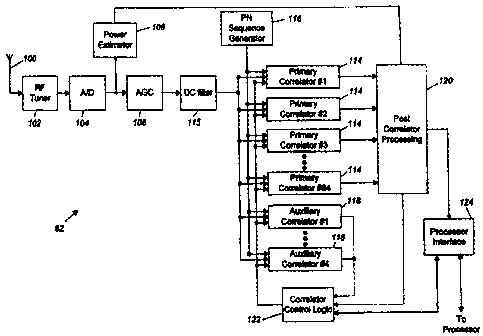
Referring now to FIGURE 6, the receiver 52 includes an
antenna 100 coupled to a standard RF tuner 102, which down
converts the received signal from the RF carrier to the IF
carrier and adjusts the power level of the signal, if
necessary, to ensure that it falls within a range suitable for
analog-to-digital (A/D) conversion. The down converted analog
signal then is provided to an A/D converter 109, which samples
the signal at a sampling rate (FS) eight times the chip rate of
CA 02294216 1999-12-22
WO 98/59446 PCT/US98/12919
- 12 -
the PN spreading sequence. In other words, for a 63-bit PN
sequence having a chip rate of 1.2 MHZ, the A/D converter 104
samples the incoming signal at a rate of approximately 9.6
MHZ, or eight samples per chip (8x over sampling). The A/D
converter 104 performs a "fixed conversion" which allows the
A/D converter 104 to output the sampled spread spectrum signal
at a second intermediate carrier frequency lower than the
sampling rate. Ideally, the second IF carrier frequency equals
approximately one-quarter the sampling frequency (FS/4).
Converting the incoming digital signal to FS/4 provides several
advantages, such as 1) allowing the use of an AC-coupled
filter 115 (or "DC block") to eliminate DC offset introduced
by the RF tuner 102, the A/D converter 104, and the AGC
circuit 106; 2) allowing the use of implementation efficient
bandpass correlators, as described below; and 3) allowing
extraction of the in-phase and quadrature components through a
de-interleaving process. The digital tuner 110 may down
convert the digital signal to any other fractional frequency
of the sampling frequency, provided that the upper end of the
digital signal's bandwidth remains below FS/2 and the lower end
of the bandwidth remains high enough to allow the AC-coupled
filter 115 to remove unwanted DC offset. The A/D converter 104
provides its digital output to an automatic gain control (AGC)
circuit 106, which keeps the amplitude of the digital signal
within an appropriate range, and to a power estimation block
108, which calculates the total energy of the digital signal.
The output of the power estimation block 108 is used by the
receiver 52 to evaluate whether a packet has been received, as
discussed below, and to provide information to an AGC
algorithm performed by the processor.
The digital signal, centered at FS/4, is provided to a
bank of eighty-four primary correlators 114, some of which are
used in each of the three stages (or "modes") of the
receiver's operation: search/qualification, acquisition, and
demodulation. Each of the primary correlators 114 compares the
incoming digital signal against a particular code phase of the
CA 02294216 1999-12-22
WO 98/59446 PCT/US98/12919
- 13 -
PN sequence, a copy of which is provided to the primary
correlator 114 by a PN sequence generator 116. As described in
- more detail below, the primary correlator 114 correlates the
incoming signal with the copy by multiplying the two signals
to form a product signal. If the code phases are aligned, the
product signal is a DC signal having a value of "1". Each
primary correlator 114 integrates its product signal over the
symbol period to form a correlation output, which generally
will have a high magnitude relative to noise if the signals
are aligned and a low magnitude relative to noise otherwise.
An implementation efficient bandpass correlator structure is
described in detail below.
The digital signal, centered at FS/4, also is provided
to four auxiliary correlators 118, which are used to verify
potential signal detections ("trips") produced during the
search/qualification mode, and to fine-tune the receiver to
the frequency of the incoming signal during the acquisition
mode. Each of the auxiliary correlators 118 should be able to
receive a copy of the PN sequence at any one of the possible
code phases and should be individually tunable over the
desired frequency range discussed below. The auxiliary
correlators 118 may use the implementation efficient bandpass
correlator structure described below.
A post-correlator processing block 120 continuously
monitors the outputs of the primary correlators 114 and
identifies correlation peaks, each of which indicates that the
code phase of the PN sequence in one of the primary
correlators 114 may have matched the incoming signal during a
symbol period. During the search/qualification mode, the
processing block I20 produces a trip signal indicating when a
correlation output may indicate a signal trip. The processing
block 120 also includes a series of comparators which, during
the demodulation mode, rank the correlation outputs during
each symbol period according to magnitude. This information is
used by the processor to demodulate the incoming data.
CA 02294216 1999-12-22
WO 98/59446 PCT/US98/12919
- 14 -
A correlator control logic block 122 controls
operation of the correlators during the three modes of
operation. The control logic block 122 includes a state
machine that steps through the three operation modes and
digital circuitry that supplies control signals to each of the
correlators 114 and 118, according to instructions from the
processor (not shown in FIGURE 6). A processor interface 124
allows the post-correlator processing block 120 and the
control logic block 122 to provide information to the
processor and allows the processor to provide instructions to
the correlator control logic block 122.
During the search/qualification mode, the receiver 52
must detect and recognize potential DSSS signals existing in
the wireless network. During the acquisition mode, the
receiver 52 must align to the transmission phase and frequency
of the incoming signal. During demodulation, the receiver 52
must determine whether it is the intended recipient of the
incoming signal and, if so, accurately demodulate the digital
data contained in the signal.
As discussed above, the DSSS signals transmitted in
the wireless network may consist of a carrier wave in the ISM
band multiplied by a 63-chip PN sequence. To acquire one of
these signals during the search and qualification mode, the
receiver 52 must correlate the received signal with a local
copy of the PN sequence that is almost perfectly aligned with
the code phase of the original PN sequence. However, at
minimal detectable signal levels the receiver 52 typically
cannot recognize that a signal is present until after code
phase alignment has occurred. Therefore, the process of
alignment must proceed by trial and error.
Further complicating the search process are potential
errors in the carrier frequency generated by the transmitter
or the receiver's tuning frequency. In a typical wireless
network the potential carrier error may be greater than ~50
kHz, so the receiver may need to search over a frequency range
greater than 100 kHz centered at the nominal carrier
CA 02294216 1999-12-22
WO 98/59446 PCT/US98/12919
- 15 -
frequency. In general, the receiver can detect signals only by
searching an area defined by the PN sequence length and the
carrier uncertainty by trial-and-error, and it must do so
within a time defined by the packet preamble, leaving enough
preamble time to align itself with the transmission phase of
the incoming signal.
Typically, each primary special correlator 114 will
respond with a maximum sensitivity loss of 4 dB to any signal
within ~3/8 chip and ~5 kHz of its code phase and frequency
settings. The measurement of a correlator's response will be
available once per symbol period, as described in more detail
below. Therefore, each primary correlator 114 can search an
area of 3/4 chip and 10 kHz during one symbol period. To
ensure that the entire 63-chip range is searched during each
symbol period and that the entire code/frequency range is
searched in a reasonable time, eighty-four primary correlators
114 are required [(63 chips) . (3/4 chip per correlator) - 84
correlators], each tuned to one of eighty-four search phases
separated by 3/4 chip.
The correlator control logic block 122 automates the
search process. The control logic 122 initializes each of the
primary correlators 114 to a corresponding one of the eighty-
four possible 3/4-chip search phases of the PN sequence and to
the nominal carrier frequency, as commanded by the processor.
The primary correlators 114 each include frequency adjustment
elements, as described below. Each primary correlator 114
correlates the corresponding search phase of the PN sequence
against the incoming digital signal for a symbol period, dumps
its correlation output, and immediately begins correlating
again against the digital signal over the next symbol period.
The search frequency of each primary correlator 114 is
increased by 10 kHz at the end of each symbol period until it
reaches the upper end of the carrier uncertainty range and
then is decreased by 10 kHz per symbol period until the lower
end of the range is reached, and so on, until a signal is
acquired.
CA 02294216 1999-12-22
WO 98/59446 PCT/US98/12919
- 16 -
The post-correlator processing block 120 monitors the
correlation outputs at the end of each symbol period and
generates a trip signal if any of the correlation outputs is
sufficiently high. The processing block 120 does not generate
a trip signal unless one of the correlation outputs,
normalized to the output of the power estimator block 108,
exceeds a predetermined threshold. This threshold depends
upon the characteristics of the network in which the receiver
52 is used, and factors such as the minimum detectable signal
level and the false trip rate may be taken into account.
When the correlator control logic block 122 receives a
trip signal, it commands one of the four auxiliary correlators
118 to qualify the trip while the primary correlators 114
continue searching. The control logic 122 sets the assigned
auxiliary correlator to the frequency at which the trip
occurred and instructs the PN sequence generator to provide
the auxiliary correlator 118 with a copy of the PN sequence at
the search phase associated with the trip. To qualify the
trip, the auxiliary correlator correlates the incoming digital
signal against the PN sequence at the selected search phase
over successive symbol periods. The correlation over a given
symbol period is a "success" if the correlation output of the
auxiliary correlator 118, normalized to the output of the
power estimator block 108, exceeds a predetermined threshold.
The trip is qualified after three consecutive successful
symbol periods. On the other hand, the auxiliary correlator
118 drops the trip and ends qualification after three
consecutive unsuccessful correlating periods or after twelve
symbol periods have passed without qualification. If no
auxiliary correlators 118 are available when a trip signal
occurs (i.e., if all four auxiliary correlators 118 are busy
qualifying trips), the receiver queues the trip. When a trip
signal is qualified, the primary correlators 114 stop
searching and the receiver 52 enters the acquisition mode.
The acquisition mode consists of two phases: fine code
search and fine frequency search. During fine code search, the
CA 02294216 1999-12-22
WO 98/59446 - PCT/US98/12919
- 17 -
receiver 52 sets each primary correlator 114 to the frequency
of the qualified trip and sets each of the first sixteen
primary correlators 114 to sixteen consecutive phases of the
PN sequence separated by one sample. The eighth correlator
correlates against the search phase of the qualified trip; the
seven preceding correlators correlate against the seven
phases, each separated by one sample, immediately preceding
the search phase of the qualified trip; and the eight
following correlators correlate against the eight phases, each
separated by one sample, immediately following the search
phase of the qualified trip. The sixteen correlators collect
data for one symbol period, with each correlator's correlating
period offset a sample behind the correlating period of the
preceding correlator.
The outputs of the sixteen correlators undergo a
special fine code correlation against an ideal relationship
between code phase error and correlator response. This special
correlation indicates which offset from the code phase of the
qualified trip most closely correlates to the ideal response,
which is considered over a range of ~4 samples from perfect
code alignment. A normalized ideal response (R) at each sample
offset is represented by the following equation:
R; _ ( 1 - 64i/504)2,
where i is the offset in samples and -4 _< i <_ 4. The
correlation (C) of each sample offset against the ideal
response then is determined by the following equation:
C~ - ~ Ri '0~,~,"
where Ok is the output of the kth correlator (0 <_ k < 16), where
i and j represent the offset in samples (-4 _< i,j _< 4). For j
- -4 and i = -4, "i + j" is less than zero, so the special
correlation value at these offset values is disregarded. The
best-fit code phase is the one for which the corresponding
correlation value (C~) is largest ("code phase zero" or "data
phase zero"). The receiver 52 continues to qualify any
outstanding search trips during fine code search but
CA 02294216 1999-12-22
WO 98/59446 PCT/US98/12919
- 18 -
terminates trip qualification when the fine code search stage
is successful.
In the fine frequency search phase, which begins after
the fine code search is successful, the four auxiliary
correlators I18 are used to find the peak of the frequency
response to the incoming signal. Each of the auxiliary
correlators 118 is set to code phase zero, as determined in
the fine code search phase, and to one of several frequencies
near the frequency of the qualified trip. Each auxiliary
correlator 118 then provides an output representing a point on
a frequency response curve, the peak of which represents the
signal frequency and may be calculated by the processor.
The receiver 52 also incorporates false peak rejection
to ensure that it does not lose valid data packets after
detecting and qualifying "false" peaks that may occur at code
phases and/or frequencies other than the actual phases and
frequencies of the true signals. The processor will recognize
a false peak when the signal-to-noise (S/N) ratio of the
tripping signal does not improve beyond -13 dB during the fine
code and fine frequency search phases. To reject false peaks
and to avoid subsequent trips on false peaks from the same
signal, the processor drops any signal for which the S/N ratio
has not improved by 12 dB after the fine code and fine
frequency search phases and sets the trip threshold 6 dB
higher than normal during the subsequent search process.
Increasing the threshold in this manner should allow the
receiver 52 to detect the true peak of a strong signal while
ignoring the false peaks.
When the fine code and fine frequency search phases
are complete, the receiver 52 begins watching for the sync
word. Because the sync word is encoded with 2-CCSK modulation,
as described above, the correlator control logic 122 assigns
only two primary correlators 114 to monitor the incoming
signal for the sync word. The two assigned correlators are the
correlator associated with code phase zero, as determined in
the fine code search phase, and the correlator immediately
CA 02294216 1999-12-22
WO 98/59446 PCT/US98/12919
- 19 -
following it. The two correlators then correlate the incoming
signal against the corresponding code phase over the same
correlation period. The correlation outputs of the two
correlators are provided to the processor, which assigns each
symbol in the sync word a soft value S; according to the
equation:
- ( A; - B~ ) / ( A; + B; ) .
where A; and B; represent the correlation outputs of the two
correlators at each symbol period. The processor stores up to
thirteen soft values and, after each symbol period, forms a
correlation sum (C) according to the equation:
~=~S~-a~,
where the sum runs from i = 0 to 12 and where (3; represents the
actual value of the ith bit of the synch word, with logic
levels of ~l. The signal is declared synchronized when the
correlation sum is greater than some predetermined threshold.
During the demodulation mode, sixteen of the primary
correlators 114 correlate the incoming digital signal to the
sixteen different code phases defining the 16-CCSK symbol
alphabet, with the first correlator corresponding to code
phase zero, as determined during the fine code search phase,
and the following correlators successively corresponding to
the other fifteen code phases. All sixteen correlators use the
same correlation period in the demodulation mode. At the end
of each symbol period, the post-correlator processor block 120
determines which correlators have the highest correlation
outputs. The processor assigns a symbol value to the symbol
period based on which correlator produces the highest
correlation output. The processor may be programmed so that it
does not assign a symbol value (i.e., it issues an "erasure")
if the ratio of the highest correlation output to the second
highest correlation output does not exceed some predetermined
threshold.
During demodulation, the receiver also tracks the code
phase of the incoming signal. Code phase tracking ensures that
the receiver does not lose alignment with the signal as a
CA 02294216 1999-12-22
WO 98/59446 _ PCT/US98/12919
- 20 -
result of clock drift that may affect the output of the PN
sequence generator 116. To track the code phase, the
correlator control logic 122 assigns thirty-two additional
primary correlators 114, half of which provide "early"
correlation values and the other half of which provide "late"
correlation values. Each "early" correlator is set to a code
phase that is between one and four samples ahead of the code
phase associated with one of the main demodulation correlators
("on-phase" correlators) discussed above. Each "late"
correlator is set to a code phase that is between one and four
samples behind the code phase associated with one of the on-
phase correlators. The receiver 52 uses the correlation
outputs of the early and late correlators associated with the
on-phase correlator aligning to the incoming signal during
each symbol period to calculate a code phase error (R),
according to the equation:
R = ( E - L) / 0,
where E and L are the outputs of the early and late
correlators and O is the output of the on-phase correlator.
The code phase error may be used to update the clocking rate
of the PN sequence generator 116 when the error is, e.g.,
greater than 1/16 chip.
Referring also to FIGURES 7A and 7B, the receiver
begins operation upon startup by initializing the automatic
gain control circuit (step 300). The receiver then enters the
search mode (step 302) and continuously searches for a DSSS
signal, constantly monitoring and adjusting the AGC circuit
(step 304), until a trip signal occurs (step 306). When a trip
signal occurs, the receiver determines whether all of the
auxiliary correlators are busy (step 308). If so, the receiver
queues the trip signal (step 310) and continues searching
(step 302); otherwise, the receiver assigns an auxiliary
correlator to qualify the trip (step 312). The receiver then
monitors the qualification process to determine whether the
trip signal is qualified or rejected within the allotted
period of time (steps 314 and 318). If neither qualification
CA 02294216 1999-12-22
WO 98/59446 _ PCT/US98/12919
- 21 -
nor rejection occurs within twelve symbol periods, the
receiver aborts the qualification process for that trip signal
(step 316) and continues searching for DSSS signals (step
302). The receiver also continues searching if the trip signal
is disqualified (step 318). If, on the other hand, the
auxiliary correlator qualifies the trip signal, the receiver
enters the acquisition mode.
In the acquisition mode, the receiver first assigns
several primary correlators to carry out the fine code search
(step 320). The receiver then monitors the assigned
correlators to determine whether the code phase is
successfully acquired (step 322). If not, the receiver returns
to the search mode and resumes its search for DSSS signals
(step 302); otherwise, the receiver instructs the auxiliary
correlators to enter the fine frequency search phase (step
324). The receiver then monitors the four general correlators
to determine whether the fine frequency search leads to
successful acquisition of the frequency offset (step 326). If
not, the receiver returns to the search mode and resumes
searching (step 302); otherwise, the receiver prepares for
sync word detection (step 328). If the expected sync word is
not detected within the appropriate time limit, the sync word
detection process times out (step 330) and is aborted (step
316), and the receiver again begins searching for DSSS signals
(step 302). If the sync word is detected, the receiver enters
the demodulation mode (step 332). In the demodulation mode,
the receiver continuously tracks the code phase of the
incoming data signal to prevent drift in alignment (step 334).
If too many erasures occur during demodulation (step 333), the
demodulation process is aborted (step 316) and the receiver
again searches for DSSS signals (step 302). Otherwise, the
receiver continues to demodulate data until the end of the
transmitted packet (step 336). When the end of the packet is
reached, the receiver leaves the demodulation mode, reenters
the search mode, and again begins searching for DSSS signals
(step 302).
CA 02294216 1999-12-22
WQ 98/59446 - PCT/US98/12919
- 22 -
Referring now to FIGURE 8A, each bandpass correlator
(primary and auxiliary) in the receiver may utilize an
implementation efficient (IE) correlator structure 130. As
discussed above, the incoming digital signal 131 should enter
the correlator at a carrier frequency equal to approximately
one-quarter the digital sampling rate (FS/4). The IE correlator
structure provides approximate quadrature processing and
frequency adjustment in a unified block that requires few and
inexpensive components. The structure includes a digital
multiplier 132 followed by an accumulation loop 134 having a
primary summer 136 and two delay elements 138 and 140, both of
which may be single sample delay registers. The output 141 of
the second delay register 140 feeds back to the primary summer
136 and is subtracted from the product output 135 of the
multiplier 132. The output 139 of the first delay register 138
feeds directly into the second delay register 140. Output 139
also may be provided to a frequency adjustment element 145
that allows the processor to adjust the resonant frequency of
the accumulation loop 134. Within the frequency adjustment
element 145, the output 139 of the first delay register 138 is
scaled by a scaling element 144, fed back to a secondary
summer 142, and added to the output 137 of the primary summer
136. The correlator structure 130 may be implemented in
standard, off-the-shelf components, but it is particularly
suited for implementation in an application specific
integrated circuit (ASIC).
In operation, the incoming digital signal 131 and a
local copy of the PN sequence I33 are provided as inputs to
the multiplier 132. If the two are in code phase alignment,
the code product always equals "1" and the output 135 of the
multiplier is simply the FS/4 carrier wave. Because the loop
delay is two samples, the output 141 of the second delay
register 140 is approximately 180° out-of-phase with the
multiplier output 135 and therefore reinforces the multiplier
output 135 in the primary summer 136 during the subtraction
operation. The input 143 and the output 149 of the first delay
CA 02294216 1999-12-22
WO 98/59446 - PCT/US98/12919
- 23 -
register 138 differ by one sample time and therefore are
approximately 90° out-of-phase, so they may be taken as the in-
phase and quadrature components, respectively, of the FS/4
carrier wave. At the end of the accumulation time (one
correlation period), the in-phase and quadrature outputs are
taken and the delay registers 138 and 140 both are set to zero
to re-initialize the accumulation loop 134. The final output
151 is the sum of the squares of the in-phase and quadrature
components at the end of each correlation period, as provided
by squaring circuits 146 and 148 and adder 150.
Instead of a single-sample, register 140 may delay
output 139 by multiple samples, so that the phase offset
between output 135 and output 141 is a multiple of 180°. For
example, a three sample delay in register 140 leaves output
141 360° out-of-phase with product output 135. In this case,
primary summer 136 will add output 141 to product output 135
to form an accumulation output.
The frequency adjustment element 145 includes a
scaling element 194, the scaling factor (K) of which is
variable to allow for frequency adjustment within the
correlator's accumulation loop 134. The scaling factor K has a
value equal to 2~cos (S2o) , where S2o represents 2n times the ratio
of the desired resonant frequency of the accumulation loop 134
to the sampling rate (FS) of the A/D converter 109 (the
absolute value of K typically will be much less than one).
The value of the scaling factor may be selected by the
processor and stored in a programmable storage element 144b
such as a register. A multiplication element 144a applies the
scaling factor to the output 139 of the first delay register
138, and the resulting signal is added by the secondary summer
142 to the output 137 of the primary summer 136. When the
scaling factor has a value of zero, the secondary summer 142
has no effect on the correlator structure. However, when the
scaling factor is slightly above or below zero, the effective
delay in the accumulation loop 134 is slightly greater than or
less than two samples, so the loop response is centered at a
CA 02294216 1999-12-22
W0.98/59446 - _ PCT/US98/12919 _
- 24 -
frequency slightly below or slightly above FS/4. Since the
delay between the output 139 of delay element 138 and the
output 141 of delay element 140 always remains at one sample,
adjusting the scaling factor to a value other than zero
introduces a small quadrature error at frequencies offset from
FS/4. At small frequency offsets, the quadrature error is
insignificant.
Referring to FIGURE 8B, a quadrature error correction
element 160 may be added to the correlator structure 130 to
eliminate the quadrature error introduced by the scaling
element 144. The correction element 160 includes two
multiplication elements 162 and 164, which multiply the output
139 of the accumulation loop 134 with signals equal to cos(S2o)
and sin(~2o). The output 165 of multiplication element 164
represents the corrected quadrature component of the
accumulation output and is provided to squaring circuit 148.
Summer 166 produces the corrected in-phase component of the
accumulation output by subtracting the output 163 of
multiplication element 162 from the output 143 of secondary
summer 142. The corrected in-phase component is provided to
squaring circuit 146.
Referring also to FIGURE 9, when a binary PN sequence
serves as the spreading signal, the digital multiplier 132 may
be a simple sign inverter realized, e.g., as a digital
multiplexes 155 receiving the incoming digital signal 131 and
an inverted version 131' of this signal as inputs and having a
local copy of the PN sequence 133 as its control signal. The
non-inverted signal 131' is selected by the multiplexes 155
when the PN sequence 133 is high, and the inverted signal 131'
is selected when the PN sequence 133 is low. When the incoming
signal 131 and the PN sequence 133 are aligned, the PN
sequence cancels the spreading signal from the incoming signal
131 and only the FS / 4 carrier wave exits the multiplexes 155.
Other embodiments are within the scope of the
following claims.