Note: Descriptions are shown in the official language in which they were submitted.
CA 02294715 1999-12-29
WO 99/02753 PCT/CA98/00645
APPARATUS AND METHOD FOR NUCLEATION AND DEPOSITION OF
DIAMOND USING HOT-FILAMENT DC PLASMA
FIELD OF THE INVENTION
The present invention relates to the field of chemical vapor
deposition (CVD) of diamond films, and more particularly, to a method and
apparatus for nucleation and growth of diamond films by hot filament DC plasma
CVD.
BACKGROUND OF THE INVENTION
Hot filament chemical vapor deposition (HFCVD) has been
extensively used by researchers to deposit polycrystalline diamond on a
variety
of substrates. The technique and reactor designs typically used for HFCVD of
diamond are described in detail in an article entitled "Growth Of Diamond
Particles From Methane-Hydrogen Gas" published in J. Materials Science 17,
3106(1982) by Matusumoto et al. Since this disclosure, numerous researchers
have attempted to improve the HFCVD technique. This development can be
found in the review article by C.E. Spear entitled "Diamond-ceramic coating of
the future" published in J. Am. Ceram. Soc. 72(2), 171(1989). The reactor
generally comprises a resistively heated filament and a heated or cooled
substrate stage which are housed in a reactor chamber with pumping and
pressure monitoring facilities. The filament is made from a high melting-point
refractory metal that is used to dissociate hydrogen and other molecules in a
feed gas which normally contains a mixture of hydrogen and hydrocarbon.
Atomic hydrogen and other dissociated products subsequently react with the
feed gas to generate precursors responsible for diamond formation. The
precursors then diffuse to and condense on the substrate for the formation of
polycrystalline diamond. The separation between the filament and the substrate
is normally in the range 0.5 to 5cm. With this small distance, a sufficient
amount
of growth precursors diffuses to the substrate prior to their recombination
into
1
CA 02294715 2006-08-21
more stable molecules.
A major advantage of HFCVD of diamond films, relative to other
methods of diamond film growth such as microwave plasma CVD (MWCVD),
radiofrequency CVD, and plasma jet CVD, is the low equipment investment
costs, and the ease in scaling up the production to a large area substrate.
The diamond growth rate using HFCVD does not normally exceed 5,um/hr
and is typically about 1 m/hr (see e. g., International PCT Patent
Publication
WO 91/14798 (1991), by Garg, et al., entitled"An Improved Hot Filament
Chemical Vapor Deposition Reactor"), which is not high enough for
economically viable thick film production. A major disadvantage of HFCVD, as
with other known diamond growth methods, is that it requires scratching or
diamond-seeding of the substrate surface to initiate diamond nucleation.
Such a pretreatment induces a high defect concentration on the substrate
surface and thus generally precludes the possibility of obtaining
heteroepitaxial growth of diamond. This pretreatment increases the CVD
diamond production costs.
A method of achieving nucleation enhancement is disclosed by
Yugo et al. in an article entitled"Generation Of Diamond Nuclei By Electric
Field In Plasma Chemical Vapor Deposition" and published in Applied
Physics Letters 58 (10), 1036-1038 (1991) which proposes a predeposition of
diamond nuclei on a silicon mirror surface prior to the conventional diamond
CVD growth process. Yugo et al. reported that diamond nuclei growth
required a high methane content in hydrogen and did not occur below 5%,
and that high densities of nuclei occurred only above 10% methane. Yugo et
al. also reported that the substrate bias against'the CVD plasma should be
below 200 volts to avoid sputtering and the typical bias was 70 volts. The
total
time duration for the pretreatment was limited to between 2 to 15 minutes.
More recently, Stoner et al. (see e. g., World Patent # 93/13242
(1993), entitled"Nucleation Enhancement For Chemical Vapor Deposition Of
Diamond") and Jiang et al. (see e. g.,"Epitaxial Diamond Thin Films On (001)
Silicon
2
CA 02294715 2006-08-21
Substrates", Applied Physics Letters 62 (26), 3438-3440 (1993)) have
independently disclosed diamond nucleation enhancement by negatively
biasing the substrate against the CVD plasma during MWCVD of diamond
films on silicon. More importantly, both of these groups showed that the
preservation of the crystallinity of the silicon substrate surface as a result
of
the elimination of ariy scratching/diamond-seeding pretreatment, together with
the nucleation enhancement, allows the heteroepitaxial formation of diamond
(100) nuclei on Si (100). In the method described by Jiang, et al., the
substrate was biased at -100 to -300 V relative to the microwave plasma with
a typical recipe for MWCVD of diamond using CH4/H2. In the method
described by Stoner et al., the negative bias of the substrate required for
nucleation enhancement was claimed to be not less than 250 volts. The
nucleation of diamond and heteroepitaxial nucleation of diamond with a
modified HFCVD-DC plasma method and apparatus, which require much less
equipment investment than the MWCVD approach, is one advantage of the
present invention discussed hereinafter.
Modifications of the conventional HFCVD by coupling it with DC
plasma CVD have been proposed previously by A. lkegaya and T. Masaaki in
JP 173366 (1986), JP 75282 (1987), and European Patent Publication
0254312 Al (1988). In this approach, a hot filament array is used as a
thermionic electron emitter and a grid electrode is inserted between the hot
filament array and the substrate. The filament array and the substrate are
both negatively biased against the grid electrode in order to form two DC
plasma zones, one between the filament array and the grid electrode, and the
other between the grid electrode and substrate. In these two plasma zones,
the plasma density in the grid-filament zone is much higher than that between
the grid-substrate zone because of thermionic electron emission from the hot
filaments. In the grid-filament zone, ions are extracted towards the
filaments,
i. e., further away from the substrate. Through gas phase collision, this
extraction will also move the reactants generated near the filament away,
instead of towards, the substrate. lkegaya et al. reported a growth rate of
3
CA 02294715 2006-08-21
2/.cm/hr on a tungsten carbide substrate using 1% methane in hydrogen, a
power density of 40W/cm2 between the hot filament and grid and 20W/cm2
between the grid and substrate with a hot filament temperature of about
2000 C and a substrate temperature of 980-1010 C and a pressure of 90
torr. A growth rate of 12.5um/hr was also reported for a gas mixture of 2%
(CH3)2CN in H2 with a power density of 60 W/cm2 between the filament and
grid, and a power density of 40 W/cm2 between the grid and substrate.
lkegaya et al. noted that a DC plasma power density higher than 200 W/cm2
between the grid and substrate led to sputter-etching of the substrate.
Ikegaya et al. reported that this problem arises because the negative bias on
the substrate against the grid attracts ions to the substrate. A high DC
plasma
power density results in a high bombardment energy and high current density,
and the induced energetic particle bombardment causes detrimental sputter-
etching.
A logical approach for eliminating the sputtering problem is to
connect the substrate to the grid or simply to discard the grid. A DC plasma
can still be maintained by biasing the filament negatively against the
substrate. In fact, A. Ikegaya and N. Fujimori showed such a configuration in
a JP 176762 and a PCT Patent Publication W092/01828 (1992). However, a
drawback to both of these designs is that they do not allow for any ion
extraction towards the substrate during nucleation and growth.
Thus, there still exists a need to modify the HFCVD method and
apparatus in order to provide an economical approach to control energetic
particle bombardment for improved diamond nucleation and growth.
SUMMARY OF THE INVENTION
The present invention discloses a method and apparatus to
nucleate diamond in a high density on substrates without any scratching or
diamond-seeding requirement, and to efficient grow diamond coatings at high
growth rates. The design of the method and apparatus takes into account the
4
CA 02294715 2003-06-25
limitations of the aforementioned hot filament DC plasma devices and
processes.
The present invention provides a method of growing a diamond film
by hot filament discharge comprising positioning a substrate having a
deposition
surface on a substrate holder in a vapor deposition chamber, providing a grid
electrode spaced from the substrate deposition surface and providing a
filament
array electrode interposed between the grid electrode and the substrate
deposition surface. The method includes flowing a gas mixture comprising
hydrogen and gas containing carbon into the vapor deposition chamber and
resistively heating the filament array electrode to a temperature in a range
of from
about 1800 C to about 2600 C with the substrate being heated to a temperature
in the range from about 600 C to about 1100 C. The method includes nucleating
the substrate by biasing the filament array electrode at a positive voltage
with
respect to the substrate holder, and biasing the grid electrode at a voltage
positive with respect to the filament array electrode to provide an effective
potential drop between the grid electrode and the substrate for efficient ion
extraction toward the substrate. Thereafter the grid electrode is biased at a
voltage positive with respect to the voltage on the filament array electrode
to grow
a diamond film on the deposition surface.
During the step of nucleating the substrate the substrate may be
biased at ground potential and the filament array electrode biased to a
potential in
a range from about 20 to about 300 Volts with respect to the substrate holder.
The grid electrode is biased to a voltage in a range from about 20 to about
300
Volts with respect to the filament array electrode.
During the step of growing the diamond film after the step of
nucleating, the substrate holder and filament array electrode may be biased at
ground potential and the grid electrode biased at a voltage in a range from
about
20 to 300 Volts with respect to the filament array electrode.
Alternatively, during the step of growing the diamond film after the
step of nucleation the substrate holder may be biased at ground potential and
the
5
CA 02294715 2003-06-25
filament array electrode biased at a negative voltage with respect to the
substrate
holder wherein the negative voltage being in a range from about -20 to about -
300
Volts with respect to the substrate holder.
In another aspect the present invention provides a method of
growing a diamond film by hot filament discharge comprising positioning
substrates each having a deposition surface on first and second spaced
substrate
holders in a vapor deposition chamber, providing a grid electrode located
between the first and second substrate holders and a first filament array
electrode
interposed between the first substrate holder and the grid electrode and a
second
filament array electrode interposed between the second substrate holder and
the
grid electrode. The method includes flowing a gas mixture comprising hydrogen
and gas containing carbon into the vapor deposition chamber and resistively
heating the first and second filament array electrodes to a temperature in a
range
of from about 1800 C to about 2600 C, the substrates being heated to a
temperature in the range from about 600 C to about 1100 C. The method
includes nucleating the substrates on the first and second substrate holders
by
biasing the first fiiament array electrode at a positive voltage with respect
to the
first substrate holder to provide a plasma having an effective potential drop
between the grid electrode and the first substrate for efficient ion
extraction in the
plasma toward the substrates on the first substrate holder, and biasing the
grid
electrode at a voltage positive with respect to the voltage on the second
filament
array electrode to provide a plasma having an effective potential drop between
the grid electrode and the second substrate for efficient ion extraction in
the
plasma toward the substrates on the second substrate holder. Thereafter the
grid
electrode is biased at a voltage positive with respect to the voltage on the
first and
second filament array electrodes to grow a diamond film on the deposition
surfaces of the substrates on the first and second substrate holder.
In another aspect the present invention provides a method of
growing a diamond film by hot filament discharge, comprising positioning
substrates each having a deposition surface on first and second spaced
substrate
6
CA 02294715 2003-06-25
holders in a vapor deposition chamber, providing a first filament array
electrode
spaced from the first substrate holder and a second filament array electrode
interposed between the first filament array electrode and the second substrate
holder; flowing a gas mixture comprising hydrogen and gas containing carbon
into
the vapor deposition chamber and resistively heating the first and second
filament
array electrodes to a temperature in a range of from about 1800 C to about
2600 C, the substrates being heated to a temperature in the range from about
600 C to about 1100 C; and biasing the first and second filament array
electrodes and the first and second substrate holders to produce a plasma to
grow a diamond film on the deposition surface of substrates on the first and
second substrate holders.
In another aspect of the invention there is provided a hot filament
DC discharge plasma apparatus for synthesizing a diamond film. The apparatus
comprises a deposition chamber having a gas inlet for flowing reactant gases
into
the deposition chamber; a conducting substrate holder adapted to support a
substrate having a surface on which the diamond film is to be synthesized,
and means for heating and cooling the substrate holder. The apparatus includes
a grid electrode spaced from the surface of the substrate holder; a filament
array
electrode interposed between the grid electrode and the substrate holder, and
includes means for resistively heating the filament array electrode. The
apparatus
includes means for biasing the grid electrode, the filament array electrode
and the
substrate holder to produce a hot filament DC discharge plasma. The means for
biasing includes means for adjusting the bias potential on the grid electrode
and
the filament array electrode relative to the substrate holder and each other.
In another aspect of the invention there is provided a hot filament
DC discharge plasma apparatus for synthesizing a diamond film, comprising
a deposition chamber having a gas inlet for flowing reactant gases into the
deposition chamber; first and second spaced conducting substrate holders each
adapted to support a substrate having a surface on which the diamond film is
to
be synthesized, and means for heating and cooling the first and second
substrate
7
CA 02294715 2003-06-25
holders. The invention includes a grid electrode located between the first and
second substrate holders; a first filament array electrode interposed between
the
first substrate holder and the grid electrode and a second filament array
electrode
interposed between the second substrate holder and the grid electrode. The
apparatus includes means for resistively heating the first and second filament
array electrodes. The apparatus is provided with power supply means for
biasing
the grid electrode, the first and second filament array electrodes and the
first and
second substrate holders to produce a hot filament DC discharge plasma and
including means for adjusting the bias potential on the grid electrode, and on
the
first and second filament array electrodes relative to each other and to the
first
and second substrate holders respectively.
In another aspect the present invention provides a hot filament
discharge plasma apparatus for synthesizing a diamond film comprising
a deposition chamber having a gas inlet for flowing reactant gases into the
deposition chamber; first and second spaced conducting substrate holders each
adapted to support a substrate having a surface on which a diamond film is to
be
synthesized, and means for heating and cooling first and second substrate
holders. The apparatus includes a first filament array electrode spaced from
the
first substrate holder and a second filament array electrode interposed
between
the first filament array electrode and the second substrate holder, and means
for
resistively heating the first and second filament array electrodes. The
apparatus
includes means for biasing the first and second filament array electrodes and
the
first and second substrate holders to produce a hot filament discharge plasma
and includes means for adjusting the bias potential on the first and second
filament array electrodes relative to each other and to the first and second
substrate holders respectively.
More particularly, in the present invention a hot filament is placed
between a grid electrode and the substrate. The plane of the grid is parallel
to the
plane of filament. The grid can be either parallel wires, or rods, or mesh, or
plate
with holes. The grid can be either cooled or heated. The direction of the
elements
7a
CA 02294715 2003-06-25
of the grid (wires or rods) can be either perpendicular or parallel, or at any
angle
to the direction of filament. The distance between the hot filament and
substrate
is preferably less than 2 cm, and the distance between hot filament and grid
is
preferably less than 5 cm. When the distance between the hot filament and grid
is
set equal to zero, the hot filament and grid are in the same plane. In the
normal
operation of the system, the growth substrate holder
7b
CA 02294715 1999-12-29
WO 99/02753 PCT/CA98/00645
is preferably biased at ground potential. The power density for resistively
heating the filaments is about 20 - 500 W/cm2. During nucleation of diamond,
the
filaments are biased positively at 20-300 Volts relative to the substrate
holder
and the grid electrode is biased positively in the range of 20-300 Volts
relative to
the filament array. As such, a DC plasma can be maintained between the grid
and filaments. Ions in the plasma are extracted towards the substrate for
particle
bombardment assisted nucleation. The nucleation process typically takes less
than ten minutes. During diamond nucleation, a plasma is maintained between
the filaments and grid with the thermionic emission from the hot filament
cathode
to enhance the plasma density. The unique substrate-hot filament-grid
configuration of the present invention allows the maintenance of the substrate
at
a potential even more negative than the hot filament cathode such that
effective
ion extraction towards the substrate can be induced for the enhanced diamond
nucleation.
During diamond growth, the substrate holder may be biased at
ground potential. The filament array is either not biased at all or biased
negatively relative to the substrate holder. The negative biasing voltage on
the
filament array is normally -20 to -300 Volts. The grid is biased positively at
20-
300 Volts relative to the filament array. The typical plasma energy density is
about 1 - 300 W/cm2. When the filaments are not biased, a DC plasma will be
mainly maintained between the grid and filaments. The large cathode voltage
drop near the filament will draw some ions from the plasma towards the
filaments. Due to the small mean free path for collision in the processing
pressure (about 0.01 mm at 50 Torr and 1500K), such an ion extraction in the
direction towards the substrate will result in the partitioning of the ion
energy into
kinetic energy for neutrals in the collision cascades. In turn, these
accelerated
neutrals will have a net average velocity towards the substrate, and have an
average energy higher than the average thermal energy in the system, and can
thus enhance the reaction probability towards diamond growth. But the average
8
CA 02294715 1999-12-29
WO 99/02753 PCT/CA98/00645
energy will be much less than a few electron volts, which is not sufficient
for
inducing any significant sputtering action on the substrate. The motion of
neutrals towards the substrate enhances the arrival rate of the precursors
beyond that induced by simple diffusion, and enhances the diamond growth rate.
With the filament array biased at a negative potential relative to the
substrate holder, a DC plasma can also be maintained between the filament
array and substrate. However, a high DC power input in this operation mode
may lead to the raise of the substrate surface temperature outside the diamond
growth window, which is a limitation common to other prior arts of hot
filament
DC plasma techniques. Accordingly, under the normal operation in the present
invention, the plasma power input between the grid and filaments is higher
than
that between the filaments and substrate.
BRIEF DESCRIPTION OF THE DRAWINGS
The method and apparatus for growing diamond coatings using the
hot-filament DC plasma method according to the present invention will now be
described, by way of example only, reference being had to the accompanying
drawings, in which:
Figure 1 is a schematic diagram of a conventional HFCVD reactor
according to typical configurations of prior art;
Figure 2 is a schematic diagram of a hot filament DC plasma CVD
reactor with a typical filament-grid-substrate configuration of prior art;
Figure 3 is a schematic diagram of the apparatus according to the
present invention;
Figure 4 is a schematic diagram of an apparatus for depositing
diamond coatings onto multiple substrates according to the present invention;
Figure 5 is a schematic diagram of another embodiment of an
apparatus for depositing diamond coatings;
Figure 6a is an optical micrograph of heteroepitaxially grown
9
CA 02294715 1999-12-29
WO 99/02753 PCT/CA98/00645
diamond on Si (diamond (100)//Si(100), diamond [110]//Si[110]) produced by
the present invention in a low nucleation density mode; and
Figure 6b is an optical micrograph of heteroepitaxially grown
diamond on Si (diamond (100)//Si(100), diamond [110]//Si[110]) produced by
the present method in a high nucleation mode.
DETAILED DESCRIPTION OF THE INVENTION
Prior Art
A schematic representation of a typical HFCVD reactor used in
prior art diamond growth processes is shown in Figure 1. The reactor 10
comprises a chamber 12 enclosing a resistively heated filament 14 and a heated
or cooled substrate holder 16 on which a substrate 17 is placed. Pumps and
pressuring monitoring equipment is included (not shown). The reactant gas
mixture is fed into the chamber through a gas diffuser unit 18. The filament
14 is
made from a high melting-point refractory metal, such as tungsten or tantalum,
and is heated to between 1800 - 2300 C to dissociate hydrogen and other
molecules in the reactant gas mixture which normally contains a mixture of
hydrogen and hydrocarbon. Atomic hydrogen and other dissociated products
subsequently react with the reactant gas mixture to generate precursors
responsible for diamond formation. The precursors then diffuse to and condense
on substrate 17 for the formation of polycrystalline diamond. The separation
between the filament and the substrate is normally in the range of 0.5 to 5
cm.
The temperature of the substrate is generally maintained in the range of 700
to
1000 C. The deposition rate and reaction efficiency are determined by a
combination of the rate of reactant generation near the filaments, the rate of
reactant diffusion to the substrate, and the probability of diamond formation
on
the substrate.
Figure 2 illustrates several modifications of the conventional
HFCVD by coupling the process with direct current (DC) plasma CVD as
CA 02294715 2006-08-21
proposed by A. Ikegaya and T. Masaaki in JP 173366 (1986), JP 75282
(1987), and European Patent 0254312 Al (1988). Referring to Figure 2, in
this approach, a hot filament 20 is used as a thermionic electron emitter and
a
grid electrode 22 is inserted between the hot filament 20 and the substrate
24. The filament 20 and the substrate 24 are both negatively biased against
the grid electrode 22 using power supplies 26 in order to form a DC plasma
between the. filament 20 and grid 22, and the grid 22 and substrate 24.
Present Invention
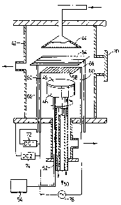
Figure 3 is a schematic diagram of an apparatus 40 for
implementing the method of nucleating and growing diamond in accordance
with the present invention. The reactant gas mixture is introduced into a
deposition chamber 42 through a gas shower unit 44. The substrate 46 on
which the diamond film is being deposited is placed on a substrate holder 48
which may be heated or cooled by a heat exchange fluid running through
conduits 50. The substrate holder 48 is equipped with a thermocouple 52 for
sensing the temperature of the substrate holder and may be connected to a
substrate temperature controller 54 that controls the temperature of the heat
exchange fluid.
A filament array 58 is mounted on conducting rods 60 and is
spaced above substrate holder 48. A grid electrode 64 is mounted on
conducting rods 66 and is spaced above filament array 58 so that a
sequential grid-filament- substrate assembly is provided. The filament array
58 is preferably spaced less than 2 cm from the top of substrate 46. The grid
electrode 64 is preferably spaced less than 5 cm from filament array 58. Grid
electrode 64 is shown as a wire grid in Figure 3 but may also be constructed
from a wire mesh, metal rods or a perforated metal plate able to withstand the
operating temperatures.
Filament array 58 is comprised of a plurality of conductive metal
filaments with a high melting point such as Ta and W. Filament array 58 can
withstand resistive heating to temperatures above 2000 C, the preferred
11
CA 02294715 1999-12-29
WO 99/02753 PCT/CA98/00645
temperature range for dissociating hydrogen in the reactant gas. Grid
electrode
64 and filament array 58 are shown as being substantially parallel.in chamber
42
but it will be appreciated that these components do not need to be parallel to
each other.
DC power supplies 72 and 74 are used to provide the DC bias
requirements during substrate nucleation and diamond coating growth. More
specifically, power supply 74 is used to maintain the bias requirements
between
the filament array 58 and substrate 46 and power supply 72 provides the bias
requirements between the grid electrode 64 and filament array 58. It will be
understood that the substrate on which the diamond film is being deposited is
typically electrically conductive so the substrate will be biased to the same
potential as the substrate holder. During diamond deposition the filament
array
58 is maintained in the temperature range of 1800-2600 C using a power supply
78 which is preferably an AC power supply. The power density is about 20-500
W/cm2. The plasma power density during growth is about 1-300W/cm2 . The grid
electrode 64 may be either heated or cooled during deposition of the diamond
film. The grid electrode 64 may be heated resistively and/or by plasma energy.
Grid 64 may comprise hollow rods and may be cooled by running a heat
exchange fluid through the centre of the electrode rods.
The temperature of filament array 58 and grid electrode 64 is
monitored by an optical pyrometer (not shown) which is located outside the
deposition chamber 42 and focussed onto filament array 58 through a window 70
in the vacuum chamber. The gas flow and pressure are controlled by
conventional flow meters and controllers, vacuum pumps and gauges (not
shown).
The reactant gas mixture comprises hydrogen, at least one carbon
source including hydrocarbons, hydrocarbons containing oxygen and/or
nitrogen, hydrocarbons containing halogens, carbon vapor, CO, C02, and
optionally other gases such as 02, F2, and H20. The reactant gas pressure is
set
12
CA 02294715 1999-12-29
WO 99/02753 PCT/CA98/00645
in the range between 10 to 500 Torr. The power density is about 20-500 W/cm2.
The plasma power density during growth is about 1-300W/cm2.
Referring to Figure 3, in the normal operation of the system, the
growth substrate 46 is maintained at ground potential for both the step of
nucleation and diamond growth. The power density for resistively heating the
filament array 58 is about 20-500 W/cm2. During the step of nucleation of
diamond film the filament array 58 is biased positively with respect to the
substrate, preferably in the range of 20-300 Volts positive with respect to
the
substrate. It will be understood that maintaining the substrate at ground
potential
is preferred but it could be maintained at potentials in the vicinity of
ground so
long as the filament array 58 is at a more positive potential than the
substrate
holder. The grid electrode 64 is biased positively with respect to the
filament
array, preferably in the range of 20-300 Volts with respect to the filament
array
58 so that during nucleation the grid electrode 64 is maintained at a voltage
more positive than the filament array. Therefore, during diamond nucleation, a
plasma is maintained between the filament electrode 58 and grid 64 and
thermionic emission from the heated filament array 58 enhances the plasma
density. Ions in the DC plasma are extracted towards the substrate 46 for
particle bombardment assisted nucleation. The nucleation process according to
the method disclosed herein advantageously takes less than ten minutes. The
unique configuration of the present invention allows the maintenance of the
substrate 46 at potentials more negative than the heated filament array 58
thereby resulting in ion extraction towards the substrate 46 to achieve
enhanced
diamond nucleation.
During the step of diamond growth, the filament array 58 is either
electrically connected to the substrate holder 48, or alternatively it may be
biased negative with respect to the substrate holder 48, preferably in the
range
of -20 to -300 Volts. Grid electrode 64 is biased positive with respect to the
filament array 58, and preferably in the range 20-300 Volts with respect to
the
13
CA 02294715 1999-12-29
WO 99/02753 PCT/CA98/00645
filament array 58 whether or not the filament array is held at ground. The
typical
plasma energy density is about 1-300 W/cm2. When the filament array 58 is not
biased with respect to the substrate holder 48 (so that both are at the same
potential), a DC plasma will be maintained between the grid electrode 64 and
filament array 58. The large cathode voltage drop near the filament array 58
will
extract some ions from the plasma towards the filaments. Due to the small mean
free path for collision at the processing pressure (about 0.01 mm at 50 Torr
and
1500K), such an ion extraction in the direction towards the substrate 46 will
result in the partitioning of the ion energy into kinetic energy for neutrals
in the
collision cascades. In turn, these accelerated neutrals will have a net
average
velocity towards the substrate 46 and an average energy higher than the
average thermal energy in the system thereby resulting in an enhanced reaction
probability. However, the average energy will be much less than a few electron
volts, which is not sufficient for inducing any significant sputtering action
on the
substrate 46. The motion of neutrals towards the substrate 46 enhances the
arrival rate of the growth precursors beyond that induced by simple diffusion,
thereby enhancing the diamond growth rate.
In the alternative case in which the filament array 58 is biased at a
negative potential relative to the substrate holder 48, a DC plasma can also
be
maintained between the filament array 58 and substrate 46. However, a high
DC power input in this operation mode may lead to an increase in temperature
of
the substrate surface outside the diamond growth window, which is a limitation
common to other prior art hot filament DC plasma growth techniques.
Accordingly, under the normal operation in the present invention, the plasma
power input between the grid electrode 64 and filament array 58 is higher than
that between the filament array and substrate 46.
Figure 4 shows a substrate-hot filament-grid-hot filament-substrate
configuration at 90 for depositing diamond coatings onto two substrates 46'
affixed to the opposed substrate holders 48. The array 90 may be assembled in
14
CA 02294715 1999-12-29
WO 99/02753 PCT/CA98/00645
vacuum chamber 42 vertically as shown or alternatively the entire assembly may
be rotated 90 to a horizontal position within the chamber. The two hot
filament
arrays 92 and 94 may be heated either by independent DC or AC power
supplies, or by a shared DC or AC power supply (not shown). Each of the two
filament arrays 92 and 94 are provided with a DC power supply for biasing the
arrays with respect to ground (not shown). A grid electrode 96 is located
between filament arrays 92 and 94 and is biased using a DC power supply (not
shown) and is biased at a positive potential relative to the filament arrays
92 and
94, preferably in range from 20-300 Volts. During the nucleation step, the
filament arrays 92 and 94 are biased at a positive potential relative to the
associated substrates 46' adjacent thereto. During diamond growth following
the
nucleation step, the filament arrays 92 and 94 are either not biased at all or
biased negatively with respect the associated substrates 46', similar to the
process described above with respect to the apparatus of Figure 3. The
operation range is the same as those discussed in relation to Figure 3.
Figure 5 shows another configuration 100 for growing diamond
coatings according to the present invention. Two filament arrays 102 and 104
are resistively heated by independent AC or DC power supplies (not shown).
Both groups of hot filament arrays 102 and 104 serve the function of grid
electrodes so that in operation the two filament arrays are biased
appropriately
to maintain the plasma discharge between the two filament arrays using either
an AC or DC power supply, preferably an AC power supply (not shown).
The following non-limiting examples are to further illustrate the
present invention.
Example I
Nucleation On Mirror-Smooth Quartz
Diamond nucleation even on mirror-smooth quartz was achieved
by biasing filament array 58 at 89 Volts and heated to a temperature of about
CA 02294715 1999-12-29
WO 99/02753 PCT/CA98/00645
2160 C and biasing grid 64 at 200 Volts using the apparatus of Figure 3.The
reactant gas mixture was a mixture of methane/H2 and respective flow rates
were
6.5 standard cubic centimetres per minute (sccm) for methane and 300 sccm for
hydrogen at a total pressure of 30 Torr. The nucleation process was maintained
for about 10 minutes. The bias on filament array 58 was then switched off and
the bias on grid electrode 64 was adjusted to 120 Volts for diamond growth. A
coherent and uniform well faceted diamond film was obtained. Under the same
growth conditions but without the nucleation step, only patches of diamond
with
non-uniform thickness were formed on mirror-smooth quartz. Subsequent runs
showed that the nucleation time could be in the range of 2-5 minutes.
Example 2
Heteroepitaxy Of Diamond On Silicon (see Figure 6)
Diamond oriented crystals were grown on silicon (100) by pre-
cleaning the silicon with an HF solution, and nucleating with a filament
temperature of about 2200 C, a grid bias of 219 Volts, and a filament bias of
130
Volts using the method and apparatus of Figure 3. The reactant gas mixture was
a mixture of methane/H2 and respective flow rates were 6 sccm for methane and
300 sccm for hydrogen at a total pressure of 50 Torr. The nucleation time was
about 10 minutes. The filament array was then biased to zero volts for diamond
growth. The grid bias was changed to 112 Volts in this process. Figure 6a
clearly
shows diamond (100) cubic crystals with its (100) face aligned with the Si
(100),
and the diamond direction [110] aligned with that of Si [110]. When diamond
was
grown with a high nucleation density, a coherent film with diamond
(100)//Si(100), and diamond [110]//Si[110] was formed, as that shown in Figure
6b.
16
CA 02294715 2006-08-21
Example 3
Fast Deposition Of Diamond Films
A diamond coating was grown for 160 hours to 2.5 mm in
thickness and 2" in diameter using the apparatus of Figure 3. The pressure
for diamond growth was 30 Torr and bias voltage on the grid electrode was
45 Volts relative to the filament array. The filament power density was about
170 W/cm2 and the plasma power density was 40W/cm2. The growth rate was
16 ,um/hr. Both Raman and X-ray photoelectron spectroscopy showed pure
diamond and no impurities in the sample (data not shown).
Example 4
Further Fast Deposition Of Diamond Films
A diamond coating was grown for 44 hours to 0.93 mm in
thickness and 2" in diameter on a substrate using the apparatus of Figure 3.
The pressure for diamond growth was 30 Torr and bias voltage on the grid
electrode was 50 Volts relative to the filament array. The growth rate was 21
kzm/hr. Both Raman and X-ray photoelectron spectroscopy showed pure
diamond and no impurities in the sample (data not shown). The filament
power density was about 170W/cm2 and the plasma power density was about
50W/cm2.
The present method is advantageous over the diamond film
growth process disclosed in EP0254560 (1988) because in the latter an ion
extraction assisted diamond nucleation step cannot be performed due to the
fact that the hot filaments are effective electron emitters, and thus most
effectively used as a cathode in a DC plasma configuration. In EP0254560,
the substrate can only be used effectively as an anode, and ions in the
plasma are attracted to the cathode instead of anode.
The present method is advantageous over the diamond film
growth process disclosed in EP0254312 (1988) because the grid electrode in
EP0254312 is located between the filaments and substrate, and is always
biased positively to the filaments to maintain a DC plasma. The ion extraction
from the plasma between the grid and filaments towards the,cathode hot
17
CA 02294715 2006-08-21
filaments will induce a net flow of neutrals in the ion-neutral collision
cascades
away from the substrate. As such, many growth reactants generated on and
near the hot filaments, and those.generated in the plasma are not
advantageously utilized and therefore wasted. Although when the substrate is
biased negatively to the grid, some ions from the plasma can be extracted
towards the substrate, these ions are extracted from the anode (the grid) of
the DC plasma between the filaments and the grid. Hence, the extraction is
not efficient, as compared to the technology disclosed in the present
application.
Although a DC plasma can indeed be maintained by using the
substrate as the cathode and grid as the anode, a DC glow discharge from
two parallel electrodes separated by 1 cm in the typical diamond growth
pressure of 50 Torrs will require a DC voltage much higher than that from the
configuration illustrated in Figure 3 for the same ion current density on the
substrate. This is because the maintenance of a DC plasma between two
cold electrodes relies on secondary electron emission as a consequence of
ion bombardment of the cathode and a higher cathode voltage gives a higher
electron emission, whereas the maintenance of a DC plasma with hot
filaments as the cathode is facilitated by thermionic emission which is not
directly related to the cathode voltage. Furthermore, the typical distance
between the filament and the top of the substrate being coated in a hot
filament CVD system is about 0.5-1 cm. Hence, the insertion of a grid into
this
space for uniform deposition is technically difficult. Any increase of the
filament-substrate separation will decrease the efficiency of hot filament
diamond CVD.
The diamond growth process described in W092/01828 (1992)
teaches a filament rack of resistively heated filaments located between two
growth substrates such that a DC discharge can be ignited between the
filaments and substrates. Such an arrangement is very similar to the
technology described in EP254560. The main difference between this
approach and the technology disclosed herein is the lack of flexibility in
this
approach and its inability to process ion extraction and particle bombardment
18
CA 02294715 2006-08-21
induced diamond nucleation and growth. Further, for both the technologies
disclosed by EP254560 (1988) and W092/01828 (1992), the DC plasma
current is directly drawn from the substrate. The problem is that the maximum
power density is limited by the substrate temperature which cannot be higher
than the diamond growth temperature range. In the technology disclosed in
the present patent, the DC plasma can be maintained outside the filament-
substrate region such that the total energy density directly deposited on the
substrate surface will not be exceedingly high and yet activated reactants can
still be yielded and transported to the substrate.
In conclusion, the new diamond growth process disclosed
herein provides an enhanced nucleation density and growth rate due to the
addition of DC plasmas to the hot filament CVD of diamond with electrode
configuration (substrate-hot filament-grid) which allows efficient ion
extraction
and growth precursor transportation towards the substrate during diamond
nucleation and growth as compared to the filament-grid-substrate
configuration, and substrate- filament-substrate configuration. In addition,
the
present method provides considerable flexibility in maintaining the DC plasma
away from the substrate surface for the minimization of excessive substrate
heating.
The foregoing description of the preferred embodiments of the
invention has been presented to illustrate the principes of the invention and
not to limit the invention to the particular embodiment illustrated. It is
intended
that the scope of the invention be defined by all of the embodiments
encompassed within the following claims and their equivalents.
19