Note: Descriptions are shown in the official language in which they were submitted.
CA 02295445 1999-12-20
WO 99/54839 PCT/US99/06355
Description
CONFIGURATION CONTROL IN A PROGRAMMABLE
LOGIC DEVICE USING NON-VOLATILE ELEMENTS
FIELD OF THE INVENTION
This invention relates to semiconductor
integrated circuits and, more particularly, to
configuration of programmable logic devices.
BACKGROUND ART
Programmable logic devices (PLDs) that imple-
ment the use of non-volatile elements are well known. In
the early development of PLDs, an array was used which
basically consisted of a grid of conductors forming rows
and columns with a fusible link at each cross point. The
data output was programmed to be the desired
combinatorial function of the device's address signals.
Later, integrated circuits (ICs) were designed specifi-
cally for the purpose of generating sum-of-product (SOP)
logic. The non-volatile memory elements were connected
within the IC in such a way as to form logical AND gates
(product terms). By connecting the outputs of two or
more AND gates as inputs to a logical OR gate, the output
of the OR gate would constitute an SOP logic function.
The SOP form was chosen because it is widely known in the
art that a combinational function of any complexity may
be reduced to SOP form. Therefore, any such
combinatorial function may be realized within such an IC,
if there are sufficient such AND and OR gates available
within the IC.
Further evolution of PLDs involved the addition
of configuration bits (CBs) to allow programmable alter-
ation of the output format of the SOP function. This led
to the development of output logic macrocells (OLMCs).
The OLMC is made of programmable logic circuits that can
be configured either for a combinational output or input
or for a registered output. In the registered mode, the
CA 02295445 1999-12-20
WO 99/54839 -2- PCT/US99/06355
output comes from a flip-flop. OLMC combinational mode
configurations are automatically set by programming.
Fig. 4 shows a block diagram of a typical OLMC 500 that
has two configuration bits. The first configuration bit,
501, determines whether the OLMC operates in registered
mode (through the flip-flop 504) or in combinational
mode. The second configuration bit, 502, determines
whether the output is "active-LOW" or "active-HIGH". The
1 of 4 multiplexer 505 connects one of its four input
lines to the output tristate buffer 507 based on the
states of the two configuration bits, 501 and 502. The 1
of 2 multiplexer 506 connects either the output 508 of
the tristate buffer 507 or the Q output of the flipflop
504 back through a buffer 509 to the programmable array.
In a typical PLD, several OLMCs are used, one for each
SOP term, with a common clock pin for all OLMC registers.
More recent product term based PLDs have included many
more configuration bits within each OLMC in order to
increase device flexibility without increasing the number
of product terms. In addition to output polarity and
registered vs. combinatorial output signal selection,
these CBs perform functions such as: routing individual
product terms for use other than as OR gate inputs,
selecting between alternative clock, set and preset
sources for device registers, and selecting between
alternative output enable functions.
Including many CBs for each OLMC results in
OLMCs that can be configured in any of a large number of
ways. (For N binary level CBs, up to 2N such configura-
tions may be possible.) One of the difficulties involved
with a large amount of configurations is that the IC
manufacturer has to program each OLMC to each of the
possible configurations (potentially 2" combinations), and
test each configuration to insure that all of the config-
urations operate correctly. Although the amount of
testing may be somewhat reduced by programming and
testing CBs that control independent functions separate-
ly, testing CBs constructed from non-volatile elements
CA 02295445 1999-12-20
WO 99/54839 -3 - PCT/US99106355
may be prohibitively expensive. For example, some such
non-volatile elements take 100 msec or longer to erase
and reprogram. Non-volatile element programming often
takes even longer than erasure. As the testing of high
density, performance PLDs often has a cost that is based
on time, any additional time required for erasing and
reprogramming the device adds more to the cost of produc-
ing the device. It is therefore beneficial to be able to
minimize the amount of time required to erase and repro-
gram the CBs during the testing phase of manufacturing
the PLDs.
One method that can be used to provide a faster
means for reprogramming the CBs is shown in Fig. 5. In
this method, a bistable configuration latch (CL) 603 is
included within the IC for each configuration bit (CB)
604. The output of the CL 603 is then used by the
macrocell to generate the configuration control signal
605. Upon initial power-up of the IC, the Sense Enable
Signal 601 is pulsed, allowing the state of the CL 603 to
be set by the non-volatile element of the CB 604.
Subsequently, the CL 603 may be set by a separate data
input signal by raising the override Enable Signal 602,
thereby overriding the non-volatile data previously
stored in the latch. Simple bistable latches can be set
in a few nanoseconds or less, so this significantly
reduces the time required for changing the CB's logic
state. By including a CL for each CB, the time required
for testing CB operation is no longer limited by CB
reprogramming, but rather by how many test vectors need
to be asserted for each configuration and how quickly the
vectors can be applied. Since advanced test equipment
can apply the test vectors extremely fast, the overall
time and cost of configuration bit testing can be signi-
ficantly reduced.
However, previous designs of such CL test
capability have required the use of many external device
pins to provide input data for the latches. The large
number of pin connections complicates test hardware,
CA 02295445 1999-12-20
WO 99/54839 -4 - PCT/US99/06355
adding time and cost to the development and sustaining of
such hardware. Many methods have been developed for
addressing other IC test requirements, some of such
methods use a minimal number of external device pins.
One such method is described in IEEE specification
1149.1, commonly referred to as the Joint Test Action
Group (JTAG) specification. Fig. 6 shows a block diagram
of the external pin connections and internal circuitry
required to implement JTAG testing. This method teaches
the use of an Instruction Register (IR) 701, a Test
Access Port (TAP) 704, a TAP controller 703 containing a
TAP State Machine, and Test Data Registers (TDRs) 702 to
implement test functions using a standardized 4 pin (or
optionally 5 pin) external interface. The 4 (or 5) pin
external interface is known as the Test Access Port (TAP)
704. Besides the small number of external pins required,
this JTAG method also has the advantage of being useful
for a wide number and variety of device test and opera-
tional functions. And since this method is standardized,
development of test system hardware and software to
support new test features using this method is relatively
simple and therefore inexpensive for both the device
manufacturer and the device user. More details regarding
the implementation of the JTAG method will be provided
below.
SUMMARY OF THE INVENTION
It is therefore the object of this invention to
devise a system by which PLDs containing non-volatile
elements for realizing product terms may be reconfigured
by using latches which can override the configuration bit
non-volatile elements, with the device interface using a
minimal number of external device pins.
In this invention, a serial data stream is used
to provide data for a set of configuration latches (CLs).
In the preferred embodiment, the JTAG interface is used
to provide data to a Configuration Register (CR). The CR
is included within the JTAG structure as a Test Data
CA 02295445 1999-12-20
WO 99/54839 -5- PCT/US99/06355
Register (TDR). Each configuration bit (CB) within the
CR consists of a CL, and each CL has an output used as a
configuration control signal within a macrocell. The
CR's input signal is selectably provided from either a
set of serially connected CB non-volatile elements' sense
latches or from the JTAG Test Data In (TDI) data pin for
reconfiguration and testing.
Alternative embodiments anticipated by this
invention include: parallel data connection from indivi-
dual CB non-volatile elements to Configuration Register
bits, multiple-parallel CRs, CL and non-volatile element
outputs logically combined to produce configuration
control signals and the addition of a control signal
applied to the CBs or CLs so that the configuration
control signals are held in a fixed state while the CBs
are being programmed or erased, or while data is being
input to the configuration latches. Additionally, this
invention's system can be used for controlling program-
mable bits other than those within a macrocell (e. g.
security bits, pinout control options, global logic
configuration control bits, speed/power options) within a
PLD containing only non-volatile elements for realizing
product terms.
The various embodiments of this invention are
described in detail in the following description.
BRIEF DESCRIPTION OF THE DRAWINGS
Fig. 1 shows a block diagram/schematic of the
preferred embodiment of the invention illustrating the
invention as implemented in the standard JTAG test
structure.
Fig. 2 shows a block diagram/schematic of an
alternative embodiment of the prior invention, illustrat-
ing just the configuration register portion of the JTAG
test structure.
CA 02295445 1999-12-20
WO 99/54839 -g- PCT/US99/06355
Fig. 3 shows a block diagram/schematic of
logically combining the configuration bit and configura-
tion latch output signals within the framework of the
present invention.
Fig. 4 shows a block diagram/schematic of a
typical output logic macrocell, known in the prior art.
Fig. 5 shows a block diagram/schematic of a
configuration latch connection to configuration bit, as
known in the prior art.
Fig. 6 shows a block diagram/schematic of the
JTAG test set up as defined in IEEE 1149.1-1990, as known
in the prior art.
BEST MODE FOR CARRYING OUT THE INVENTION
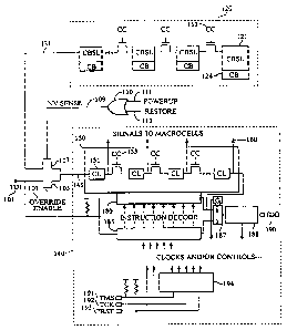
Referring to Fig. 1, the JTAG interface,
commonly known as a Boundary-Scan test circuit, 140 is
used to provide data to a Configuration Register (CR)
150.
As explained previously, the basic architecture
of the boundary-scan test circuit 140 consists of an
Instruction Register 185, a Test Access Port (TAP)
controller 194, Test Data Registers 180 and a Test Access
Port. The Test Access Port consists of four or five pins
on the IC package that are dedicated to Boundary Scan and
are not shared with any other functions. These pins are
used with a simple protocol to communicate with on-chip
Boundary-Scan logic. The protocol is driven by two of
the pins, Test Clock (TCK) 192 and Test Mode Select (TMS)
191. (The protocol is also driven by a third pin, if the
optional Test Reset (TRST) 193 pin is used.) The remain-
ing two pins of the Test Access Port are for serially
shifting data into and out of the IC, these pins being
called Test Data In (TDI) 101 and Test Data Out (TDO)
190. The TAP controller 194 is a simple finite state
machine with 16 states located on the IC die. The TAP
controller 194 recognizes the communication protocol and
generates internal control signals used by the remainder
of the Boundary Scan logic. The TAP controller 194 is
CA 02295445 1999-12-20
WO 99/54839 -7- PCT/US99/06355
driven by the signals of the TCK 192 and TMS 191 (and
optionally TRST 193) test pins.
The Instruction Register 185 is controlled by
the TAP controller 194 and can be placed between TDI 101
and TDO 190 for loading (and unloading) with serially
shifted data. The Instruction Register 185 is used to
set the mode of operation for one or more test data
registers 180. (The instruction modes and rules for
adding user-defined instructions are described in the
above referenced IEEE Standard 1149.1.) Each Instruction
Register cell comprises a shift register flip-flop and a
parallel output latch. The shift registers hold the
instruction bits moving through the instruction register.
The latches hold the current instruction. The minimum
size of the Instruction Register is two cells. The size
of the register dictates the size of the instruction code
that can be used, as the code size must match the length
of the register.
The test data registers 18o are placed between
the TDI pin 101 and the TDO pin 190. Two test data
registers are always required to be present on JTAG
component, the Bypass Register and the Boundary Register.
The Boundary Register is used to control and observe
activities on the ICs input and output pins. The Bypass
Register shortens the scan chain to a single cell, which
is useful when testing other boundary-scan components on
a board. Additional test data registers are optional.
The test data is shifted through the test data register
180 to a multiplexer 187, and then through an output
buffer 188 to the TDO pin 190. For complete details, one
may refer to the above referenced IEEE Standard 1149.1,
IEEE Standard Test Access Port and Boundary-Scan Archi-
tecture.
In the present invention, the CR 150 is in-
eluded within the JTAG structure as a test data register
180. Each bit in the CR 150 consists of a configuration
latch (CL} 151. Each CL 151 has an output that is used
as a configuration control signal 160 within a macrocell.
CA 02295445 1999-12-20
WO 99/54839 -g- PCT/US99/06355
The input data signal 149 for the CR 150 is selectably
provided from either a set of serially connected configu-
ration bit non-volatile element's sense latches 120 or
from the JTAG Test Data In (TDI) data pin 101 that is
used for reconfiguration and testing.
The system is initiated upon an initial power-
up signal 111 which is processed through an OR gate 110
to produce the non-volatile elements' sensing signal (NV
sense signal) 109. Upon initial power-up, the states of
the non-volatile elements are sensed in parallel and are
stored in the Configuration Bit sense latches (CBSL) 120
(shown as a series of individual CB sense latches, 121,
and synchronized by a Configuration Clock (CC) 153.) The
NV sense signal 109 is processed to the gate of FET 107,
which switches on the FET 107, thus processing the Sense
Latch Output Signal 131 through the FET 107 to the
Configuration Register input 149. The Configuration
Clock (CC) 153 is toggled for K clock cycles, where K is
the Configuration Register length in bits. In this
manner, the non-volatile elements data, which was stored
in the Configuration Bit Sense latches 120, is loaded
into the Configuration Register 150 upon power-up. Due
to the speed of the latches, this process is very fast.
After the power-up stage, testing may be
initiated by activating the Override Enable Signal 103 to
the gate of FET 105. This enables the JTAG TDI data
input pin 101 to be used as the CR data input 149. (It
is noted that the override enable signal 103 should be
used after the power-up stage has been completed, so as
to avoid the situation where a power-up signal is sent to
the FET 107 at the same time as the override enable
signal 103 is sent to FET 105, which would cause con-
flicting signals to occur.) The JTAG TDI data input pin
101 can then be used to process test configuration bits
into the configuration register 150 in order to carry out
the testing. Since the standard JTAG test specification
is used, standard industry test methods may be used.
(Again, one may refer to IEEE Standard 1149.1, IEEE
CA 02295445 1999-12-20
WO 99/54839 PCT/US99/06355
-g-
Standard Test Access Port and Boundary-Scan Architecture,
for more detail on how the testing is implemented.)
After the testing has been completed, the
Restore signal 113 may be used to initiate the same
configuration load sequence performed during power-up.
This provides a way to set the configuration latch states
to those stored in the configuration bit s non-volatile
elements without having to change the power supply level.
One of the advantages of the present invention
is that one can serially load different configurations
into the output macrocells without having to erase and
reprogram the non-volatile elements. Thus, this process
is much faster than other processes in which the non-
volatile elements have to be erased and reprogrammed.
Having to erase and reprogram the non-volatile elements
takes considerable test time as, after erasing and
reprogramming, the configuration bits need to be reloaded
to check the functionality of the macrocells. Addition-
ally, this system avoids the problems associated with
multiple erasures of the non-volatile elements, such as
excessive wear due to breakdown of the dielectric mate-
rial. This process can also be used for prototyping of
the integrated circuit chips.
An alternative embodiment of this invention is
shown in Fig. 2. In this embodiment, the need for using
Configuration Bit Latches is eliminated by parallel data
connection of the individual configuration bit non-
volatile elements (CB) 221 to configuration register
bits. Fig. 2 shows the portion of the circuit relating
to the configuration register 220. It is assumed that
the configuration register 220 is a Test Data Register as
defined in the JTAG test structure (and explained in
Fig. 1) .
Upon initiation by the Power-up Signal 211, the
NV sense signal 209 is sent to the gates of the FETS 205
to load the configuration bit non-volatile elements (CB)
221 to the Configuration latches (CL) 230. The outputs
of the CL 230 are used as configuration control signals
CA 02295445 1999-12-20
WO 99/54839 -10- PCT/l1S99/06355
260 within a macrocell. The Override Enable Signal 203
can be subsequently used to activate testing, and test
configuration bits can be loaded through the TDI test pin
201. The test configuration bits are tested through the
configuration latch portion of the circuit 230 in accor-
dance with JTAG specs and exit the configuration register
220 via a connection that leads to the TDO (Test Data
Output) 290. After testing, the Restore Signal 213 can
be used to reload the configuration latches 230. As
discussed, this embodiment eliminates the need for the
configuration bit sense latches. However, the configura-
tion bits 221 are required to be physically located near
the configuration latches 230 in order to avoid having to
route each CB output over a long distance.
Other circuitry may be added to the two embodi-
ments of this invention described above in order to
perform additional functions. For example, as shown in
Fig. 3, the configuration latches 33o and the configura-
tion bit non-volatile elements 321 can be logically
combined (using AND gates 380 and OR gates 390) within
the Configuration Register 320 to produce the configura-
tion control signals 360 to the macrocell.
Additionally, this invention s method for
controlling programmable bits may be used for other
purposes other than controlling bits within a macrocell.
These other purposes could include controlling pinout
control options, security bits, global logic configura-
tion control bits or speed/power options.
Also, it is possible to apply a control signal
to the configuration bits or to the configuration latches
in order to hold the configuration control signals in a
fixed state during the time that data is being input to
the configuration latches or while the configuration bits
are being programmed or erased.
Finally, it is anticipated that multiple
configuration registers can be connected in parallel
within the structure described above in order to process
multiple configuration bits at one time.
*rB