Note: Descriptions are shown in the official language in which they were submitted.
CA 02295541 2000-O1-06
WO 98/53651 PCT/US98/10525
1
A SYSTEM AND METHOD FOR PACKAGING
INTEGRATED CIRCUITS
CROSS REFERENCE TO RELATED APPLICATIONS
This application is a nonprovisional application of U.S. provisional
patent application "A SYSTEM AND METHOD FOR PACKAGING INTEGRATED
CIRCUITS," U.S. Serial Number 60/047,531, filed May 23, 1997, having Sammy
K. Brown, George E. Avery, and Andrew K. Wiggin, Tom L. Todd and Sam Beal
listed as co-inventors and assigned to Alpine Microsystems. The 60/047,531
application is hereby incorporated by reference in its entirety.
BACKGROUND OF THE INVENTION
The present invention relates to the packaging of semiconductor
devices, and more particularly to a system and method for interconnecting
integrated
circuits (ICs) on a semiconductor substrate.
Electronic systems typically are manufactured from two or more ICs to
provide complete system function. Until recently the limitations on
performance and
number of I/O pins were not significant for the vast majority of applications.
However, as more devices are integrated in a single IC and as clock speeds
increase,
limitations on performance and number of I/O pins would be of paramount
concern to
semiconductor manufacturers. This is because the overall performance of the
system
is based on multiple ICs is a function of the performance of the individual
ICs and of
the performance of the signals between the ICs. The performance of the signals
between the ICs is in turn a function of the number of signals and the
electrical
characteristics of the means used to connect the I/O pins of the ICs. A more
efficient
means for interconnecting ICs is therefore becoming an important influence on
the
cost, size, performance, weight, and efficiency of electronic systems.
CA 02295541 2000-O1-06
WO 98/53651 PCT/US98/10525
2
Currently, the most common method used for interconnecting ICs is to
first package the individual ICs, and then mount the packaged ICs on a
substrate such
as a printed circuit board. The size of the package is typically several times
larger
than the IC and is often manufactured from a metal lead frame and protected
within a
S plastic molded case. The packaged ICs are then placed and soldered to a
printed
circuit board to create a complete electronic system. The advantages of the
current
method include low cost and protection of the IC during subsequent handling.
In
addition, the package acts as a standardized carrier for testing of the IC,
such that
design changes to the printed circuit board may be made cheaply and quickly.
Assembly of the IC to the printed circuit board may further be automated.
Finally,
the current system allows rework of the printed circuit.
A more efficient method is necessary, however, as advanced ICs
require higher performance and larger number of I/O pins than is possible with
conventional interconnect technology. The conventional method has limited
electrical
performance and limited ability to remove heat. The electrical parasitic
characteristics of the package, the length of conductors, the electrical
parasitic
introduced by the structures of the printed circuit board, and the dielectric
material
used in the printed circuit board all limit the electrical performance of the
method.
These limitations in turn limit the number of signals on the system to at most
a few
hundred regardless of the complexity of the IC or the system. Since the
current IC
interconnection has lower performance than the ICs, it limits the overall
system
performance.
Integrated circuits are performing at above 100 MHz. The current
method of interconnecting ICs is, however, limited to systems operating below
100
MHz. An efficient means of interconnecting integrated circuits is therefore
necessary
to keep pace with corresponding advances in integrated circuit performance.
SUMMARY OF THE INVENTION
The present invention provides a system and method for efficiently
interconnecting a plurality of ICs, thereby improving the electrical
performance of the
overall system.
_.... _v_w.. .. . . _ ...._.._T...
CA 02295541 2000-O1-06
WO 98/53651 PCT/US98/10525
3
In one embodiment of the system of the present invention, a plurality
of carriers corresponds to a plurality of ICs, and a board has a plurality of
board
regions for receiving the plurality of ICs. Each carrier has first and second
sets of
contacts, and a set of interconnects therebetween. The first set of contacts
connects to
contacts on the corresponding IC when the corresponding IC is mounted to the
carrier's surface. Each board region has a set of board contacts connecting to
the
respective carrier's second set of contacts, and the board has a set of board
interconnects connecting selected contacts of the set of board contacts. The
plurality
of board regions are further formed with an opening sized to clear the
respective
carrier's IC when the respective carrier is mounted to the board.
In one embodiment of the method of the present invention, a plurality
of ICs is mounted to corresponding carriers. Each corresponding carrier has a
surface with sufficient contacts, and a set of contacts on the carrier is
routed to a set
of contacts on the IC using embedded interconnects. A board having openings is
provided, and the ICs are fitted into openings in the board with the carriers
engaging
the board.
These and other embodiments of the present invention, along with
many of its advantages and features, are described in more detail in the text
below
and the attached figures. In the figures, like reference numerals indicate
identical or
functionally similar elements.
BRIEF DESCRIPTION OF THE DRAWINGS
Fig. 1 shows an exploded view of the different components for
efficient interconnection of ICs according to the system of the present
invention;
Figs. 2A-2C show a tap view of the IC/carrier subassembly on the
board, a side view of the IC/carrier subassembly, and a side view of the
IC/carrier
subassembly on the board, respectively;
Fig. 3 shows an example set of electrical interconnections on a
carrier;
Fig. 4 is cross sectional view of the carrier shown above in Fig. 3;
Figs. 5A-SB show a single IC mounted on a carrier, and multiple ICs
mounted on a carrier, respectively;
CA 02295541 2000-O1-06
WO 98/53651 PCT/US98/10525
4
Fig. 6 shows the steps for interconnecting ICs efficiently according to
the method of the present invention;
Fig. 7 shows the steps of a method for interconnecting ICs according
to an alternate method of the present invention;
Fig. 8 is a simplified plan view of a carrier wafer in accord to the
present invention;
Fig. 9 is a detailed plan view of a portion of the carrier wafer shown in
Fig. 8;
Fig. 10 is a perspective view of a microrack assembly;
Fig. 11 is a perspective view of a microrack assembly in accordance
with an alternative embodiment; and
Fig. 12 is a perspective view of a microrack assembly in accordance
with a second alternative embodiment.
DESCRIPTION OF THE PREFERRED EMBODIMENT
The present invention provides a system and a method for efficient
interconnection of ICs to form a complex electronic component with improved
overall
system performance.
Fig. 1 shows an exploded view of an integrated circuit {IC) 10
mounted to a carrier 12, and a board 14 with a plurality of openings 16. As
shown,
board 14 has four openings 16, however, the number of openings 16 changes
according to the number of carriers to be connected to board 14. Similarly,
though
openings 16 are shown to be of equal sizes, they may differ in size in another
example as the sizes of the openings are determined by the sizes of the ICs to
be
electrically connected to board 14. In the example as shown in Fig. 1, carrier
12 is
connected to IC 10 only. However, as later discussed, carrier 12 may be
connected
to more than one IC or to other electronic components. If carrier 12 is
connected to
only one IC, the number of carriers for the system will depend on the number
of ICs
in the complex IC. In a preferred embodiment, the sizes of the carriers
correspond to
the sizes of the ICs in the complex IC, and the size of the board corresponds
to the
size of the complex IC.
CA 02295541 2000-O1-06
WO 98/53651 PCT/US98/10525
S
Carrier 12 is preferably thermally compatible with board 14 and IC I0,
since carrier 12 connects IC 10 and board 14. Thermal expansion compensation
between IC 10, carrier 12, and board I4 may be accomplished by the use of
compliant materials such as wires to make connections between the IC and the
package. Alternatively, bonding materials may be used to limit the stresses.
The
preferred method, however, is to have carrier 12 and board 14 be made of
materials
with similar Coefficient of Thermal Expansion (CTE) as IC 10. In a preferred
embodiment, carrier 12 and board 14 are made of the same material as IC 10.
Since
ICs are typically manufactured from single crystal silicon, which has a
relatively low
CTE, silicon is the preferred carrier and board material. However, gallium
arsenide
or other materials with comparable CTE may also be utilized.
Fig. I also shows the interconnections on board 14. Board 14 is
manufactured employing semiconductor photo lithographic processes; hence, the
routing density of board interconnections 20 on board 14 is higher than that
for
conventional board level interconnect. Connections 22 on carrier 12 are pre-
manufactured to fit the bond pad pattern of connections 24 on board 14. Board
14,
therefore, serves both as a mechanical base and implements at least a single
layer of
routing through interconnections 20 between neighboring carriers and ICs.
There are
preferably no vias in board 14 as the IC interconnections are preferably
distributed
among the carriers by allowing signals between the ICs to be passed through
neighboring chips. Since all subsystem routing is preferably distributed
across the
individual carriers, the complexity of the board routing is reduced to single
node sets.
Compared to a single interconnection board, interconnection distributions
among the
carriers greatly simplify the interconnection task, and significantly improve
the
overall system performance. Although board 14 preferably has only one level of
interconnect, in applications where yield is not critical, board I4 could have
multiple
levels of interconnect. In such applications, there would be vias in board 14
as the
interconnections would include pass-throughs as well as crossovers.
Figs. 2A-2C show a top view of an IC/carrier subassembly 25 on
board 14, a side view of IC/carrier subassembly 25, and a side view of
IC/carrier
subassembly 25 on board 14, respectively. As shown in Fig. 2B, subassembly 25
consists of IC 10 mounted to carrier 12. Carrier 12 is pre-manufactured with
solder
CA 02295541 2000-O1-06
WO 98/53651 PCT/US98/10525
6
bumps (shown as connections 21 and 22) which are placed in arrays aligned to
mirror
the bond pad patterns of IC 10 and board 14, respectively. IC 10 is flip chip
bonded
to carrier 12 through connections 21. As shown in Fig. 2C, each subassembly 25
is
mounted to board 14 so that IC 10 will fit within opening 16. As can be seen,
carrier
12 extends around opening 16 and connects to board 14 through connections 22.
Typically, the number of connections 21 between IC 10 and carrier 12 will not
be
equal to the number of connections 22 between carrier 12 and board 14.
The use of opening 16 enables all of the signal connections to lie in a
plane formed by the top side of IC 10, the top side of carrier 12, and the top
side of
board 14. This configuration is very advantageous, as the chemical properties
of
silicon are such that it is impractical to form plated vias through silicon
materials
thicker than a few tenth of a micron. By using the same materials for carrier
12 and
board 14, direct solder connections may be made between carrier 12 and board
14.
Since IC 10 and carrier 12 are preferably made of the same materials, signal
connections may also be directly soldered on the carrier and connected to the
IC. As
previously discussed, the solder bumps on carrier 12 are aligned to minor IC
10's
bond pad pattern. Hence, IC 10 need not be solder bumped.
The advantage of using solder bumps to connect the IC to the carrier,
and the carrier to the board is that an area array may be used to maximize the
number
of external signal connections available. In addition, parasitics associated
with wire
bonding may be eliminated. Solder bump flip chip bonding is an automated
process,
and bumping cost does not increase with pin count. Hence, the use of solder
bumps
also enables integration of higher I/O pin counts while keeping cost low.
Fig. 3 shows an exemplary electrical interconnection configuration on
carrier 12. For simplicity, a relatively small number of connections are
shown. As
can be seen, carrier 12 has connections 22 along its peripherals and
connections 21
around its central portion. Connections 21 and 22 connect IC 10 to carrier 12,
and
carrier 12 to board 14, respectively. Connections 21 may be routed to
connections 22
using embedded interconnects, and such routing may have at least one
crossover.
These crossovers allow signals to be passed to and from the IC on carrier 12.
In
addition, the signal paths on carrier 12 may be independent of the IC routing.
These
independent signal paths serve as pass throughs for signals from a neighbor IC
to
.... .. ....._. "_..,._ _......... ... .~...... . ..... _.. .....
CA 02295541 2000-O1-06
WO 98/53651 PCT/US98/10525
7
other neighboring ICs. In this manner, interconnection of the ICs are
distributed
across the individual carriers.
Connections 21 and 22 are predetermined according to the application
of the particular complex ICs. Since connections 21 and 22 are manufactured
using
semiconductor photolithography techniques, the resulting routing density is
very
similar to the density of on-chip interconnect. Specifically, connections 21
and 22 are
made through inner and outer rows of solder bumps, deposited in patterns to
match
the bond pads of the IC 10 and the board 14. This eliminates the need to place
solder
bumps on individual ICs. The number of connections between ICs, known as
external interconnect, generally requires significantly less interconnect
density than
the interconnect density used to connect transistors on the IC. Hence, the
external
interconnection density can always be made high enough by using the same or
less
advanced semiconductor process that is used to fabricate the IC itself. Using
this
same technique, the external interconnections may also be made to fit into an
area that
is the same or less than the area of the IC itself. This provides a
significant yield
advantage over the current method as the size and area of printed circuit
boards are
generally many times larger than the ICs themselves.
Referring to both Figs. 3 and 4, Carrier 12 is manufactured from a
mufti-level semiconductor metallization process. Crossovers between the signal
paths
are achieved through the use of vias, which are located within the same layer.
Since
all the vias are in the same layer, custom changes to connections 21 and 22
may be
made easily at the manufacturing level by single-mask programming. For each
new
application, the location of the vias may be determined according to the
particular IC
interconnections desired. Once the locations of the vias have been determined,
only
the via-containing layer needs to be changed.
The carrier 12 contains a multiple level interconnection matrix with at
least 800 signal paths /cm2. The configuration of the interconnection matrix
is mask
programmable and facilitates high-speed data signal propagation in excess of
20GHz.
The input and output (I/O) signals of the IC 10 can be routed to multiple
sides thereof
the die, effectively tripling the I/O density of the IC 10. The carrier 12
interconnection matrix is composed of two signal layers 12a and 12b sandwiched
between reference planes for power 12c and ground 12d. Each layer is 5
CA 02295541 2000-O1-06
WO 98/53651 PCT/US98/10525
8
micrometers of electroplated copper. The power layer 12c provides a reference
plane
for Vdd and includes a hiatus in which a bond pad connection 12e is disposed.
By
surrounding the two spaced-apart signal paths 12a and 12b between two power
planes
12c and 12d, the noise, such as crosstalk and simultaneous switching noise
(SSN), in
the signal paths 12a and 12b is reduced.
Crosstalk results from mutual capacitance between two adjacent signal
lines. For the carrier 12, the resulting crosstalk noise can be estimated as
follows:
V~~ = 0.176 x 10'9 (V;~'Trise)
where V;~ = input voltage. Far end crosstalk tends to cancel and can be
neglected.
SSN created in the Vop/Vss loops formed by the output buffer's discharge path
is
frequently called ground bounce since it is superimposed on the local ground
plane
12d (applies to the power plane 12c, as well). The magnitude of the noise
voltage
can be approximated as follows:
VSS" - I'eff dI/dt
where Leff 1S the effective self inductance of the die to package to ground
connections.
The equation tends to overestimate VSS~ bY neglecting negative feedback
effects dI/dT.
The circuit noise margins must be sufficient to guarantee proper operation in
the
presence of SSN. The flip-chip attachment process used for the carrier 12 and
the
board 14 assembly offers extremely low ( < O.1nH) parasitic inductance, and
the
carrier 12 contains non-perforated reference planes.
By surrounding the two spaced-apart signal paths 12a and 12b between
two power planes 12c and I2d, the distance between each of the power planes
12c
and 12d and the signal paths 12a 12b may be easily controlled so as to be
constant
over the volume of the carrier. This facilitates formation of a constant
impedance
between power plane 12c and signal path 12a, as well as power plane 12d and
signal
path 12b. In addition, the crosstalk is avoided by placing signal path 12a
proximate
to power plane 12c and signal path 12b proximate to power plane 12d. In this
fashion, the return path for the current in the signal propagating along one
of the
. .....__.._ _._. . _.
CA 02295541 2000-O1-06
WO 98/53651 PCT/US98/10525
9
paths 12a or 12b is not the signal path adjacent thereto, but rather the power
plane
12c or 12d.
Noise may be further reduced by abrogating reflection noise, which is
caused by an impedance mismatch between a driver and receiver. Reflection
noise
becomes problematic when the time of flight of a signal is comparable with the
signal's rise time. Consequently, very short connections that satisfy the
following
constraint will minimize reflection noise problems.
't7ight < trise~4'
For a typical carrier 12 signal interconnect, the time of flight is:
flight - SOpS.
Hence, by keeping rise and fall times > 200ps, reflection noise and the
resulting
impact on settling time can be avoided. For 3.3V transitions, this translates
into an
interconnect load capacitance of < 66pF per interconnect. In this fashion, the
carrier
12 provides a high-density routing structure with low noise by which to
interconnect
various pads of a single IC 10, or multiple ICs 10.
The board 14, on the other hand, serves as a mechanical base for the
carrier 12 while providing single-layer routing between adjacent carriers 12.
The
combination of mufti-layer carrier 12 interconnection matrix and the single-
layer
signal path of the board 14 interconnect effectively produces a continuous
connect X
Y interconnect plane over the mufti-chip subsystem. Carriers 12 that do not
have
direct connections to a board 14 adjacent thereto shares a power plane 12 c or
12d
with another carrier 12. Although it is not necessary, it is preferred that
carriers
and/or ICs 10 that are to be in data communication, i.e., electrically
coupled, should
be positioned proximate to each other.
In addition to providing adequate current-carrying paths for the total
peak requirements of the individual IC 10, the carrier 12 and board 14
combination
must provide sufficient power dissipation to satisfy the estimated power
consumption
of the device. In an effort to improve the power characteristics of the
carrier 12
board 14 combination, it is preferred that the IC 10 employ low-swing signal
techniques.
Fig. SA shows a single IC 10 mounted on carrier 12. As shown in
Fig. 5B, multiple ICs may also be mounted on carrier 12. Although Figs. SA and
SB
CA 02295541 2000-O1-06
WO 98/53651 I'CT/US98/10525
show only ICs on carrier 12, resistors, capacitors, and other electrical
components
may be mounted on carrier 12 along with the ICs. Hence, carrier 12 functions
as a
mufti-chip module within itself. This is very advantageous as more components
may
be interconnected on board 14. Moreover, with carrier 12 as an intermediate
board,
5 the interconnections are comparable to on-chip interconnects.
The process for fabricating the carrier 12 using a batch process
includes employs conventional chemical vapor deposition techniques. In one
example
a wafer is prepared for processing by removing native oxide therefrom.
Thereafter,
the wafer surface is nucleated with a layer of copper approximately 4,000
angstroms
10 thick. The copper layer is deposited to have a substantially even thickness
over the
surface of the wafer. A layer of photoresist is deposited over the nucleations
layer to
a thickness in the range of 8 to 10 microns. The layer of photoresist is used
as a
plating barrier to form the power planes 12a and 12b, shown above in Fig. 4.
The
power planes 12a and 12b are defined by a mask layer which is deposited atop
of the
photoresist. Thereafter, a photoresist anisotropic etch step removes the
photoresist
from the regions defined by the mask, exposing the nucleation layer. A layer
of
copper 5.0 microns thick is disposed in the regions removed by the
aforementioned
etch step using electroplating techniques. Specifically, the periphery of the
wafer is
attached to a plating electrode to allow contact between the electrode and the
nucleation layer. The wafer is then immersed in a copper electroplating bath
where
approximately 5 microns of copper are plated into the aforementioned regions.
After
completion of the electroplating step, the photoresist is removed leaving the
patterned
power planes 12a and 12b. The copper nucleation layer remains shorting all
metal
patterns present on the wafer.
A blanket wet etch is then performed to remove the copper nucleation
layer and provide electrical isolation between power planes 12a and 12b. An
adhesion promoter, 3-Aminopropyltriethoxysilane (3-APS), 0.5 % in methanol, is
used disposed on the wafer. The 3-APS solution is dynamically dispensed onto
the
center of the wafer while the wafer spins at 3000 rpm. The spin speed is then
increased to 5000 rpm for 30 seconds to dry the surface. Thereafter, a
dielectric
layer of BCB is deposited. The dielectric layer has a thickness of
approximately
_..__..... . ........ ....... ....,...
CA 02295541 2000-O1-06
WO 98/53651 PCT/US98/10525
11
5.0 microns and electrically insulates power planes 12a and 12b, forming a
microstrip
transmission line structure. The 3-APS enhances the adhesion of BCB to copper.
A second mask is disposed atop of the dielectric layer to position and
define vias, which are subsequently etched during a Photo-BCB develop process.
This is followed by the sputtering of a 4,000 angstrom thick TiCu which covers
the
entire wafer. The TiCu layer functions as a plating electrode for a subsequent
copper
electroplating step. The electrode attachment is on the outer edge of the
wafer. A
second layer of photoresist approximately 8 to 10 microns thick is deposited.
The
second photoresist is used as a plating barrier to form the one of the signal
layers I2c
and 12d, which is defined by a mask. The photoresist is then anisotropically
etched,
exposing the TiCu layer in various regions of the photoresist. Copper, up to
five
microns thick is deposited in the aforementioned vias, as well as the regions
exposed
during the anisotropic etch using an electroplating technique. The photoresist
is then
removed leaving the signal paths 12c and 12d formed by an additive process. A
blanket wet etch is now performed to remove the TiCu layer and provide
electrical
isolation between signal layers 12c and 12d. Another layer of 3-APS adhesion
promoter and BCB is then deposited. The layer of BCB is approximately 2.0
microns
thick.
A fourth mask is applied to define the interconnections 21 and 22,
followed by an etch which removes portions of the BCB layer. A nickel and gold
plating is performed in the aforementioned portions. A fifth mask is applied
to define
the regions where segments of the BCB layer is removed, exposing regions of
the
silicon wafer. A dry etch is then used to remove the segments of the BCB
layer. A
layer of 3-APS adhesion promoter is now applied to the side of the wafer
opposite to
the side where the fifth mask was deposited, and a 2 micron thick layer of BCB
is
deposited thereon, defining a backside BCB layer. A sixth mask is disposed on
the
backside BCB layer and defines regions where the silicon wafer is to be
exposed. A
dry etch is used to expose the wafer silicon. followed by removal of the
silicon from
these regions. The backside BCB layer is then removed. The board 14 is made in
an
analogous manner.
Fig. 6 is a flowchart showing the preferred method of interconnecting
ICs according to the present invention. As shown, for each complex IC, the
board
CA 02295541 2000-O1-06
WO 98/53651 PCT/US98/10525
12
wafers, the carrier wafers, and the IC wafers are separately manufactured.
Referring
to step 501, after the board wafers are fabricated, openings are formed in the
boards
at step 503. The individual boards are separated at step 505, and tested at
step 507.
The carriers are fabricated at step 521, and are tested and sorted for
defective units at
step 523. Defective units are discarded, and the good units are separated into
individual carriers at step 525. Referring to steps 541 through 545, the ICs
are also
tested for defects once they are fabricated. The good units are also sorted
from the
defective units and are separated into individual ICs. At step 550, the good
IC dies
are mounted onto corresponding good carriers. After the ICs have been mounted
to
the carriers, a final test of the IC is conducted at step 555. This additional
test before
the IC is integrated with other subsystem ICs eliminates the burden of
producing
"known good die. " Since no assumptions are made regarding the quality of the
die,
compound yield loss is also eliminated. The IC/carrier subassembly is mounted
onto
the board at step 570. Bad connections are tested for at step 572, and upon
passing
the test, the assembly is completed at step 574.
Referring to Figs. 7 and 8, an alternative method of interconnecting
ICs according to the present invention is shown. Specifically, steps 601, 603,
605
and 607 correspond to steps 501, 503, 505 and 507, discussed above with
respect to
Fig. 6. The method shown in Fig. 7, however, differs in that the individual
ICs 110
are assembled onto the carriers (not shown) before the carriers are segmented.
Specifically, the carrier wafer 112a is fabricated at step 621 so as to have a
plurality
of spaced-apart carrier regions 112 located therein. In a separate process,
ICs 110
are fabricated at step 641. Thereafter, the ICs 110 are segmented at step 645
and
assembled onto the carrier wafer 112a at step 647, using the solder attach
techniques
discussed above. In this fashion, each carrier region 112 will have at least
one IC
110 associated therewith.
Referring to Figs. 3, 7 and 8, attachment of the ICs 110 before
segmentation of the carriers 12 allows performing 100 % functional testing or
burn-in
of the ICs I10, before final assembly. To that end, the carrier wafer 112a
includes a
power plane 120 and a ground plane 122, as well as signal paths 124. Each of
the
carrier regions 112 may be coupled to the power plane 120 and the ground plane
122
through interconnects 126. In this configuration, ICs 110, associated with the
carrier
~_ _ _ _ _rv.._.
CA 02295541 2000-O1-06
WO 98/53651 PCT/US98/10525
13
regions 112, may be tested before completing assembly at step 570.
Specifically, the
signal paths 124, the ground and power planes 120 and 122 and the
interconnects 126
are in electrical communication with the requisite connections 21 to
facilitate biasing
and signal transmission to the ICs 110. Thus, early detection of defective ICs
I10
may be achieved. The carrier region 112 and IC 110 may be discarded after
segmentation, but before final subassembly into a board 14, thereby saving the
cost of
disposing of a properly functioning board 14. In addition, reduced is the
probability
that damage to the IC I10 will occur during functional testing, because
coupling of
the test signals and bias voltages to the ICs 110 occurs at coupling pads 124a
and
126a. There is no physical contact with the IC 110 and the testing unit (not
shown)
during burn-in.
Referring to Figs. 8 and 9, the signal paths 124 and interconnects 126
are routed to each of the carrier regions 112 by passing through test
circuitry regions
130, located between adjacent carrier regions 112. Also included in the test
circuitry
regions 130 are other circuit elements necessary to properly configure the ICs
located
in the carrier regions 112 for functional testing. For example, isolation
resistors 132
and 134 may be disposed therein. In this fashion, each IC 110 may be coupled
to the
power plane 120 and ground plane 122 via isolation resistors 132 and 134,
respectively. This prevents a short associated with one of the carrier regions
112,
from shorting the entire carrier wafer 112a. During the segmentation step 670,
shown in Fig. 7, the test circuit regions 130 and the power and ground planes
120
and 122, shown in Fig. 9, are bisected. This allows segmentation of the
carrier wafer
112a without damaging the individual carrier regions 112. Bad connections are
tested
for at step 672, and upon passing the test, the assembly is completed at step
674,
shown in Fig. 7.
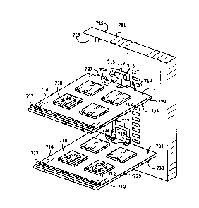
Referring to Fig. 10, the overall bandwidth among the ICs 710 within a
system is a major determinant of the performance of an electronics system,
with the
external performance of the ICs 710 being equal to the interconnect routing
density
times the frequency bandwidth between I/O pins. To further increase the
density of
the integrated circuits, in a unit volume, and the performance thereof, a
backplane
711 is provided so that the individual boards 714 may be coupled thereto
thereby
extending the 2-D board 714 into a 3-D subassembly. As discussed above, the
board
CA 02295541 2000-O1-06
WO 98/53651 PCT/US98/10525
14
714 may have a carrier 712 with an integrated circuit 710 mounted thereto. The
backplane 711 includes a plurality of bond pads 715 and a plurality of signal
paths
717, with a subset of the plurality of bond pads tying on a first major
surface 723 of
the backplane 711. At least one through-way 719 is formed into the backplane
711
and extends, from an aperture 721 formed into the first major surface 723,
toward an
opposing major surface 725.
When extending the 2-D board 714 into a 3-D subassembly, it is
desirable to as match as closely as possible the I/O bandwidth among the
boards 714 to
the bandwidth within the boards 714. This implies a high interconnect routing
density
between boards 714, requiring some form of structure move the signals between
the
planes of the 2-D boards 714. As a result, the complexity of a 3-D subassembly
is
approximately equal to the complexity of its constituent boards 714 times the
number
of the same. For example, in a subassembly having ten boards 714, the overall
system
level complexity is 10X. To interconnect the boards 714 and the backplane 71
I,
precise control of the manufacturing tolerances of the same is necessitated.
To that end,
the backplane 711 is formed in a manner described above, with respect to the
formation of boards 714. This allows establishing the mechanical tolerances of
the
various features of the subassembly using photolithography and etching
techniques.
Specifically, the crystalline structure of silicone allows precise etching of
the board 714
and backplane 711. In this fashion, mechanical tolerances of I micron can be
formed
by the etching process. Assuming a worst case misalignment accuracy of 20%,
pad
pitches of S micron could be built. Therefore, the tolerances between the
electrical
connections and the mechanical structure may be set by the accuracy of the
photo
alignment equipment.
To facilitate accurate coupling of the boards 714 to the backplane 711,
each board includes at least one tenon 727, one end of which has a cross-
section
complementary to a cross-section of the through-way 719. Although the tenon
727
may be formed so as to extend from any surface of the board 714, preferably at
least
one tenon 727 extends from a periphery 729 of the board 714 that lies in a
plane
orthogonal to the plane in which the opposed major surfaces 731 and 733 of the
board
714 lie. In this fashion, upon reaching a final seating position, with respect
to the
backplane 711, the opposed major surfaces 731 and 733 of the board 714 lie in
planes
T T
......_ ~ . . __.
CA 02295541 2000-O1-06
WO 98/53651 PCT/US98/10525
that extend transversely to the planes in which opposed major surfaces 723 and
725
lie. In this final seating position, at least one of the plurality of bond
pads 715 is
positioned adjacent to one of the plurality bond pad pattern connections 724
on the
board 714.
5 To fixedly position the board 714 with respect to the backplane 711, it
is preferred to solder the bond pad 715 to a bond pad pattern connection 724
positioned adjacent thereto, defining a joint 735. To that end, the bond pads
715 and
the bond pad pattern connections 724 must include a material which wettable by
solder. Typically, the bond pads 715 and the bond pad pattern connections 724
are
10 plated with gold or nickel. The solder may be flowed employing any
technique
known in the art. Preferably, however, the solder is flowed employing a
localized
heating technique such as infra-red. In this manner, solder may be flowed
without
subjecting areas surrounding the solder to excessive heat. Typically, the
distance
between adjacent boards 714 is a function of the worst case tolerance which
15 determines the size of the throughway 719 relative to the tenon 727. The
height of
the pads on the board 714, the backplane 711 and the quantity of solder
employed
must be sufficient to ensure that there are no voids in the joint 715.
An advantage with employing solder is that it facilitates rework by
allowing replacement of a defective board 714 or integrated circuit 710
present
thereon. This is particularly important considering that the l OX increase
provided by
mounting ten boards 714 to a backplane 711 results in a l OX higher
probability of
system Level defects, compared to an individual board 714. With solder, rework
of the
subassembly is facilitated by reflowing the solder to decouple a defective
board 714
from the backplane 711, shown more clearly at joints 837 in Fig. 11. Referring
again
to Fig. 10, during the rework process, the bond pads 715 and the bond pad
connections 724 may be cleaned in a manner similar to the rework procedures
for
flip-chip technology. The process used for final assembly may then be
repeated.
After final assembly, the 3-D subassembly can be placed in a protective
package and
connections to the next level made.
To relieve stress at the joint 735, a side of the boards 714 positioned
opposite to the joint 735 may include a stud 737 extending from one of the
major
CA 02295541 2000-O1-06
WO 98/53651 PCT/US98/10525
16
surfaces. The stud 737 has dimensions sufficient to contact an adjacent board
714
and reduces cantilevering of the boards about the joint 737.
Referring to Fig. 11, in another embodiment, cantilevering of the
board 814 about the joints 837 may be avoided by providing a second backplane
811b, which may be disposed opposite to the first backplane 811a or extend
transversely thereto. The second backplane 811b is similar to the first
backplane, but
the board 814 would include first and second sets of tenons 827a and 827b,
each of
which is to be uniquely associated with one of the first and second back
planes 811a
and 811b. An added benefit of having multiple backplanes is that shorter
signal paths
may be provided, thereby reducing the worst case path length between signals
on any
boards to the average of board width plus the backplane separation. This
reduces
parasitic capacitances and inductances while increasing the transmission speed
of
signal in the 3-D module.
Referring to Fig. 12 another embodiment to prevent cantilevering of
the boards 914 about the joints 915 includes having tenons 927 attached to the
backplane at differing distances from one of the opposed major surfaces 931
and 933
of the board 914. To that end, one or more of the tenons 927 may extend,
toward the
backplane 911, from one of the opposed major surfaces 931 and 933, with the
remaining tenons 929 extending from the periphery. In this fashion, the
cantilevering
of the boards 914 about the joints 915 is reduced due to the joints lying in
two
different planes.
1 _._.~_~__ ._.. .. .._ ~..