Note: Descriptions are shown in the official language in which they were submitted.
CA 02296028 2000-O1-10
WO 99103309 PCTIUS98/13632
AN ELECTRODE STRUCTURE FOR HIGH RESOLUTION
ORGANIC LIGHT-EMITTING DIODE DISPLAYS
AND METHOD FOR MAKING THE SAME
Cross Reference to Related Applications
This application relates to and claims priority on prior U.S. Provisional
Application Serial No. 60/052,352, filed on July 11, 1997.
Field of the Invention
The present invention relates to organic light-emitting devices, and in
particular,
to an electrode structure for a high-resolution organic light-emitting diode
("OLED")
display device.
to Background of the Invention
EL devices, which may be generally classified as organic or inorganic, are
well
known in the graphic display and imaging art. Among the benefits of organic EL
devices, such as organic light-emitting diodes, are high visibility due to
self emission, as
well as superior impact resistance, and ease of handling of the solid state
devices.
15 OLEDs may have practical application for television and graphic displays,
as well as in
digital printing applications.
An OLED is typically a laminate formed on a substrate such as soda-lime glass.
A light-emitting layer of a luminescent organic solid, as well as adjacent
semiconductor
layers, are sandwiched between a cathode and an anode. The semiconductor
layers may
20 be hole-injecting and electron-injecting layers. The light-emitting layer
may be selected
from any of a multitude of fluorescent organic solids. The light-emitting
layer may
consist of multiple sublayers.
SUBSTITUTE SHEET (RULE 26)
CA 02296028 2000-O1-10
WO 99/03309 _ PCT/US98113632
When a potential difference is applied across the cathode and anode, electrons
from the electron-injecting layer, and holes from the hole-injecting layer are
injected into
the light-emitting layer. They recombine, emitting light.
In a typical matrix-addressed OLED display, numerous OLEDs are formed on a
single substrate and arranged in groups in a regular grid pattern. Several
OLED groups
forming a column of the grid may share a common cathode, or cathode line.
Several
OLED groups forming a row of the grid may share a common anode, or anode Line.
The
individual OLEDs in a given group emit light when their cathode line and anode
line are
activated at the same time.
IO OLEDs have a number of beneficial characteristics. These include a low
activation voltage (about 5 volts), fast response when formed with a thin
light-emitting
layer, and high brightness in proportion to the injected electric current. By
changing the
kinds of organic solids making up the light-emitting layer, many different
colors of light
may be emitted, ranging from visible blue, to green, yellow, and red. OLEDs
are
currently the subject of aggressive investigative efforts.
An OLED may be designed to be viewed either from the "top" -- the face
opposite
the foundational substrate -- or from the "bottom", i.e., through the
substrate, from the
face opposite the light emitting layer. Whether the OLED is designed to emit
light
through the top or the bottom, the respective structure between the viewer and
the light
emitting material needs to be sufficiently transparent, or at least semi-
transparent, to the
emitted light. In many applications it is advantageous to employ an OLED
display
having topside light output. This permits the display to be built on top of a
silicon driver
chip for active matrix addressing.
It has been a continuing challenge to devise OLED display structures which
provide topside light output while minimizing light blockage and thereby
permitting a
high-resolution display. Transparent conductors deposited on top of organics,
at low
temperature, tend to be excessively resistive. This adversely affects the
response time of
the device or peak brightness. Various methods have been tried including
transparent
conductors (e.g., ITO and IZO) on thin metal.
2
SUBSTITUTE SHEET (RULE 26)
CA 02296028 2000-O1-10
WO 99103309 PCTNS98/13632
Accordingly, there is a need for a top electrode structure for an OLED which
permits high resolution displays to be fabricated with low line resistance and
topside light
output. The present invention meets these needs, and provides other benefits
as well.
Objects of the Invention
It is therefore an object of the present invention to provide an electrode
structure
for high resolution OLED displays.
It is another object of the present invention to provide a method for making a
topside electrode structure for high resolution OLED display.
It is another object of the present invention to provide an electrode
structure for
an OLED which has low line resistance.
It is a further object of the present invention to provide an electrode
structure for
an OLED having topside light output.
It is still another object of the present invention to provide an electrode
structure
for an OLED which permits an OLED display to be built on top of a silicon
driver chip
for active matrix addressing.
It is yet another object of the present invention to provide a top electrode
structure
for an OLED which is compatible with solvent or water-soluble OLED displays.
It is another object of the present invention to provide a process for making
a top
electrode structure for high-resolution OLED displays having low line
resistance.
It is yet another object of the present invention to provide a method for
making
a top electrode structure for a high resolution OLED display with topside
light output.
Additional objects and advantages of the invention are set forth, in part, in
the
description which follows, and, in part, will be apparent to one of ordinary
skill in the art
from the description and/or from the practice of the invention.
Summary of the Invention
In response to the foregoing challenges, applicants have developed an
innovative
top electrode structure for a high resolution organic light-emitting diode
display device,
SUBSTITUTE SHEET (RULE 26)
CA 02296028 2000-O1-10
WO 99/03309 _ PCT/US98/13632
and top electrode structure comprising a transparent electrode and conductive
ribs
disposed on the transparent electrode.
Applicants have also developed a top electrode structure for an OLED display
device, the OLED display device comprising a substrate, a bottom electrode
disposed on
the substrate, and an organic light-emitting material disposed on the bottom
electrode, the
top electrode structure comprising a first conductive barrier disposed on the
organic light-
emitting material, a transparent electrode disposed on the first conductive
barrier, a
second conductive barrier disposed on the transparent electrode and highly
conductive
ribs disposed on the second conductive barrier.
Further, applicants have developed a top electrode structure for an OLED
display
device, the top electrode structure comprising conductive ribs, and a
transparent electrode
disposed on the conductive ribs.
The novel top electrode structure of the invention provides top side light
output
and a low Line resistance and enables a high resolution display.
The present invention is directed to an organic light emitting diode device
comprising a substrate, a first conductor located on the substrate, an organic
light
emitting layer located on the first conductor, and a second conductor located
on the
organic light emitting layer. The improved device according to the present
invention
includes at least one of the first conductor and the second conductor
comprises a
transparent electrode layer, and at least one conductive rib disposed on the
transparent
electrode Layer.
The at least one conductive rib may formed from a highly conductive material.
The highly conductive material may be formed from at least one material
selected from
the group consisting of at least one material selected from the group
consisting of Mo,
Ti, TiSi2, W, Ta, AI and alloys of Mo, Ti, TiSiz, W, Ta, and Al.
The transparent electrode layer may comprise at least one material selected
from
the group consisting of InSnO, InZnO, and ZnO.
The at least one of the first conductor and the second conductor may further
include a first conductive barrier located between the transparent electrode
layer and the
4
SUBSTITUTE SHEET (RULE 26)
CA 02296028 2000-O1-10
WO 99/03309 PCTIUS98/13632
at least one conductive rib. The at least one of the first conductor and the
second
conductor may further include a second conductive barrier located between the
organic
light emitting layer and the transparent electrode.
According to an embodiment of the present invention, the second conductor may
include the transparent electrode layer, and the at least one conductive rib
disposed on the
transparent electrode layer. The second conductor may further include a first
conductive
barrier located between the transparent electrode layer and the at least one
conductive rib.
The second conductor may further include a second conductive barrier located
between
the organic light emitting layer and the transparent electrode. The device may
further
include an encapsulation layer formed on the transparent electrode layer and
the at least
one conductive rib. The encapsulation layer may be formed from a material
selected
from the group consisting of SiC, diamond-like carbon and parylene. The
material may
be deposited by PECVD.
The first conductor layer may be formed from at least one material selected
from
the group consisting of Al, Cu and alloys of A1 and Cu. The first conductor
layer may
further include an electron injection layer. The electron injection layer may
include an
injection material selected from the group consisting of alloys of Mg and Ag,
alloys of
Li and Al, LiF on Al, Sc on Al, and Sc203 on Al. The first conductor layer may
further
include a reflective layer.
According to another embodiment of the present invention, the first conductor
may comprise the transparent electrode layer, and the at least one conductive
rib disposed
on the transparent electrode layer. The first conductor may further include a
first
conductive barrier located between the transparent electrode layer and the at
least one
conductive rib. The first conductor may further include a second conductive
barrier
located between the organic light emitting layer and the transparent
electrode. The device
may further include an encapsulation layer formed on the second conductor
layer. The
encapsulation layer may be formed from a material selected from the group
consisting
of SiC, diamond-like carbon and parylene. The material may be deposited by
PECVD.
5
SUBSTITUTE SHEET (RULE 26)
CA 02296028 2000-O1-10
WO 99/03309 , PCT/US98/13632
The second conductor layer may be formed from at least one material selected
from the group consisting of Al, Cu and alloys of A1 and Cu. The second
conductor layer
may further include an electron injection layer. The electron injection layer
may include
an injection material selected from the group consisting of alloys of Mg and
Ag, alloys
of Li and Al, LiF on Al, Sc on Al, and Sc,03 on Al. The second conductor layer
may
further include a reflective layer.
The present invention is also directed to a display device. The display device
may
include at least one organic light emitting diode device. Each of the at least
one organic
light emitting diode device may comprise a substrate, a first conductor
located on the
substrate, an organic light emitting layer located on the first conductor, and
a
second conductor located on the organic light emitting layer. The at least one
of the first
conductor and the second conductor may comprise a transparent electrode layer,
and at
least one conductive rib disposed on the transparent electrode layer.
The device may include at least two organic light emitting diode devices,
wherein
the at least one of the first conductor and the second conductor are common to
at least
two of the organic light emitting diode devices.
It is to be understood that both the foregoing general description and the
following detailed description are exemplary and explanatory only, and are not
restrictive
ofthe invention as claimed. The accompanying drawings, which are incorporated
herein
by reference and which constitute a part of this specification, illustrate
certain
embodiments of the invention, and together with the detailed description serve
to explain
the principles of the present invention.
Brief Description of the Drawings
The invention will be described in conjunction with the following figures in
which like reference numerals designate like elements and wherein:
Fig. 1 is a cross sectional side view and elevation of a preferred embodiment
of
an OLED display device of the present invention;
Fig. 2 is a top plan form view of the display device of Fig. 1; and
6
SU8ST1TUTE SHEET (RULE 26)
CA 02296028 2000-O1-10
WO 99/03309 PCT/US98/13632
Fig. 3 is a cross-sectional side view and elevation of an alternate preferred
embodiment of an OLED display device of the present invention showing four
pixels.
' Detailed Description of the Preferred Embodiments
Reference will now be made in detail to a preferred embodiment of the present
invention, an example of which is illustrated in the accompanying drawings. A
preferred
embodiment of the present invention is shown in Fig. 1 as organic light-
emitting diode
display device 10.
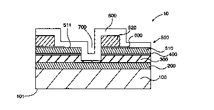
In a preferred embodiment, OLED display device 10 comprises a substrate 100,
a first conductor 200, an organic light-emitting stack 300, a first conductive
barrier 400,
a second conductor 500, a second conductive barrier 600, a channel 700 and an
encapsulation layer 800. The second conductor 500 includes a transparent
electrode 510
and at least one conductive rib 520.
As embodied herein, OLED display device 10 is a layered structure formed on
substrate 100. The first conductor 200 is disposed on the substrate 100, the
organic light-
emitting stack 300 is disposed on bottom conductor 200. The first conductive
barrier
layer 400 is disposed on organic light-emitting stack 300. The second
conductor 500 is
disposed on the first conductive barner layer 400. The second conductive
barrier layer
600 is disposed on transparent electrode 510. The at least one conductive rib
520 is
disposed on the second conductive barrier layer 600. Encapsulation layer 800
is
deposited on exposed surfaces of device 10.
It is contemplated by the present inventors that the device 10 can effectively
operate without either the first conductive barrier 400 and/or the second
conductive
barrier 600. When second conductive barrier layer 600 is not used, the at
least one
conductive rib 520 is disposed directly on transparent electrode 510. When
first
conductive barrier layer 400 is not used, the transparent electrode 510 is
disposed directly
on the organic light-emitting stack 300.
The at least one conductive rib 520 and the second conductive barrier 600
occupy
a small portion of surface 511 of transparent electrode 510. Surface 511
generally
7
SUBSTITUTE SHEET (RULE 26)
CA 02296028 2000-O1-10
WO 99/03309 _ PCT/US98I13632
defines the "top" of OLED display device 10, while surface 101 of substrate
100
generally defines the "bottom" of OLED display device 10. Channel 700 serves
as the
separation between adjacent diodes in the OLED display device 10.
The substrate 100 may be made of soda-lime glass. It is contemplated that the
substrate 100 is not limited to glass; rather, the substrate 100 may be formed
of silicon
or other suitable materials. For example, substrate 100 may comprise a silicon
driver
chip for active matrix addressing when OLED display device 10 is an active
matrix
addressed display.
First conductor 200 includes Al. The present invention, however, is not
limited
I 0 to Al; rather other suitable materials for electron injection are
considered to be within the
scope of the present invention including but not limited to A1 and Cu alloy
covered with
an injection material such as Mg and Ag alloy, Li and AI alloy, LiF on AI, and
Sc or
SczOj on Al.
As embodied herein, the organic light-emitting stack 300 includes a water or
solvent-soluble organic light-emitting material. Alternatively, the organic
light-emitting
stack 300 may comprise any of a variety of organic light-emitting materials,
including
multiple layers of different materials, including materials which emit a
variety of colors
of light.
The transparent electrode 510 includes In-Sn oxide (ITO). The present
invention,
however, is not limited to a transparent electrode 510 formed from ITO;
rather, it is
contemplated that any of a variety of transparent or semi-transparent
conductive
materials, including but not limited to InZnO or Zn0 may be used. A very thin
conductor
such as Mg+Ag or Al+L, (typically less than 100 Angstrom) may be used in
conjunction
with a thicker transparent such as, for example ITO. It is also contemplated
that sputtered
materials on top of the organic layers (e.g., sputtered thin A1 ( 100
Angstroms) on AlQ or
sputtered ITO (2000 Angstroms) on CuPc) may be used and are considered to be
within
the scope of the present invention. As embodied herein, electrode 510 is
transparent to
at least a portion of the light emitted by organic light-emitting stack 300 to
permit light
to escape for viewing.
8
SUBSTITUTE SHEET (RULE 26)
CA 02296028 2000-O1-10
WO 99/03309 PCT/US98/13632
As embodied herein, the first conductive barrier 400 is a thin, conductive
material.
First conductive barrier 400 is preferably Sn, but may also be Au or some
other high
work function material. First conductive barrier layer 400 is preferably 100-
200
angstroms thick. The first conductive barrier 400 is preferably thin enough to
transmit
at least a portion of the light emitted by the organic light-emitting stack
300. The
purpose of the first conductive barrier 400 is to minimize oxygen exposure of
organic
light-emitting stack 300 during deposition of the transparent electrode 510.
As embodied herein, the at least one conductor rib 520 is configured as one or
more elongated, narrow lines, or ribs, which preferably covers a relatively
small portion
of the surface 511 of the electrode 510. By minimizing the plan form area of
the at least
one conductive rib 520 relative to surface 511, light transmittance from the
organic light-
emitting stack 300 through the top of OLED display device 10 may be maximized.
The
at least one conductor rib 520 may form the row or column electrode for
several OLEDs
along one line of a matrix addressed display.
The at least one conductive rib 520 comprises Mo. The present invention is not
limited to a conductive rib 520 formed from Mo; rather it is contemplated that
other
conductive materials such as Al, Ti, TiSi2 W, and Ta may be used. Furthermore,
conductive rib 520 may comprise a composite of two or more materials such as
very thin
Al (300 Angstroms) and ITO are possible. Preferably, the conductive rib 520
comprises
a material that can be easily reactive ion etched (RIE) or plasma etched.
As embodied herein, second conductive barrier 600 comprises a vertically
conductive organic film preferably CuPc (copperphalicyanate). It is
contemplated that
the second conductive barrier 600 is not limited to CuPc; rather it may
comprise
polyaniline or other materials that are resistant to the dry etch used in
connection with the
conductive rib 520. The purpose of the second conductive barrier 600 is to
protect the
transparent electrode 510 from damage during etching of the at least one
conductor rib
520. The second conductor barrier 600 permits conduction via tunneling or a
other
suitable carrier transport mechanism.
9
SUBSTITUTE SHEET {RULE 26)
CA 02296028 2000-O1-10
WO 99/03309 _ PCT/US98/13632
Encapsulation layer 800 comprises SiC. The encapsulation layer 800 is not
limited to SiC; rather, it is contemplated that the encapsulation Iayer 800
may comprise
diamond-Iike carbon or parylene or other suitable materials which are
deposited by
PECVD. Encapsulation layer 800 may comprise multiple layers of various
materials.
The encapsulation layer 800 protects the layers of device 10 from exposure to
moisture,
oxygen, etc.
It is contemplated by the inventors of the present invention that the ordering
of
the layers of the device can be reversed (i.e., the reflective layers can be
on top or
bottom). Transparency is achieved when both electrodes are transparent.
A preferred method for making an embodiment of the present invention begins
with deposition of first conductor 200 on the surface of substrate 100. The
first
conductor 200 is preferably patterned using conventional photo resist
techniques and
solvent lift-off, for example by hot NMP. The first conductor 200 may be
deposited
using evaporation. Alternatively, the f rst conductor 200 may be deposited by
sputtering.
The first conductor 200 is preferably patterned as lines when used in a
passively
addressed display, or as pads for connecting from an active matrix array
oftransistors and
capacitors.
As embodied herein, the upper surface of the first conductor 200 is ion beam
cleaned. When the f rst conductor 200 is transferred with substrate 100 during
the
manufacturing process, it is maintained in an inert gas environment to avoid
surface
oxidation. Ar gas is preferably employed to maintain an inert gas environment
around
the upper surface of first conductor 200. In general, exposure to air is
preferably avoided
during all manufacturing steps of the device 10 where the organic light-
emitting stack
300 or first conductor 200 or second conductor 500 are exposed. Surface
oxidation at the
interface of the various layers of the device 10 may cause defects,
delamination, or loss
of efficiency and/or may limit the life of the device.
The organic light-emitting stack 300 is then deposited on first conductor 200
by
thermal evaporation. Deposition of the organic light-emitting stack 300 is
preferably
carried out in situ without breaking vacuum following the deposition and
patterning of
SUBSTITUTE SHEET (RULE 25)
CA 02296028 2000-O1-10
WO 99/03309 PCT/US98/13632
first conductor 200. This minimizes the potential for surface oxidation. Color
organic
light emitting materials comprising organic light-emitting stack 300 may be
shadow
mask-deposited to create color cells. In Alternatively, dry lithography may be
used to
create color cells and organic light-emitting stack 300. Dry plasma deposited
and
developed photo resists may be employed to define color cells in organic light-
emitting
stack 300. Shadow masking is preferably used to provide perimeter openings in
organic
light-emitting stack 300 for backside connections where needed.
In embodiments of the invention where many small contacts between first
conductor 200 and circuitry in substrate 100 are required, dry plasma photo
resist
processing is preferably used to define contact holes, followed by plasma
etching or RIE
of the contact holes. Alternatively, wet etching may be used. For example, BOE
may
be employed for wet etching Si02 insulator contacts, where BOE is 1 part 49%
HF and
10 parts 40% ammonium biflouride solution in water.
Next, the transparent electrode 510 is deposited on the upper surface of the
organic light-emitting stack 300. The transparent electrode 510 preferably
comprises
ITO. Sputtering is preferably used to deposit the transparent electrode 510.
Depending
on the material selected for the transparent electrode SIO, other appropriate
deposition
techniques such as evaporation may be employed. The substrate 100 (and the
existing
deposited layers) is transferred to on deposition apparatus in an inert gas
environment for
deposition of the transparent electrode 510. NZ gas is used, but other
suitable gasses such
as Ar may be employed.
First conductive barrier 400 is deposited on the upper surface of organic
light-
emitting stack 300 before deposition of the transparent electrode 5I0. First
conductive
barrier 400 preferably comprises a thin conductor barrier which serves to
minimize
oxygen exposure to organic light-emitting stack 300 during deposition of the
transparent
electrode 510. As embodied herein, first conductive barrier 400 comprises a
thin (20-I 00
angstrom) layer of Sn deposited by sputtering. The first conductive barrier
400 may
comprise ITO, Pt, Au or other high work function materials.
11
SUBSTITUTE SHEET (RULE 26~
CA 02296028 2000-O1-10
WO 99103309 , PCTlUS98J13632
The at least one conductor rib 520 is next deposited on the surface of the
transparent 510. The at least one conductive rib 520 is preferably comprises
Mo,
preferably deposited by sputtering. Other suitable deposition techniques,
however, such
as chemical vapor deposition (CVD) may be used. As embodied herein, second
conductive barrier layer 600 is deposited on the surface of the transparent
electrode 510
prior to deposition of the conductor rib 520. Second conductive barrier 600,
which
preferably comprises a conductive organic film, serves to protect the
transparent electrode
510 during etching. As embodied herein, when second conductive barrier 600
comprises
a conductive organic film, the film is deposited by evaporation. When other
materials
are used to form second conductive barrier 600, other suitable deposition
techniques may
be employed.
The at least one conductor ribs 520 is photolitho-graphically patterned into
ribs,
or lines, as for use in a matrix addressed display. Conventional plasma dry
resist
processes may be used to pattern the conductor rib 520. The conductor rib 520
is next
dry etched used CF4, when the conductor is Mo. Other etch methods may be
employed
as appropriate for the metal forming the conductor rod 520. Resist removal
using Oz RIE
is optional at this step, depending upon the particular dry resist employed.
Channel 700 is formed in the upper surface of OLED display device 10. To form
channel 700, the transparent electrode 510 is first photolithographically
patterned using
conventional dry plasma resist processes. As embodied herein, when the
electrode 510
comprises ITO, a photoresist process is preferably employed. As embodied
herein, the
patterned electrode 510 is then dry etched using RIE. Alternatively, depending
on its
material, patterned electrode 510 may be plasma etched using CH4. Next, the
resist is
preferably removed using plasma or low-power RIE employing O2, depending on
the
material of electrode 510. When electrode 510 is ITO, OZ RIE is preferably
employed.
The dry etch process to form channel 700 is preferably continued through to
first
conductive barrier 400 and into organic light-emitting stack 300 as deep as is
desired, but
preferably not into first conductor 200.
12
SUBSTITUTE Sl-IEET (RULE 26)
CA 02296028 2000-O1-10
WO 99/03309 PCTIUS98/13632
Lastly, as embodied herein, encapsulation layer 800 is formed on the exposed
surfaces of OLED display device 10, preferably without any exposure to air.
Encapsulation layer 800, which preferably comprises SiC, is preferably
deposited using
' the plasma enhanced chemical vapor deposition (PECVD) method. As noted
above,
encapsulation layer 800 may comprise multiple layers of various materials.
Appropriate
deposition methods that are known in the art may be used as appropriate for a
given
encapsulation layer material.
Reference is now had to Fig. 2, which shows a upside, or plan view, of OLED
display device 10 shown in Fig. 1. The at least one conductor rib 510 comprise
vertical
conductor lines, each common to all of the display pixels 620 in that line, or
display
column. Similarly, first conductors 200 comprise horizontal conductor lines
each
common to all of the display pixels 620 in that line, or display row. Channel
700
separates adjacent columns of conductor ribs 520 and pixels 620. Fig. 2
depicts display
pixels 620 arranged in an array of parallel columns of conductor ribs 520 and
rows of
parallel first conductors 200, to from a matrix addressed display. When the
associated
first conductor 200 and at least one conductor rib 520 of a given pixel 620
are both
activated, the organic material comprising the pixel emits light.
Reference is now had to Fig. 3, which shows an alternative embodiment of the
present invention. The components and structure of OLED display device 30 are
preferably similar to that of the OLED display device 10 shown in Fig. 1,
except that the
relative positions of the at least one conductive rib 520 and the transparent
electrode 510
in the layered structure are reversed. The at least one conductor rib 520 is
formed on the
first conductive barrier 400 and the second conductive barrier 600. The
transparent
electrode 510 is disposed on the conductive rib 520 as well as on the
remaining exposed
surface of first conductive barrier 400. This embodiment of the invention has
the
advantage of not exposing ITO to the metal etch out.
In the method for making OLED display device 30, conductor ribs 520 are
deposited, patterned and etched as described previously, except that the ribs
520 are
deposited on first conductive barrier 400. Next, the transparent electrode 510
is
13
SUBSTITUTE SHEET (RULE 26)
CA 02296028 2000-O1-10
WO 99103309 _ PCTIUS98/13632
deposited, patterned and etched, as previously described, to form channel 700.
Second
conductive barrier 600 is preferably deposited on first conductive barrier 400
before
deposition of the conductive ribs 520. Second conductive barrier 600 is of
greater
importance in this embodiment of the invention as it may help to avoid damage
to
organic light-emitting stack 300 during etch of the conductive rib 520. In
this
embodiment of the invention, the composition of the various layers of OLED
display
device 30 are the same as those described previously for OLED display device
10 in Fig.
1.
In various preferred embodiments of the invention, by patterning the at least
one
conductive rib 520 to form a sufficiently narrow line, the size of pixels 620
may be
maximized to permit a low line resistance and a high transmittance of the
light emitted
by organic light-emitting stack 300. The invention thus provides high light
output in a
high resolution display device.
It will be apparent to those skilled in the art that various modifications and
variations can be made in the construction, configuration, and/or operation of
the present
invention without departing from the scope or spirit of the invention. For
example, in the
embodiments mentioned above, various changes may be made to the materials used
for,
as well as the processes used to deposit, the various layers of the display
device.
Variations in the structure of the organic light-emitting stack itself,
including numbers
and types of layers, as well as variations in the numbers and groupings of
individual
pixels in the OLED display, may also be made without departing from the scope
and
spirit of the invention. Thus, it is intended that the present invention cover
the
modification and variations of the invention provided they come within the
scope of the
appended claims and their equivalents.
14
SUBSTITUTE SHEET (RULE 2fi)