Note: Descriptions are shown in the official language in which they were submitted.
CA 02296365 2000-O1-06
WO 99/09570 PCT/GB98/02424
1
The invention relates to force-responsive sensors and systems.
Sensors and systems embodying the invention, and to be described
in more detail below by way of example only, are for use in motor
vehicles for detecting the presence of an obstruction in a window
opening closable by a motorised window pane. However, such
sensors and systems may be used in many other applications.
According to the invention, there is provided a force-responsive
longitudinally extending sensor, comprising first longitudinally
extending electrically conductive means, second electrically
conductive means extending at least partially along the first
means, electrically insulating means positioned between and
spacing the first means from longitudinally distributed parts of
the second means, the remaining parts of the second means on
each longitudinal side of the said longitudinally distributed
parts normally being resiliently held spaced apart from the first
means but being able to be flexed against the resilience into
contact with the first means in response to an applied force.
Force-responsive sensors and systems embodying the invention, and
window safety systems embodying the invention and for use in
motor vehicles, will now be described, by way of example only,
CA 02296365 2000-O1-06
WO 99/09570 PCT/GB98/02424
2
with reference to the accompanying diagrammatic drawings in
which:
Figure 1 is a perspective view of one of the sensors;
Figure 2 is an enlarged end view of the sensor of Figure 1;
Figure 3 is a plan view of an electrically conductive member used
in the sensor of Figures 1 and 2;
Figure 4 is a perspective view of another of the sensors;
Figure S is a perspective view of an electrically insulating
spacer used in the sensor of Figure 4;
Figure 6 is an enlarged end view of the sensor of Figure 4;
Figure 7 is a perspective view of a further one of the sensors;
Figure 8 is a perspective view of a motor vehicle;
Figure 9 is a section on the line IX of Figure 8; and
Figure 10 is a view corresponding to Figure 9 but showing a
modified construction.
CA 02296365 2000-O1-06
WO 99/09570 PCT/GB98/02424
3
Figures 1,2 and 3. show one of the sensors. It is of
indeterminate length 1 and predetermined width w. In response
to a force applied to it at individual points along its surface
and in a direction perpendicular, or at least transverse, to the
plane Iw, it produces an electrically detectable signal.
As shown in Figures 1 and 2, the sensor has a rectangular cover
layer 10 which is made of flexible and resilient electrically
insulating material and extends over the entire upper surface (as
viewed in Figures 1 and 2) of the sensor. In Figure 1 the cover
layer 10 is shown as being transparent in order to reveal the
construction of the sensor. Normally, however, it would not be
transparent.
A similar cover layer 12 is positioned along the under surface
of the sensor (as viewed in Figures 1 and 2); the layer 12 is
also electrically non-conductive. An electrically conductive
layer 14 of rectangular form is mounted on the cover layer 12 and
covers substantially its whole length and width. The layer 14
is advantageously an electrically conductive film which may be
formed by a printed circuit technique on the layer 12. Mounted
at intervals on and along the conductive layer 14 are
electrically insulating spacers 16 which again may be formed by
a printed circuit technique.
CA 02296365 2000-O1-06
WO 99/09570 PCT/GB98/02424
4
Two separate inter-digitated electrically conductive members 18
and 20 are formed on the underside of the layer 10. They are
advantageously electrically conductive films which may be formed
by a printed circuit technique on the layer 10. The shape of the
member 18 is shown more clearly in Figure 3. As shown, it
comprises an edge portion 22 from which fingers 24 integrally
extend. Member 20 is similarly shaped, comprising an edge
portion 26 with fingers 28. As shown in Figure 1, members 18 and
20 are arranged so that each finger 24 of the member 18 is
positioned between two fingers 28 of the member 20.
The spacers 16, in combination with the resilience of the cover
layer l0 which carries the members 18 and 20, ensure that there
is no normal contact between either of the members 18 and 20 and
the conductive layer 14.
In operation, a force applied to the sensor in the direction of
the arrow F will flex the cover layer 10 and thus press one or
more of the fingers 24,28 into electrical contact with the
underlying conductive layer 14. An electrical circuit is
therefore completed and this can be detected in any conventional
way.
Clearly, if the force F is applied over a very small area which
is positioned between, and less than the area between, two
CA 02296365 2000-O1-06
WO 99/09570 PCT/GB98/02424
adjacent fingers 24,28, it is possible that no electrical signal
will be produced. In practice, therefore, the spacing between
the fingers is selected to be sufficiently small to produce the
required sensitivity of detection.
In Figure 1, the spacers 16 are shown in full line to aid
understanding of the drawing. They would of course not in
practice be visible.
The spacers 16 are shown in Figure 1 as being of thin circular
disc-like form. However, they can be of any suitable shape and
can be positioned in any way which ensures that the members 18,20
normally are separated from the conductive layer 14 and so that
the members 18,20 only make contact with the layer 14 in response
to an applied force F.
It will be noted from Figures 1,2 and 3 that the spacers 16 are
shaped and positioned so that the width of the area of the sensor
which is responsive to an applied force F to be detected is only
very slightly less than the overall width w of the sensor. It
would of course be possible to insulate the members 18 and 20
from the conductive layer 14 by electrically insulating strips
positioned between the edge portion 22 and the layer 14 and
positioned between the edge portion 26 and the layer 14.
However, in order to provide effective separation and electrical
CA 02296365 2000-O1-06
WO 99/09570 PCT/GB98/02424
6
insulation, it would be necessary with such an arrangement to
increase the widths of the edge portions 22 and 26, thus
increasing the overall width w of the sensor without producing
any effective increase in the surface area over which it responds
to the applied force F. In Figures 1,2 and 3, the spacers 16,
by being positioned at the roots of the fingers 24,28, provide
support over a sufficient total surface area to hold the members
18,20 apart from the layer 14 without significantly affecting the
ability of the fingers 24,28 to flex into contact with the layer
14 in response to the applied force.
In a modification, the conductive members 18,20 may be replaced
by a conductive member or members of any other suitable shape.
For example, the conductive members 18,20 could be replaced by
a single continuous conductive layer or film extending over the
area lw and separated from the layer 14 by separated spacers
similar to the spacers 16 and either by its own resilience or by
the resilience of the cover layer 12 (in the case where the
conductive layer is formed on the layer 12).
Items in Figures 4,5 and 6 which are similar to items in Figures
1,2 and 3 are similarly referenced.
In the embodiment of Figures 4,5 and 6, the individual spacers
16 of the embodiment of Figures 1,2 and 3 are replaced by a
*rB
CA 02296365 2000-O1-06
WO 99/09570 PCT/GB98/02424
7
continuous single spacer 32 which is of zig-zag form to define
gaps 34 extending widthwise of the sensor and at positions
coinciding with the fingers 24 and 28. As before, the fingers
24,28 and the remaining parts of the members 18,20 are formed as
films on the underside of the insulating cover layer 10. The
portions 36 of the spacer 32 which run in a longitudinal
direction of the sensor are positioned between the conductive
layer 14 on the one hand and the edge portions 22,26 of the
conductive members 18 and 20 on the other hand. The portions 38
of the spacer 32 which run in the transverse direction support
the cover layer 10 between the fingers 24,28 and thus indirectly
help to support the members 18,20 and maintain their separation
from the conductive layer 14. The conductive members 18 and 20
are thus electrically insulated by the spacer 32 from the
conductive layer 14. In response to an applied force F, however,
and as explained in connection with Figures 1,2 and 3, the cover
layer 10 flexes and one or more of the fingers 24,28 is pressed
into contact with the conductive layer 14 so as to produce a
detectable electrical signal.
Again, therefore, the conductive layer 32 electrically insulates
the conductive members 18 and 20 from the conductive layer 14
without increasing the overall width of the sensor. This is
achieved by virtue of the additional support provided tQ the
cover layer 10 by the portions 38 of the spacer 32.
CA 02296365 2000-O1-06
WO 99/09570 PCT/GB98/02424
8
The spacer 32 can be of any suitable shape so as to provide
electrically insulating separation between the members 18 and 20
and the layer 14, the support which it provides extending at
least partially across the width of the sensor and being shaped
so that the support is sufficient without increasing the overall
width of the sensor and without reducing its sensitivity to an
applied force F. The spacer 32 can be formed on the conductive
layer 14 by a normal printed-circuit technique. Instead,
however, it could be a separate sheet.
As explained above in connection with Figures 1 to 3, the
conductive layers 18,20 could be replaced by one or more
conductive members of any suitable shape so as to have conductive
portions extending over the gaps in the spacer 32 and supported
thereover either by their inherent resilience or by the
resilience of the cover layer 12 in the case where the conductive
portions are formed as films on the layer 12.
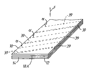
Items in Figure,? which are similar to items in Figures 1 to 6
are similarly referenced.
In the embodiment of Figure 7, the individual spacers 16 of
Figures 1 to 3 and the spacer 32 of Figures 4 to 6 are replaced
by a series of insulating spacers 39 extending widthwise of the
sensor at intervals therealong, each spacer being at an angle
CA 02296365 2000-O1-06
WO 99/09570 PCT/GB98/02424
9
to the length of the sensor. In this embodiment, the members
18,20 are replaced by a single continuous flexible conductive
layer or film 18A extending over substantially the whole of the
area lw. In the same manner as previously described, the spacers
39, in combination with the resilience of the cover layer 10,
ensure that there is no normal contact between the members 18A
and the conductive layer 14. In response to an applied force F,
however, and as explained in connection with the previous
embodiments, the cover layer l0 flexes and the conductive layer
18A over one or more of the gaps between the spacers 39 is
pressed into contact with the conductive layer 14 so as to
produce a detectable electrical signal.
The spacers 39 can be of any suitable cross-section so as to
provide electrically insulating separation between the member 18A
and the layer 14. The spacers 39 can be formed on the layer 14
by a normal printed-circuit technique. Instead, however, they
could be formed separately.
Advantageously, the angle ~ can be varied to alter the
sensitivity of the sensor without increasing the overall width
of the sensor. Additionally, the width of the spacers 80 can be
varied with the same result. Thus, increasing the angle
and/or increasing the width of the spacers 39 will decrease the
CA 02296365 2000-O1-06
WO 99/09570 PCT/GB98/02424
sensitivity of the sensor to the applied force F.
The sensors described above can be designed not only to respond
to a force applied to the uppermost surface shown in the Figures
but also to a force applied to the undersurface. This can be
achieved by making the layers 12 and 14 resiliently flexible.
The sensors shown in Figures 1 to 7 can be used in many
applications where it is required to produce an electrical signal
in response to an applied force. One particular application will
now be described, by way of example only, and relates to the
detection of an obstruction in a window opening in a motor
vehicle body which is closable by a motorised window glass. In
such cases, it is desirable to be able to detect the presence of
such an obstruction (e. g, part of the human body) so as to cause
immediate stopping of the window glass and avoiding consequent
injury.
As shown in Figure 8, a motor vehicle has a door 40 supporting
a window frame 42 in which a window glass 44 is upwardly and
downwardly slidable. The window glass 44 is raised and lowered
by means of an electric motor operable under control of an
occupant of the vehicle.
Figure 9 shows a section through the window frame 42, comprising
CA 02296365 2000-O1-06
WO 99/09570 PCT/GB98/02424
11
a rigid mounting channel 46 supported by inner and outer frame
members 48 and 49. The mounting channel 46 supports a window
sealing and guiding channel 50. The window channel 50 may be
made of extruded or moulded flexible material such as rubber or
plastics material. The distal edges of the side walls of the
channel have outwardly directed lips 52 and 54 which extend over
the corresponding edges of the mounting channel 46. Near the
base of the channel 50, it has further outwardly directed lips
56 and 58 which engage the cuxved-over edge regions of the frame
members 48 and 49 and resiliently hold the channel 50 within the
mounting channel 46.
The channel 50 also has lips 60 and 62 which extend across the
mouth of the channel and a further inner lip 64 near the base of
the channel. Figure 9 shows the window glass 44 which, as it
rises to the closed position, enters the channel 50 with the
outer surfaces of the lips 60 and 62 bearing against its opposite
faces and the lip 64 bearing against the edge of the glass. The
surfaces of the lips 60,62,64 which make contact with the glass
44 may be covered with a layer of flock 66 or other similar
material.
Within the distal edge of each side wall of the channel 50, a
force-responsive sensor 70 is embedded so as to run
longitudinally along the length of at least part of the channel
CA 02296365 2000-O1-06
WO 99109570 PCT/GB98/02424
12
50; advantageously, the sensors run along that part of the
channel 50 which extends along the top of the window opening and
down the "A" pillar of the vehicle to the region of the rear view
mirror. Advantageously, each sensor 70 has the form shown in
Figures 1,2 and 3, in Figures 4,5 and 6, or in Figure 7.
If an obstruction, such as part of the human body, is placed in
the window opening when the window glass 44 is wholly or
partially open, it will be carried upwardly by the closing window
glass and will cause a force F (see Figure 9) to be applied to
the distal edges of either or both of the side wails of the
channel 50, this force then being transmitted by the material of
the channel to the corresponding sensor. As explained in
conjunction with the earlier Figures, therefore, one or more of
the fingers 24 and/or 28 of the conductive members 18,20 (or the
conductive layer 18A in the case of the embodiment of Figure 7
will be moved into electrical contact with the conductive layer
14, thus producing an electrically detectable control signal.
This control signal can be used to cause immediate de-
energisation of the motor which is raising the window glass,
advantageously followed by reversal of the motor to lower it.
Each sensor 70 is preferably mounted in the channel 50 so that
the face shown uppermost in Figures 1,2 and 3, in Figures 4,5 and
6 or in Figure 7 faces downwardly in Figure 9. However, this is
not essential because the sensors can be arranged to respond to
*rB
CA 02296365 2000-O1-06
WO 99/09570 PCT/GB98/02424
13
a force applied to either of its major faces.
As shown in Figure 9, the base of the channel 50 is provided with
two longitudinally extending hollow chambers 72 to increase the
resilience of the side walls of the channel. The additional
resilience ensures that only a low reactive force is applied to
the obstruction by the window glass during the very short period
of time in which it may continue to rise after the sensor 70 has
produced the control signal. Clearly, the resilience of the side
wall must not be so great as to reduce the sensitivity of the
sensors. Figure 10 shows a modification in which the chambers
72 are omitted.