Note: Descriptions are shown in the official language in which they were submitted.
CA 02296403 2000-O1-14
WO 99/04493 PCT/EP9$/04352
-1-
ELECTRONIC ANALOGUE SWITCH
TECHNICAL FIELD OF THE INVENTION
The present invention relates to an electronic
analogue switch, and in particular to an analogue
switch using MOS transistors.
DESCRIPTION OF THE RELATED ART
Analogue switches including metal oxide semi-
conductor (MOS) transistors have conventionally
incorporated both p-channel and n-channel MOS
transistors. The n-channel transistor normally has its
body connected to the most negative power supply line
of the device. However, when the source of the NMOS
device goes more negative than the negative supply, a
PN junction diode between the source and the body of
the NMOS device will be forward biased. Thus current
will flow from the negative supply into the node to
which the analogue switch connects. This current flow
compromises the desired high OFF resistance of the
switch.
For example, a typical CMOS transistor switch is
shown and described in Figure 3.36 and on pages 142 and
143 of "The Art of Electronics", Horowitz and Hill, 2nd
Ed.. Cambridge University Press. A PMOS transistor is
connected in parallel with an NMOS transistor, the
transistors receiving logically opposite control
signals. This arrangement serves to ensure that the ON
resistance of the switch is desirably low. However, as
mentioned above, the OFF resistance is compromised when
the input drops below Ov, since this drop results in
fc>rward biasing the p-n junction in the NMOS
transistor.
SLf~~IMPRY OF THE PRESENT INVErITION
The present invention seeks to improve the maximum
allowable operating voltage of an analogue switch, when
the switch is ir_ the OFF position.
According to the present invention, there is
CA 02296403 2000-O1-14
WO 99/04493 PCT/EP98/04352
-2-
provided an analogue switch formed on a semiconductor
substrate, and comprising: input and output ports, a
first enhancement mode MOS transistor formed in an
ohmic isolated well in the substrate material and
having its gate connected to receive a control signal,
and having one end of its conducting channel and its
well connected to the input port, a second enhancement
mode MOS transistor formed in an isolated well in the
substrate, and having one end of its conducting channel
and its well connected to the input port, and having
its gate connected to the other end of the conducting
channel of the first transistor, a third enhancement
mode MOS transistor formed in an isolated well in the
substrate, and having its gate connected to receive the
complement of the said control signal, and having its
conducting channel connected between the output port
and the other end of the conducting channel of the
second transistor, and having its well connected to one
of the supply Lines of the switch, and control means
connected to the gate of the second transistor for
maintaining the second transistor in an opposite state
to that of the first transistor.
In one embodiment, each MOS transistor has its
conducting channel of the same type of semiconductor
material as the substrate, and is formed in a well of
semiconductor material of opposite type to that of the
substrate.
The substrate material may be n-type semiconductor
material, the wells being of p-type semiconductor
material and the transistors NMOS transistors. The
well of the third transistor is then connected to the
most negative supply line of the sw'_tcr. This
arrangement improves the malimum negative operating
voltaga when the switch is in the OFF position.
alternatively, the substrate material may be p-
type semiconductor material, the wells being of n-type
T.__~._....:-,......~.
CA 02296403 2000-O1-14
WO 99/04493 PCT/EP98/04352
-3-
semiconductor material, and the transistors PMOS
transistors. The well of the third transistor is then
connected to the most positive supply line of the
device. This arrangement improves the maximum positive
operating voltage, when the switch is in the OFF
position.
In an alternative embodiment, each transistor is
formed in a trench of an electrically isolating oxide
material. Each such MOS transistor may be an NMOS
device, with the well of the third MOS transistor
connected to the most negative supply line of the
switch, or each MOS transistor may be a PMOS device,
with the well of the third MOS transistor connected to
the most positive supply line of the switch
The control means preferably comprises a device
which tends to turn the second MOS transistor ON. Such
a control means may comprise an enhancement mode MOS
transistor having its gate connected to receive the
control signal and its conducting channel connected
between a power supply line and the gate of the second
transistor.
When the circuit transistors are NMOS, the
enhancement mode transistor is a PMOS transistor,
having its conducting channel connected to a positive
power supply line of the device.
Alternatively, the control means may comprise a
switched resistor.
BRIEF DESCRIPTION OF THE DRAWINGS
Figure 1 shows a circuit diagram of a conventional
analogue switch;
Figure 2 shows a general circuit diagram of a
first embodiment of the present invention;
Figure 3 shows a modification to the embodiment of
Figure 2;
Figure 4 shows a circuit diagram of a modification
to the embodiment o~ Figure 3; and
CA 02296403 2000-O1-14
WO 99/04493 PCT/EP98/04352
-4-
Figure 5 schematically illustrates the fabrication
of a MOS transistor used in the embodiments of present
invention.
DETAILED DESCRIPTION OF THE DRAWINGS
A conventional analogue MOS transistor switch 100
is shown in Figure 1, and comprises an NMOS transistor
101 and a PMOS transistor 102. The switch has an input
port 104 and an output port 105. The signal to be
switched is connected to the input port 104, and is
transmitted to the output port 105 when the switch is
in an ON state. The gate G of the NMOS transistor 101
is connected to a control signal input 107, and the
gate G of the PMOS transistor 102 is connected to a
control signal input 108.
The body of the NMOS transistor is connected to
the most negative supply line of the device, whilst the
body of the PMOS transistor is connected to the most
positive supply line. In the case shown in Figure 1,
these supply lines are at Ov and 5v respectively.
When the control input 107 is low (i.e. Ov) and
the control input 108 is high (i.e. 5v) the switch is
in an OFF condition, and so no current is transmitted
between the input and output ports 104 and 105.
However, if the signal at the input port 104
should drop below the voltage to which the body of the
NMOS transistor is connected (Ov) then the PN junction
diode formed between the body and source of the NMOS
transistor 101, becomes forward biased. Thus, current
can flow from the negative supply into the input node.
Any such current flow compromises the desired high OFF
resistance of the switch.
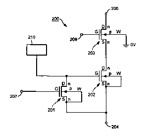
Figure 2 shows a first embodiment 200 of the
present invention, which comprises first, second and
third NMOS trar_sistors 201, 202 and 203. The first
NMOS transistor 201 is connected to a control input 207
at its gate G. The source S and well ~,~1 of the first
_.___....__..__ __
CA 02296403 2000-O1-14
WO 99/04493 PCT/EP98/04352
_5_
MOS transistor 201 are connected to an input port 204
of the device. The transistor 201 thus operates in
enhancement mode.
The second and third MOS transistors 202 and 203
are connected with their conducting channels in series
between the input port 204 and an output port 205 of
the device. That is, the source S of the transistor
202 is connected to the input port, the drain D of the
transistor 202 is connected to the source S of the
transistor 203, and the drain D of the transistor 203
is connected to the output port 205. The gate G of the
second MOS transistor 202 is connected to the drain D
of the first MOS transistor 201 and to a control device
210.
The gate G of the third transistor 203 is
connected to a second control input 208, which receives
the complement of the signal applied to the first
control input 207, and the well W of this device is
connected to the most negative supply line of the
switch.
The control device 210 is connected to the gate G
of the second transistor 202 and operates to try to
switch that transistor 202 to an ON state, in
opposition to the first MOS transistor 201.
For the switch to be in an OFF condition, a high
(5v) control signal is applied to the control input
207, and a low (Ov) control signal applied to the
control input 208. The high control signal turns
transistor 201 ON, which causes the gate G of the
transistor 202 to be pulled down to the voltage level
of the input port 204. Thus the gate-source voltage
Vgs of the transistor 202 is held at Ov, which ensures
that the transistor 202 remains in an OFF condition.
The gate G of the third transistor 203 is held at
Ov in this OFF cor_dition, which e:~suras that the third
transistor 203 also remains in an GF- con3itior_.
CA 02296403 2000-O1-14
WO 99/04493 PCT/EP98/04352
-6-
The control device 210 operates to ensure that the
second MOS transistor turns ON successfully when the
switch is ON. The device could be provided by a PMOS
transistor, a switched resistor, an unswitched resistor
or a current source, provided by MOS or bipolar
devices.
In order to turn the switch ON, a low (Ov) signal
is applied to the control input 207, and a high (5v)
signal to the control input 208. These signals turn
the first transistor 201 OFF, which allows the device
210 to pull the second transistor ON. The third
transistor is also pulled ON, and so the switch is in
an ON state.
Unlike in the previously-considered circuit of
Figure l, the PN junctions of the transistors 201 and
202 between the source and body of those transistors,
remain unbiased in the OFF state, even if the voltage
at the control input 204 becomes more negative than the
negative supply voltage by a voltage up to the
threshold voltage of the transistor 201. As a result,
leakage current cannot flow between the input and
output ports 204 and 205 of the switch.
Thus the OFF state negative voltage range which
can be applied to the input port 204 is much improved
over the previously-considered circuit design. The
maximum negative voltage possible is then primarily
based on the reverse bias breakdown voltages of the
reversed biased PN junctions between the well W and
drain D of the respective transistors, and is limited
by the threshold value of transistor 201.
It will be appreciated that although Figure 2
shows only NMOS devices, the transistors of the circuit
embodying the present invention could be PMOS devices.
Figure 3 shows a modification of the Figure 2
circuit, in which the device 210 is constituted by a
PMOS transistor 211. An inverter 212 is connected
T ..__~..__~_..___._.._._ _
CA 02296403 2000-O1-14
WO 99/04493 PCT/EP98/04352
_7_
between the control input 207 and the gate of the third
transistor 203 in order to provide that transistor with
the complement of the control signal supplied to the
input 207.
In addition, a second PMOS transistor 213 is
connected in parallel with the second and third NMOS
transistors 202 and 203, and is connected to receive a
control signal 214. As in the conventional circuit
shown in Figure 1, the PMOS transistor 213 serves to
reduce the ON resistance of the switch, and is turned
ON by a low input control signal.
The Figure 3 circuit has all the advantages of the
Figure 2 circuit, and in particular the maximum
negative voltage allowable at the input port 204 when
the switch is in an OFF position is improved over prior
art devices.
The PMOS transistor 211 receives the control
signal from the control input 207, so that when the
first NMOS transistor 201 is ON, the PMOS transistor
21.1 is OFF, and vice versa. This PMOS transistor 211
acts to ensure that the second NMOS transistor 202 is
pulled into an ON state when the switch is turned ON.
If the PMOS transistor 211 or other device was not
provided then, when the transistor 201 is OFF, the gate
voltage of the second NMOS transistor 202 will float,
which leads to uncertainty of the overall switch
condition.
Figure 4 shows an improvement of the Figure 3
design, in which an additional diode 215 is included
between the source S and well W connection of the first
NMOS transistor 201 and the input port 204.
The diode 215 serves to increase the magnitude of
the negative voltage which can be applied to the port
204 when the switch is ON by the diode forward voltage
drop value. Specifically, when the switch is ON, an
unwant°~' current which would otherwise flow from the
CA 02296403 2000-O1-14
WO 99/04493 PCT/EP98/04352
_g_
input port 204 through the channel of device 201 is
blocked until the negative voltage applied to port 204
equals a voltage equal to the sum of the threshold
voltage of the transistor 201 and the forward voltage
drop of the diode 215.
In such a design, the gate-source threshold
voltage Vt of the second MOS transistor 202 must be
greater than the forward voltage drop of the diode so
that, when transistor 201 is ON, it can hold transistor
202 in an OFF condition.
It will be appreciated that embodiments of the
present invention have been described with specific
reference to specific types of MOS transistors, and
that the opposite type of MOS transistor is readily
used in place of those described.
For example, the third MOS transistor could be a
PMOS transistor, in which case its well would be
connected to the most positive supply line of the
device.
It will also be readily appreciated that each
transistor in the circuits described can be replaced by
a plurality of parallel or serial devices.
Alternatively, the second and/or third transistors
could be replaced by a plurality of devices whose
channels are connected in series with one another and
whose gates are common. The well connections for such
series devices would be common to one another.
The first MOS transistor could be replaced by a
plurality of devices whose channels are connected in
series and whose gates are common. The wells could
either be common and connected to the input port or
separate with each well connected to the end of the
channel which is nearest to the input port.
The embodiment of the ir_vention described in
Figures 2, 3 and 4, can advantageously exploit the
characteristics of trench isolatior_.
_. ___._._.._.. _. r
CA 02296403 2000-O1-14
WO 99/04493 PCT/EP98/04352
-g_
In such trench isolation the MOS devices are
placed in separate ohmic isolated trenches. Figure 5
shows a schematic diagram of one such MOS device.
The device is formed on a substrate 50 and has its
well 52 isolated from the substrate material by an
oxide layer 51. The substrate material is of p-type or
n-type, and the well material can also be of either
type of material (n-type for PMOS transistors, p-type
for NMOS transistors). A conducting channel 53 is
created between the drain and source connections 54 and
55 of the device. The conduction is controlled by a
gate terminal 56 in conventional manner.
Alternatively, the MOS transistors can be
"junction isolated" from the substrate material by
forming the wells of opposite type semiconductor
material from the substrate semiconductor material.