Note: Descriptions are shown in the official language in which they were submitted.
CA 02296722 2000-O1-06
WO 99/05745 PCT/US98/18243
BATTERY TESTER HAVING PRINTED ELECTRONIC COMPONENTS
The present invention generally relates to circuits for displaying information
relating
to batteries, particularly for battery tester circuits, and to battery labels
that incorporate
such circuits.
Battery tester circuits exist that may be printed on a battery label. Such
battery tester
circuits are typically either "thermochromic" testers or "electrochromic"
testers.
Thermochromic testers include a calibrated resistor that may be selectively
coupled to the
opposite poles of the battery through a switch that is provided at either or
both ends of the
calibrated resistor. A layer of thermochromic ink is printed over the resistor
and responds to
changes in the temperature of the calibrated resistor by gradually changing
between transparent
and opaque states, thereby enabling indicia printed under the thermochromic
layer to be viewed
or blocked, depending on the temperature of the calibrated resistor.
Alternatively, the
thermochromic layer may change colour in response to changes in the
temperature of the
calibrated resistor.
The temperature of the calibrated resistor is determined by the power which
the battery
can deliver, which is a function of both the voltage and the internal
resistance of the battery.
The accuracy of a thetmochromic tester is determined not only by the rate of
change of the open
circuit voltage and internal resistance, representing the rate of change of
the battery's ability to
produce power, but also by the responsivity of the thermochromic ink to
temperature changes,
i.e. the size of the temperature change required to cause the thermochromic
ink to change
colour. Thus, the thermochromic ink layer functions both as a display and as a
sensor, and the
accuracy of the tester can be limited by the temperature responsivity of the
thermochromic ink.
CA 02296722 2000-O1-06
WO 99/05745 PCT/US98/18243
2
Electrochromic testers differ from thermochromic testers in that the display
layer
changes colour directly in response to changes in the open circuit voltage of
the battery. The
accuracy of an electrochromic tester is determined by the rate of change of
the open circuit
voltage of the battery with depth of discharge, and by the responsivity of the
electrochromic
material to voltage changes. Thus, like the thermochromic tester, the
electrochromic tester
display functions both as a display and as a sensor, and the accuracy of the
tester may be limited
by the responsivity of the electrochromic material.
Since the accuracy of these thermochromic and electrochromic testers is
limited by the
response of the display, it has been proposed to improve tester accuracy by
including a voltage-
responsive electronic component, such as a Zener diode or transistor, and thus
to limit the
function of the display to displaying information. Such an approach is
disclosed in US-A-
5,610,511, US-A-5,460,902, and US-A-5,389,470. In these patents, tester
circuits are
disclosed that utilise discrete electronic components to discriminate between
various discharge
levels and to selectively activate different segments of a thernnochromic
display. Thus, these
tester circuits provide discrete displays for the various discharge levels
that are discriminated by
a separate sensing circuit, thereby limiting the function of the display to
that of an actual display.
However; because the testers disclosed in these patents utilise discrete
electronic
components manufactured using conventional semiconductor technology, the
electronic
components are not sufficiently small to be included in the label of a
battery. Further, because
the exterior dimensions of batteries are strictly limited by various national
and international
standards, such electronic components cannot be provided on the exterior
surface of a battery.
If such electronic components were to be provided in the interior of a,
battery, the space
occupied by the electronic components would reduce the space available for
active battery
ingredients, thereby reducing the service life of the battery. For these
reasons, the use of a
CA 02296722 2000-O1-06
W0 99/05745 PCT/US98/18243
3
separate voltage discrimination circuit for an on-label tester has not been
commercially
implemented.
Another problem associated with thermochromic and electrochromic testers
concerns the
amount of power consumed by these testers. Because these testers consume
relatively significant
levels of power, switches are provided to enable selective activation of the
testers and thus to
avoid a constant drain on the battery. Because of the requirement for such
switches, however,
the displays do not continuously display the discharge level of the battery.
Although general purpose electric field-responsive liquid crystal displays are
known,
they are too expensive to be included in a battery label and require
activation voltage levels well
in excess of the open circuit voltage of most batteries. Further, these liquid
crystal displays tend
to polarise irreversibly when driven by a direct current (DC) driving signal.
For these reasons,
electric field-responsive liquid crystal displays have been considered to be
unsuitable for use in
on-label battery testers.
It would therefore be desirable to provide a tester circuit for displaying
information
relating to the status of a battery, which is not constrained by the accuracy
limitations
associated with thermochromic and electrochromic displays and which may be
provided on
the exterior surface of a battery or form part of a battery label. It would
also be desirable
to provide a more accurate battery tester circuit on a battery label.
Accordingly, in a first aspect, the present invention provides a battery
tester circuit
comprising a display component for displaying information relating to the
status of a battery
and a display driver component for receiving power from the battery to drive
the display
component, wherein at least one of the components is printed on a substrate.
In a preferred embodiment of this first aspect of the present invention, the
display
component comprises a display printed on the substrate for displaying an
indication of the
CA 02296722 2000-O1-06
W0 99105745 PCT/US98I18243
4
level of discharge of a battery, and the display driver component comprises a
display driver
circuit coupled to the display and to the battery for receiving power from the
battery to
drive the display and a battery discharge level sensing circuit coupled to the
display and to
the battery for sensing a discharge level of the battery and for supplying a
display signal
representing the sensed discharge level to the display, wherein at least one
of the circuits is
printed on the substrate.
In a second aspect, the present invention provides a battery label comprising
a label
substrate for covering an outer portion of a battery, and an electric field-
responsive liquid
crystal display printed on an outer surface of the label substrate for
displaying information
relating to the status of the battery.
In a third aspect, the present invention provides a battery comprising an
electrochemical cell provided in a battery housing and having a positive
terminal and a
negative terminal, and a battery tester circuit as described above, wherein a
label substrate
is disposed on an exterior surface of the battery housing, a discharge level
sensing circuit is
directly coupled to the terminals for continuously sensing a discharge level
of the battery,
and the display component is a liquid crystal display printed on the label
substrate and
coupled to the discharge level sensing circuit for continuously displaying an
indication of
the sensed level of discharge of the battery.
By providing a display driver component to drive the display component, the
function of the display component has been specifically restricted to that of
displaying
information, thus avoiding accuracy limitations associated with known display
arrangements
in which the display material also acts as a sensor. Moreover, by using a
component that is
printed, the tester circuit can be made sufficiently compact for applications
where space is
at a premium, such as in on-label battery tester circuits.
*rB
CA 02296722 2000-O1-06
WO 99/05745 PCTII1S98/18243
The substrate may be any suitable material that can be used in connection with
batteries, and is conveniently selected from a battery label, a battery pack
housing, a
flashlight housing, battery packaging material, or a housing of any other
device in or with
which batteries are used. The substrate material is appropriately chosen from
any materials
that can support or contain printed components, such as plastics or paper
materials. In a
preferred embodiment, the substrate is a battery label. In this case, the
label substrate may
for example be a laminated or single-layer structure, and preferably is formed
of at least one
layer of PVC material.
The display component may be any type of display that can be activated by a
suitable display driver so as to selectively present or conceal visible
information to a
viewer. Preferably, the display component comprises a liquid crystal material
that is
electrically activatable. More preferably, the display component is an
electric field-
responsive liquid crystal display.
Although the display component is described herein as being provided primarily
for use
in connection with a battery tester, it will be appreciated that the display
may be provided on a
battery label to display other information pertaining to the battery. Such
information may
include advertisements and/or other information or graphics for attracting a
consumer's
attention. Since, advantageously, the disclosed display may be continuously
left in an ON state,
the displayed information may periodically alternate between, for example, a
graphics
advertisement and the battery discharge level. Further, a switch may be
provided in the battery
label to initiate manually a change in the information displayed.
As mentioned above, the display component in the display circuit in accordance
with the
invention is used solely for the purpose of displaying information to the
consumer. To this end,
a separate display driver component is used to drive the display component,
thereby limiting the
CA 02296722 2000-O1-06
W0 99/05745 PCT/US98I18243
6
function of the display component to that of a display only. The display
driver component
may be any suitable circuit or device that can be powered by the battery and
can activate the
display in any manner that does not require the display to function as a
sensor for the
information to be displayed.
The display driver component preferably provides a discriminating function to
classify
information relating to the status or condition of the battery into
appropriate classifications.
Preferably, the display driver component provides a voltage discrimination
function. For
example, a voltage discriminating circuit may be included as part of or as the
display driver
component in order to compare the sensed open circuit voltage of the battery
to generated
reference values to determine whether the remaining cell capacity of the
battery is fresh, good,
or fully discharged. For example, for a AA alkaline Zn-Mn02 cell, the open
circuit voltage
may fall from around 1.55 volts to 1.05 volts. Thus, the voltage
discriminating circuit is
preferably configured to activate one or all the display segments for cell
voltages at or above
1.50 volts, to activate two or all but one display segments at voltages
between for example 1.40
and 1.49 volts, and so on, to provide an indication representing a gradual
change in cell
discharge level.
Details arid operation of a suitable voltage discriminating circuit as shown
in Figure 5 are
described in US Patent No. 4,027,231. Other suitable voltage discriminating
circuits are
disclosed in US Patent Nos. 5,460,902 and 5,610,511.
The voltage discriminating circuit is preferably formed by printing the
various elements
and connectors directly onto a libel substrate or on a protective layer for
the display.
Techniques for printing resistors in this manner are known and used in
printing thermochromic
battery testers. Techniques for printing transistors and diodes using polymers
are also generally
known and described in an article by Francis Gamier et al., entitled "All-
Polymer Field-Effect
*rB
CA 02296722 2000-O1-06
WO 99/05745 PCT/US98/18243
7
Transistor Realized by Printing Techniques" appearing in Science, Vol. 265,
September 16,
1994; and in an article by A.R. Brown et al. entitled "Logic Gates Made From
Polymer
Transistors and Their Uses in Ring Oscillators", Science, Vol. 270, November
10, 1995.
An example of a metal-insulator-semiconductor FET (MISFET) transistor printed
using
such polymers is shown in cross-section in Figure 6. The MISFET as shown
includes an
insulating layer that may be formed, for example, of a 1.5 pm thick polyester
film polyethylene
terephthalate. A gate electrode may be printed on one of the faces of the
insulating film, for
example as a 10 ~m thick layer of a conducting graphite-based polymer ink. The
MISFET also
includes a device substrate that may be made, for example, of a 10 x 15 mm
sized adhesive tape
with electrical contact for the gate electrode made from the same conducting
polymer ink. The
source and drain layers of the MISFET may be formed, for example, using two 1
x 10 mm
strips that are 10 ~m layer thick, of the same conducting graphite-based
polymer ink.
Preferably, the source and drain electrodes are deposited through a mask with
a 200 ~,m
interelectrode distance. The MISFET further includes an organic semiconducting
layer that may
be formed, for example, of a, cu-di(hexyl)sexithiophene, deposited between the
source and drain
layers.
It will be appreciated that other discriminating circuits may be used in the
display driver
component, instead of or additional to a voltage discriminating circuit, in
order to classify other
sensed properties relating to the performance status or condition of the
battery into
classifications. Furthermore, it will be appreciated that if additional
display segments are
provided in order to display additional indications, the discriminating
circuit will preferably
classify the sensed information into additional classifications to correspond
to the number of
display segments.
CA 02296722 2000-O1-06
WO 99/05745 PCT/US98/18243
8
If an electric field-responsive liquid crystal display is used as the display
component,
then the display driver component preferably provides an oscillator function
in order to
drive the display with an alternating current and thus to preclude
irreversible polarisation of
the display. In this case, the display driver component preferably provides
both an
oscillator function and a voltage discrimination function.
Because in certain circumstances the voltage required to drive the display
component
may exceed that of the open circuit voltage of the battery and, as mentioned,
because electric
field-responsive liquid crystal displays are preferably driven using an
alternating current {AC)
signal rather than a direct current (DC) signal, a voltage multiplying and/or
oscillating circuit
may be included in the display driver component for driving the display. The
frequency of the
AC driving signal generated by the circuit may be selected appropriately, and
is preferably less
than 10 kHz. The voltage levels of the circuit may also be chosen
appropriately, and preferably
are in the range of 3 to 50 volts. A suitable oscillating circuit that may be
formed using polymer
transistors suitable for printing on a substrate is shown in Figure 7, as
described by A.R. Brown
et al. in an article entitled "Logic Gates Made From Polymer Transistors and
Their Uses in Ring
Oscillators", Science, Vol. 270, November 10, 1995. As shown, the ring
oscillator includes
five inverter gates formed of a plurality of MISFETs. The oscillator circuit
shown may have an
oscillating frequency in the range of 10-500 Hz. The MISFETs may be printed
and configured
in the same manner as shown in Figure 6. Examples of capacitive voltage
doubter circuits
capable of producing an AC signal at double the input voltage are described in
Maxim 1989
Integrated Circuits Data Book, pp. 6-119; and in F. Mazda, Electronic
Engineer's Reference
Book, 5th Ed., Butterworths, 1983, Chapters 39 and 42.
The positioning of the various circuits in the display driver component may be
selected
as appropriate. Thus, the voltage multiplying/oscillating circuit is
preferably arranged between
CA 02296722 2000-O1-06
WO 99/05745 PCT/US98/18243
9
the battery terminals and a voltage discriminating circuit, as for example
shown in Figure 3.
Alternatively, the positioning of these circuits in the display driver
component may be reversed
such that the voltage discriminating circuit selectively enables the voltage
multiplying/oscillating
circuit to deliver an AC driving signal to a selected display segment.
However, by arranging a
voltage multiplying circuit in the manner shown in Figure 3, the voltage
discriminating circuit
will be presented with a greater range of voltages, thereby increasing its
ability to discriminate
between various voltage levels.
Since in accordance with the present invention at least one of the display
component
and display driver component is printed on a substrate, the advantages in
terms of space
saving can be realised even when only one of the components is printed.
However,
preferably both components are printed on the substrate, in order to maximise
the space
saving advantages.
It will be appreciated that the display driver component may comprise a
plurality of
circuits or functional modules, for example for implementing voltage
discriminating and
voltage multiplying/oscillating functions, as mentioned above. One or more of
these circuits
may be printed on the substrate. Preferably, however, all of the constituent
circuits of the
display driver component are printed. The circuits are preferably formed by
printing
processable conductive polymer material layers on the substrate. In this
manner, a battery tester
circuit in accordance with the present invention may conveniently be printed
on a battery label
using conventional printing techniques.
As mentioned, the display component preferably is an electric field-responsive
liquid
crystal display and, as such, includes at least one layer of liquid crystal
material that undergoes a
change in visual appearance in response to an electric field applied across
the layer of liquid
CA 02296722 2000-O1-06
WO 99105745 PCTlUS98118243
l0
crystal material. The electric field-responsive liquid crystal display may be,
for example,
birefringent or bipolar.
The display may include a graphics layer to provide indications such as
"fresh", "good"
and "replace", or any other appropriate indications descriptive or informative
of the status or
condition of the battery according to the selected battery property being
tested. Although any
appropriate method may be used to provide the indications, the indications are
conveniently
printed using conventional printing techniques. Conventional inks can be thus
be used to
provide high contrast indications visible to the viewer when the display is
activated or
deactivated.
It will be appreciated that one or a plurality of indications may be provided
to present
information relating to the status or condition of the battery. If more than
one indication is to be
made visible or invisible, the display preferably comprises a corresponding
number of
individually activatable segments. Thus, indications printed in a graphics
layer, or otherwise
provided, may be selectively concealed or revealed by the selected activation
of a corresponding
segment the display.
It will be appreciated that with an electric-field responsive liquid crystal
display in which
indications are provided in a graphics layer, the indications may be concealed
either by being
blocked by the liquid crystal layer or by disappearing against a non-
contrasting background
provided or revealed by the liquid crystal layer, according to whether the
graphics layer is
positioned behind or in front of the liquid crystal layer, when viewed.
It will further be appreciated that the position of graphics layer may be
varied behind the
liquid material, for example so as to be disposed between the outer surface of
the substrate and
an electrode, or between an electrode and the liquid crystal material, or on
the inner surface of
CA 02296722 2000-O1-06
WO 99/05745 PCT/US98/18243
11
the substrate, provided that the indications are made visible to the viewer
when they are not
selectively blocked by liquid crystal material.
Alternatively, the graphics layer may be disposed in front of the liquid
crystal material,
for example between an electrode and a protective covering layer or between an
electrode and
the liquid crystal material, so that the liquid crystal material selectively
determines the
background against which the indications appear. In this case, a liquid
crystal layer may for
example constitute or expose behind it a non-contrasting background for the
indications, so that
the indications are concealed until the liquid crystal layer is selectively
activated, or alternatively
deactivated, whereupon it provides or exposes a contrasting background in
order to show up and
thus reveal the indications. Thus, the graphics layer may be disposed in front
of the liquid
crystal layer in any suitable position provided that the indications can
selectively be concealed
against or brought out in contrast against a background when the liquid
crystal layer is activated.
It will further be appreciated that the liquid crystal display may be applied
either to the
outer surface or to the inner surface of a label substrate. If applied to the
inner surface, the
liquid crystal display will be viewed through the label substrate.
Accordingly, the substrate will
preferably be transparent or be provided with a transparent window to allow
the indications to be
viewed.
Each display segment generally comprises paired electrodes that can generate
an electric
field between them on application of a potential difference. A separate set of
electrodes can be
provided for each display segment. Alternatively, one member of each electrode
pair may be
shared between segments. Such segments may be completely isolated from one
another or share
a common liquid crystal layer.
In an electric field-responsive liquid crystal display, the electrodes may
suitably be
formed of any conductive material, for example of a transparent conductive
material such as tin-
CA 02296722 2000-O1-06
WO 99/05745 PCT/(TS98/I8243
12
doped indium oxide (ITO), of a thin transparent metal coating formed by vapour
deposition or
sputtering, or of printing inks that use transparent conductive particles such
as tin-doped indium
oxide, antimony-doped tin oxide, fluorine-doped tin oxide, or zinc oxide.
Other suitable
materials will be apparent to those skilled in the art. Preferably, the
electrodes are formed from
a much less-expensive solution processable conductive polymer such as
dodecylbenzene
sulphonic acid doped polyaniline, which may be dissolved in a suitable solvent
such as toluene.
This material is relatively inexpensive and is particularly well-suited for
printing as a layer on a
substrate or on an adjacent layer, as is desirable for the mass production of
tester displays.
It will be appreciated by those skilled in the art that in a liquid crystal
display intended to
be viewed from the top, as shown for example in Figure 2A, the bottom
electrode may be
reflective or opaque, instead of transparent. If the bottom electrode is
reflective or opaque, the
graphics layer is preferably formed on top of the bottom electrode so that it
will be visible
through the liquid crystal layer. It will further be appreciated that if a
liquid crystal display is
intended to be viewed from the bottom, for example through the substrate as
shown in Figure
2A, and a graphics layer is formed above the liquid crystal layer, then the
top electrode may be
reflective or opaque, and the graphics layer will then preferably be formed
below the top
electrode.
The liquid crystal layer may be formed from any suitable electric-field
responsive liquid
crystal materials known in the art, but is preferably formed of a polymer
liquid crystal (PLC) or
polymer-dispersed liquid crystal (PDLC) material that may be printed on an
adjacent layer using
conventional printing techniques. Suitable PLC materials are disclosed in US-A-
5,397,503.
In PDLC materials, the liquid crystal material is isolated either in
microcapsules
embedded in a solid polymer matrix or in micelles in a polymer matrix. The
polymer matrix is
preferably chosen so that the polymer and liquid crystal material have equal
refractive indices in
CA 02296722 2000-O1-06
WO 99/05745 PCTIUS98/18243
13
the presence of a particular electric field. Thus, in an electric field when
the respective indices
are the same, the material appears clear. When the electric field is removed
or altered, the
refractive indices become different, incident light is scattered and the
material appears cloudy or
black with suitable dye additives. Alternatively, the materials may be so
chosen as to appear
opaque in a certain electric field and transparent in the absence of an
electric field or in a
different electric field. Examples of birefringent PDLC displays are disclosed
in US-A-
5,202,063, US-A-5,285,299 and US-A-5,225,104.
The liquid crystal display preferably includes one or more protective layers
made of a
transparent material such as PVC. It will be appreciated that the graphics,
electrode, liquid
crystal and protective layers, as appropriate, may be printed in any
convenient order. For
example, layers 30, 34, 36, and 38 in Figure 2A may be printed first on label
substrate 32 and
then adhered to protective layer 40 or, alternatively, may be printed on
protective layer 40 in
reverse order and then adhered to label substrate 32. Other methods of forming
this and the
other structures disclosed herein will be apparent to those skilled in the
art.
In a preferred embodiment, a liquid crystal display is used that comprises a
plurality of
liquid crystal layers instead of a single layer. Advantageously, by using a
plurality of thinner
liquid crystal layers, the voltage required to activate and drive the liquid
crystal display may be
significantly reduced. A plurality of such thinner liquid crystal layers is
preferred because,
although individually the change in visual state of each thinner liquid
crystal layer will be less
perceptible, the changes in visual state of each layer will be cumulative,
thereby providing a
sufficient overall change in visual appearance of the display between its
activated and inactivated
states.
For a single layer display, as shown for example in Figure 2A, the liquid
crystal layer
has a thickness for example of 1.5 to 2.0 pm and is preferably powered by
applying a 4- to 5-
CA 02296722 2000-O1-06
WO X9/05745 PCT/US98118243
14
volt potential difference across the liquid crystal layer. In a mufti-layer
display, as shown for
example in Figure 2B, the liquid crystal layers may be sufficiently thin such
that a potential
difference of 1.5 volts need only be applied across each layer to cause a
sufficient overall change
in visual states. It will be appreciated that the display may include any
number of liquid crystal
layers, and that the thinness of each layer may be selected accordingly.
In the mufti-layer display, each liquid crystal layer can be activated by the
electrodes
adjacent to each layer. Thus, two adjacent liquid crystal layers can
conveniently share a
common, preferably transparent, electrode disposed between the layers. If each
liquid crystal
layer in the display is intended to be activated at the same time, alternating
electrodes are
preferably electrically coupled together such that only two electrical
connectors need to be
provided for delivering power to activate the display or display segment.
The battery tester circuit of the present invention may be permanently
electrically
connected or coupled to the positive and negative battery terminals so that
the tester is
permanently 'ON', or may be so constructed that either or both ends of the
circuit are normally
uncoupled from the respective battery terminals, in an 'OFF' mode, until
electrically connected
or coupled by the consumer, to an 'ON' state. In the latter case, one or more
switches may be
provided for operation by the consumer in order to selectively connect or
couple the battery
tester to the battery terminals. Suitable switching mechanisms are known in
the art. Preferably,
and particularly if a low power consuming electric field-responsive liquid
crystal display is used
as the display component, the tester circuit is permanently connected or
coupled to the battery
terminals so as to monitor the status or condition of the battery. Thus, with
such a direct and
permanent electrical connection, the battery testing circuit may continuously
monitor cell
capacity, for example, and provide a continuous display of the remaining
capacity.
CA 02296722 2000-O1-06
WO 99/05745 PCT/US98/18243
The present invention will now be further illustrated with reference to the
accompanying drawings, in which:
Figure 1 is a perspective view of a battery incorporating an on-label battery
tester circuit
constructed in accordance with an embodiment of the present invention;
Figure 2A is a partial cross-sectional view taken along plane II-II of Figure
1 illustrating
a liquid crystal display suitable for use in accordance with the present
invention;
Figure 2B is a partial cross-sectional view taken along plane II-II of Figure
1 illustrating
a further liquid crystal display suitable for use in accordance with the
present invention;
Figure 3 is an electrical circuit diagram in block form of a battery tester
circuit
constructed in accordance with a preferred embodiment of the second aspect of
the present
invention;
Figure 4 is a perspective view of a battery provided with a tester circuit as
represented in
Figure 3, in which the protective outer layer has been removed to show
exemplary positioning
of the elements on the base layer of a battery label, in accordance with an
embodiment of the
third aspect of the present invention;
Figure 5 is an electrical circuit diagram in block and schematic form showing
an
exemplary construction of a display driver circuit (voltage discriminating
circuit) coupled to a
liquid crystal display in accordance with an embodiment of the first aspect of
the present
invention;
Figure 6 is a cross-sectional view of an exemplary construction of a
transistor that may
be printed on a label using conductive and semiconductive inks, suitable for
use as a component
in a display driver circuit.
CA 02296722 2000-O1-06
WO 99!05745 PCT/US98/18243
16
Figure 7 is an electrical circuit diagram in schematic form illustrating an
exemplary
construction of a display driver circuit (oscillating circuit) suitable for
use in a display circuit in
accordance with the present invention;
Figure 8 is an electrical circuit diagram in block form illustrating a battery
tester circuit
comprising a liquid crystal display coupled to a display driver circuit, in
accordance with a
preferred embodiment of the present invention; and
Figure 9 is an electrical circuit diagram in block form illustrating a battery
tester circuit
comprising a liquid crystal display coupled to a display driver circuit, in
accordance with another
embodiment of the present invention.
As shown in Figure 1, a battery 10 has a label 15 incorporating a battery
testing circuit.
The battery testing circuit includes a mufti-segmented display 20 having
segments 22a-22c that
may be selectively activated so as to display the discharge level of the
battery 10. A first
segment 22a is arranged to indicate "fresh" when the remaining battery
capacity is relatively
high, a second segment 22b to indicate "good" when the battery discharge level
is sufficient for
most applications, and a third segment 22c to indicate "replace" when the
remaining battery
capacity is too low for use in most applications.
Figures 2A and 2B show preferred displays for use in accordance with the
present
invention. The displays 20 are electric field-responsive liquid crystal
displays that undergo a
change in visual appearance in response to an electric field applied across
the liquid crystal
material. As shown in Figure 2A, the liquid crystal display 20 includes a
graphics layer 30 that
is printed on the outer surface of a label substrate 32. The graphics layer 30
is positioned behind
a liquid crystal layer 36 and transparent electrodes 34 and 38, as viewed
through transparent
protective layer 40. Thus, graphics layer 30 may be selectively blocked or
exposed by selective
activation of liquid crystal layer 36 via electrical connectors 58 and 60. In
the display shown in
CA 02296722 2000-O1-06
WO 99!05745 PCTJUS98118243
17
Figure 2B, two liquid crystal layers are used in place of the single liquid
crystal layer 36
described above in Figure 2A. As shown in Figure 2B, a graphics layer 30 is
printed on a label
substrate 32. A first transparent electrode 42 is printed on graphics layer
30. On transparent
electrode 42 is printed a first liquid crystal layer 44. A second transparent
electrode 46 is
printed on an opposite side of liquid crystal layer 44. A second liquid
crystal layer 48 is printed
on second transparent electrode 46, and a third transparent electrode 50 is
printed on second
liquid crystal layer 48. A transparent protective layer 56 is provided over
the structure.
Electrodes 42 and 50 are electrically coupled to connector 60 and electrodes
46 and 54 are
electrically coupled to connector 58.
As illustrated in Figure 3, a voltage multiplying/oscillating circuit 72 is
coupled to the
positive and negative terminals of a battery by conductive strips 78 and 80.
Voltage
multiplying/oscillating circuit 72 delivers an AC driving signal over
connectors 74 and 76 to a
voltage discriminating circuit 70, which in turn drives the segments 22a, 22b
and 22c of liquid
crystal display 20 via connectors 58 and 60a, 60b and 60c.
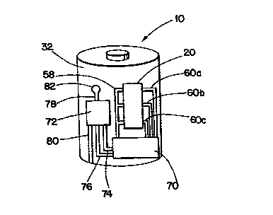
Figure 4 shows a battery 10 with protective layers removed to expose the
relative
positioning of the components of the battery tester circuit as illustrated in
Figure 3. As shown in
Figure 4, a conductive strip 80 extends along label substrate 32 to an edge
thereof in contact
with the negative terminal of battery 10. The negative terminal is
electrically insulated from the
battery can and positive terminal, and the can is electrically connected to
the positive terminal.
A conductive strip 78 may contact the battery can through a hole provided in
the label substrate
32 by means of a switch pad 82. Thus, the tester circuit may be selectively
coupled to the
positive terminal of the battery by a consumer, through depression of the
switch pad 82.
Figure 5 shows an exemplary circuit for implementing a voCtage discriminating
circuit
70. As shown in Figure 5, voltage discriminating circuit 70 includes a
resistor dividing network
*rB
CA 02296722 2000-O1-06
WO 99/05745 PCT/fJS98118243
18
including a first resistor 90 having a first end connected to connector 74 and
a first end of a
second resistor 92. Connector 74 may be coupled to the positive output
terminal of voltage
multiplying/oscillating circuit 72 as shown in Figure 3. The second end of
first resistor 90 is
coupled to connector 58 which is coupled to one or more of the transparent
electrodes that are
part of liquid crystal display 20. Second resistor 92 has its second end
connected to a first end
of a third resistor 94 and to a first end of a fourth resistor 96. Third
resistor 94 has its second
end coupled to the gate of a first transistor 98. Fourth resistor 96 has its
second end connected
to a first end of a fifth resistor 100 and to the first end of a sixth
resistor 102. Fifth resistor 100
preferably has its second end connected to the gate of a second transistor
104. Sixth resistor 102
preferably has its second end connected to a first end of a seventh resistor
106 and to a first end
of a thermistor 108. Seventh resistor 106 preferably has its second end
connected to the gate of
a third transistor 110. The second end of thermistor 108 is preferably coupled
to connector 76
and to the cathode of a Zener diode 112. The anode of Zxner diode 112 is
coupled to the drains
of first, second, and third transistors 98, 104, and 110. The sources of
transistors 98, 104, and
110 are respectively coupled to connectors 60a, 60b, and 60c which drive the
opposing
transparent electrodes in segments 22a, 22b, and 22c, respectively, of liquid
crystal display 20.
Figure 6 shows a metal-insulator-semiconductor FET (MISFET) transistor that
may be
used in accordance with the present invention. The MISFET includes an
insulating film 120,
and a gate electrode 122 printed on one of the faces of insulating film 120.
The MISFET also
includes a device substrate 124 with electrical contact for the gate electrode
122, and source 126
and drain 128 layers. An organic semiconducting layer 130 is deposited between
the source 126
and drain i28 layers.
Figure 7 shows a ring oscillating circuit 72 which may be formed using polymer
transistors suitable for printing on a substrate. As shown, the ring
oscillating circuit includes
*rB
CA 02296722 2000-O1-06
WO 99/05745 PCT/US98/18243
19
five inverter gates formed of a plurality of MISFETs 132 that may be printed
and configured in
the same manner as shown in Figure 6. Connectors 78 and 80 may be coupled to
the positive
and negative battery terminals, and connectors 74 and 76 to a voltage
discriminating circuit, as
shown in Figure 3.
Figure 8 shows a battery tester circuit in accordance with the present
invention. As
shown in Figure 8, the tester circuit includes a display driver circuit 150
for generating an
oscillating driving signal that is delivered via respective pairs of
conductive strips 158 and 160,
162 and 164, 166 and 168 to respective electrodes 170 and 172, 174 and 176,
178 and 180 of a
liquid crystal display 152. The display 152 includes three segments to provide
battery discharge
level indications of "fresh", "good" and "replace", respectively. Each segment
is driven by the
display driver circuit 150 that is connected to the positive battery terminal
by a conductive strip
154 and to the negative battery terminal by a conductive strip 156. The
voltages applied to
display 152 are appropriately adjusted through the display driver circuit 150
to correspond to the
transition voltages that cause the segments of liquid crystal display 152 to
change visual states.
As apparent from a comparison of the tester circuit shown in Figure 8 to that
shown in Figure 3, the voltage discriminating circuit 70 has been eliminated.
In this
regard, the voltage discrinnination function is carried out by the liquid
crystal display 152.
Because the liquid crystal material changes between its optical states through
a range of
voltages, the voltages applied to display 152 may be appropriately adjusted
through the use
of resistors and display driver circuit 150 to correspond to the transition
voltages that
cause liquid crystal display 20 to change visual states. Also, by including
different
resistances connected to conductors 158, 162, and 166, some level of voltage
discrimination
(?) may be transferred to display driver circuit 150 for actuating different
segments of a
mufti-segmented display. In other words, the voltages applied to the three
segments shown
i
CA 02296722 2000-O1-06
WO 99/05745 PCT/LIS98J18243
may be scaled so that only one segment of the liquid crystal display is
activated at any one
time. (1s this not voltage discrimination?)
Figure 9 shows another battery testing circuit in accordance with the present
invention.
As shown in Figure 9, a display 200 includes many segments 202a-202h to
provide a graduated
scale for a more accurate discharge level indication ranging between "fresh",
"good" and
"replace", as designated by indicia 206a 206c, respectively. Each segment 202a-
202h is driven
by a display driver circuit 208 that includes a voltage discriminating
function, via a pair of
conductive strips 204a and 204b provided for each segment. Display driver
circuit 208 is
coupled to the positive battery terminal by a conductive strip 210 and to the
negative battery
terminal by a conductive strip 212.