Note: Descriptions are shown in the official language in which they were submitted.
CA 02296825 2000-01-24
1
Docket No. PS-97
ELECTRICAL SLIP RING HAVING A HIGHER CIRCUIT
DENSITY
Field of the Invention
The present invention relates generally to electrical slip rings, and more
particularly, to an electrical slip ring having a higher circuit density than
prior art.
Advantageously, the present invention is directed to flat composite electrical
slip
ring in which the electrical rings are spaced in close proximity to each
other.
Backaound of the Invention
Electrical slip rings are well known devices for communicating electrical
signals from one structural member to another where one of the structural
members is rotatable with respect to the other. Such a slip ring apparatus,
for
example, may comprise a relatively stationary annular base member, which has a
plurality of conductive rings extending annularly there around. One or more
electrically conductive brushes are arranged on a relatively rotatable
structural
member to rotate about the stationary annular base member and each of the
brushes is arranged to contact a surface of one of the conductive rings
thereby
forming a series of electrical connections between the two structural members.
A flat or "pancake" slip ring is such a device of minimal height or
thickness for military or commercial environments where space for the slip
ring is
very limited. The conductive rings forming the slip ring base generally are
formed from materials having a thickness from 0.003 to 0.040 inches with most
such materials having a thickness in the range of 0.006 to 0.016 inches.
Characteristically, the rings for such a slip ring base are approximately
0.015 to
0.020 inches in width. Spaces between the rings or the ring pitch are
characteristically approximately of the same dimension.
CA 02296825 2000-01-24
2
A grooved plate process is the most common method of manufacturing
pancake slip rings. In the grooved plate process, a grooved plate is prepared
by
rough machining a brass plate to approximately a "grooved plate" shape. The
grooved plate is then annealed to minimize distortion during subsequent
plastic
curing and final machining. One side of the grooved plate is then machined to
final "grooved plate" shape. Peaks correspond to the bottom of the future
rings,
and valleys correspond to the future insulation barriers between rings. The
"grooved plate" is then plated with nickel and a gold strike. A lead wire is
soldered or welded to individual ring features on the grooved plate. A glass
cloth
is then bonded to the plate to prevent leads from entering the valleys of the
plate
(the future barriers between rings). The plate and lead assembly is then
loaded
into a metal mold which contains features to provide for internal lead
routing, lead
exist positioning, and other rotor geometry requirements. The mold is vacuum
cast with a liquid epoxy to completely fill the internal detail of the mold.
At this
point, the assembly is a single piece with a continuous plate on one or two
sides
with internal epoxy insulation. The final machining step turns the exposed
surface of the plate to separate the plate into individual concentric rings
separated
from each other with epoxy (filling the former valleys in the plate). After
the
rings are separated, insulating barriers between the rings are machined to
final
dimensions. In addition, at this step the ring surface is machined to final
dimension. The ring groove pattern may be V, U or double-V shaped. In addition
to ring shape, the rings are machined to the required surface roughness. The
rotor
is then nickel plated and then plated with precious metal (usually gold or
silver).
This process is complex and the density of slip rings is limited by the
machining
requirements.
An electroformed rings process is another known process. A rotor and
lead assembly is prepared by loading lead wire into a mold which contains
features to provide for internal lead routing, lead exit positioning, and
other rotor
geometry requirements. The mold is cast with a liquid epoxy to completely fill
CA 02296825 2000-01-24
3
the internal detail of the mold and encapsulate the lead wires. Grooves are
machined which will contain the rings. Starter rings are prepared as follows.
At
the bottom of the ring groove, the lead wire conductor is exposed and prepared
(generally by applying a fillet of conductive epoxy). The inside walls of the
ring
groove are coated with conductive plastic to form a continuous conductive
starter
ring for plating. The ring is electroformed by plating copper onto the starter
ring
using high build plating technology. High build plating technology or high
buildup electroforming is a method of creating a thicker ring cross-section by
plating up the starter ring, usually in a copper bath. The starter rings may
be
plated up with or without dielectric barriers between the rings. At this
point, the
assembly is a single piece with discrete rings and leads embedded in epoxy
insulation. The final machining step will form final shape and texture of the
rings
and insulating barriers between the rings. The final rotor is nickel plated
and then
plated with precious metal (usually gold or silver). The disadvantages of the
electroformed rings process include limited ring thickness buildup unless
barriers
are present. Extensive machining is required to create dielectric barriers
which
allow a buildup of thicker rings. Due to the lengthy times required to
electroform
the rings, plating solution can damage the slip ring materials, leak into
loads
embedded in the dielectric causing lead damage and electrical insulation
failures.
Dielectric materials can interfere with the electroforming process. Ring sides
cannot be sealed with nickel allowing corrosion products to form and
contaminate
the electrical contacts. The contaminants will lead to contact failure and
electrical
shorts. This is the most significant drawbacks of conventional electroformed
rings.
More recent requirements using an electrical slip ring assembly in a
Forward Looking Infrared Radar (FLIR) platform have severe space requirements
than can be accommodated by either of the grooved plate process or the
electroformed rings process. The FLIR systems are used for surveillance,
reconnaissance, rangefmder, targeting, and fire control applications. These
FLIR
CA 02296825 2005-03-03
4
platforms all impose severe requirements on the electrical slip ring,
including a high
circuit density in which many circuits are rec[uired and space for the slip
ring is
always limited. Another requirement is for h_,gh bandwidth and low noise for
the
digitized video signals that pass through the,,-lectrical slip ring assembly.
Yet another
requirement is for low temperature operations in which the electrical slip
ring
assembly can function over the temperature range of -54 C to +60 C.
Summary of the Invention
It is an object of an aspect of the present invention to provide a flat
compositc
electrical slip ring having a higher circuit deiisity than prior art slip
rings.
It is another object of an aspect of the present invention to provide an
electrical slip ring apparatus in which the electrical slip rings are not
mechanically
machined.
It is yet a further object of an aspect of the present invention to provide an
electrical slip ring which is reliable on the operation, easy to manufacture
and cost
effective.
These and other objects of aspects of the present invention are achieved using
three related processes. These processes inclide double-sided printed circuit
board
technology, copper electroforming, and cheniical machining. Using the present
invention, double-sided copper clad glass reinforced epoxy laminate (FR4) is
coated
with a photosensitive polymer that is imaged using a photographic negative.
Following exposure with an intense ultraviolet light source, the
photosensitive
polymer is then developed with solvent that selectively dissolves away
unexposed
areas of the resist. When the resist is removed, copper is exposed for
subsequent
etching.
The photo imaged material is then placed in a copper etchant that removes the
exposed copper. Areas protected by the photoresist are unetched and form the
interconnecting electrical passages on one side. Holes are subsequently
drilled
through the etched material to electrically connect the two sides. The
connections are
formed utilizing plated through-hole processes and/or by filling the holes
with a
conductive material, such as silver filled epoxy.
Once the through-hole interconnecticns are formed, photoresist is again
CA 02296825 2005-03-03
applied to both sides of the slip ring circuit boards. A single layer of
resist is applied
to the electrical interconnects and multiple layers are sequentially applied
to the
opposite side. The multiple layers of photoresist are then exposed with
ultraviolet
light through a phototool containing multiple concentric rings. After the
image is
5 developed, copper is then electroformed up between the concentric rings of
photoresist to form the copper rings. After the resist between the
electroformed rings
is removed, the electroformed rings are subsi:quently separated by etching
away the
thin layer of copper between the base of the rings. Electro formed rings are
subsequently recoated with photosensitive polymer and reimaged with a photo
tool to
allow etching of U-grooves in the ring. Thesa grooves, after a gold allow
plating,
including small percentage of nickel is appliod, form the contact surfaces for
the
mating brush contacts. The nickel in the allo-w plating significantly
increases the
hardness and wear resistance of the gold electrodeposit while maintaining a
low
electrical contact resistance. The nickel also promotes chemisorption of the
lubricant,
thus further reducing contact wear.
The slip ring is then mated with brush blocks to form a slip ring apparatus.
The resulting slip ring apparatus has a higher circuit density than is readily
achievable
with conventional slip ring manufacturing methods while having a lower per
circuit
cost.
The foregoing objects of aspects of the present invention are also achieved by
manufacturing a slip ring printed circuit boaj=d including forming a plurality
of
concentric spaced electrical contacts on one side of a non-conductive base and
forming interconnecting electrical paths on an opposite side of the non-
conductive
base. Manufacturing a slip ring printed circuit board also includes
electrically
connecting the electrical contacts and the intarconnecting electrical paths,
depositing
copper on the electric contacts to form electrical rings and etching a groove
into each
of the electrical rings.
The foregoing objects of aspects of the present invention are also achieved by
a method of manufacturing a slip ring printed circuit board includes forming a
plurality of concentric spaced electrical contacts on one side of a non-
conductive base
and forming interconnecting electrical paths on an opposite side of the non-
conductive base. A method of manufacturing a slip ring printed circuit board
also
CA 02296825 2007-05-22
6
includes electrically connecting the electrical contacts and the
interconnecting
electrical paths, depositing copper on the electrical contacts to form
electrical rings
and etching a groove into each of the electrical rings.
The foregoing objects of aspects of the present invention are also achieved by
an electrical slip ring apparatus includes arm annular base member and at
least one
brush block assembly secured to the annular base member having a plurality of
brushes. A flat composite electrical slip ring includes an electrically non-
conductive
base and a plurality of concentric spaced electrical rings located on one side
of each
of the electrically non-conductive base. The slip rings are spaced from
adjacent
electrical rings at a distance of approximately 0.07 inches or greater.
Interconnecting
electrical paths are located in an opposite side of the electrically non-
conductive base.
Connecting means are provided for connecting at least some of the electrical
rings to
the interconnecting electrical paths.
The foregoing objects of aspects of the present invention are also achieved by
a flat composite electrical slip ring product produced by the method includes
forming
a plurality of concentric spaced electrical contacts on one side of a non-
conductive
base and forming interconnecting electrical paths on an opposite side of the
non-
conductive base. The foregoing objects of aspects of the present invention are
also
achieved by a method of manufacturing a slip ring printed circuit board also
includes
electrically connecting the electrical contacts and the interconnecting
electrical paths,
depositing copper on the electrical contacts to form electrical rings and
etching a
groove into each of the electrical rings.
According to an aspect of the present invention, there is provided a method
for
making a double sided flat composite electrical slip ring product, the method
comprising the steps of
forming a plurality of concentric spaced electrical contacts on one side of a
first non-conductive base and forming interconnecting electrical paths on an
opposite
side of the first non-conductive base;
forming a plurality of concentric spaced electrical contacts on one side of a
second non-conductive base and forming interconnecting electrical paths on an
opposite side of the second non-conductive base;
electrically connecting the electrical contacts and the interconnecting
electrical
CA 02296825 2005-03-03
7
paths on the first non-conductive base;
electrically connecting the electrical contacts and the interconnecting
electrical
paths on the second non-conductive base;
depositing copper on the electrical ccntacts to form electrical rings on the
first
non-conductive base;
depositing copper on the electrical ccntacts to form electrical rings on the
second non-conductive base;
etching a groove into each of the electrical rings; and
placing the opposite sides of the first and second non-conductive bases
together to form the double sided flat composite electrical slip ring product.
According to another aspect of the present invention, there is provided a
double sided flat composite electrical slip ring, comprising:
a first electrically non-conductive base having a first side and a second
side;
a first plurality of concentric spaced electrical rings located on the first
side of
the first electrically non-conductive base, the slip rings being spaced from
adjacent
electrical rings at a distance of approximately 0.070 inches or greater;
a second electrically non-conductive base having a first side and a second
side;
a second plurality of electrical rings '.ocated on the first side of the first
electrically non-conductive base, the slip rings being spaced from adjacent
electrical
rings at a distance of approximately 0.070 inches or greater;
first interconnecting electrical paths :located on the second side of the
first
electrically non-conductive base;
second interconnecting paths located on the second side of the second
electrically non-conductive base;
first connecting means for connecting the first plurality of electrical rings
to
the first interconnecting paths;
second connecting means for connecting the second plurality of electrical
rings to the second interconnecting paths wherein the second side of the first
electrically non-conductive base and the second side of the second
electrically non-
conductive base are abutting each other.
CA 02296825 2005-03-03
7a
Still other objects of aspects and advantages of the present invention will
become readily apparent to those skilled in the art from the following the
detailed
description, wherein the preferred embodime:nts of the invention are shown and
described, simply by way of illustration of the best mode contemplated of
carrying out
the invention. As will be realized, the invent~.on is capable of other and
different
embodiments, and its several details are capable of modifications in various
obvious
respects, all without departing from the inveiition. Accordingly, the drawings
are to be
regarded as illustrative in nature, and not as i-estrictive.
Brief Description of the Drawings
The present invention is illustrated by way of example, and not by limitation,
in the figures of the accompanying drawings, wherein elements having the same
reference numeral designations represent lik; elements throughout and wherein:
Figure 1 is a side cross-sectional elevational view of an electrical slip ring
device;
Figures 2A and 2B are top plan and bottom plan views of an electrical slip
ring apparatus according to the present invention;
Figure 3A is a side elevational view of a composite electrical slip ring;
Figure 3B is an enlarged side cross-sectional elevational view of the
composite electrical slip ring apparatus according to the present invention;
Figure 4A depicts a brush block assembly according to the present invention;
Figure 4B is a side elevational view of a brush of Figure 4A taken along line
4B-4B in Figure 4A; and
Figures 5A-5L depict the steps of manufacturing an electrical slip ring
according to the present invention.
CA 02296825 2007-05-22
8
Best Mode for Carrying Out the Invention
Refemng now to Figure 1, an electrical slip ring apparatus 10 is depicted.
The electrical slip ring apparatus 10 is depicted in Figure 1 with the
electrical slip
rings extending vertically, although it should be understood that the present
invention is usable in any orientation. Accordingly, terms such as "above",
"below", "right", and "left", as used herein, are to be construed in the
relative
sense.
The electrical slip ring apparatus 10 includes a cylindrical housing 20
including three stacked electrical slip ring assemblies 30, 32, 34 according
to the
principles of the present invention. Although three slip ring assemblies are
depicted any number of slip ring assemblies can be used. The slip ring
assemblies
30, 32, 34 can be identical but need not be identical depending on the
application.
Each electrical slip ring assembly 30, 32, 34 has an annular body 36, 37, 38
secured to the housing 20 and an electrical slip ring 41, 42, 43,
respectively. As
depicted in Figure 1, the cross-section of the bodies 36, 37, 38 are U-shaped.
The
electrical slip rings 41, 42, 43 are freely rotatable relative to the bodies
36, 37, 38
and each is connected to a rotatable hub 48 for rotation therewith. A
plurality of
shields 44, 45, 46 are located inside the housing 20 and are connected to the
housing 20. The shields 44, 45 are positioned between electrical slip ring
assemblies 30, 32 and 32, 34, respectively. For example, body 38 is formed in
two halves 49, 50. Each half 49, 50 has a radially inwardly extending flange
51,
52, respectively, forming a cylindrical opening 53. A plurality of bolts are
used to
connect the slip ring assemblies 30, 32, 34 and shields 44, 45, 46. The
electrical
slip ring apparatus 10 is otherwise conventional and is not described in
detail
herein.
CA 02296825 2000-01-24
9
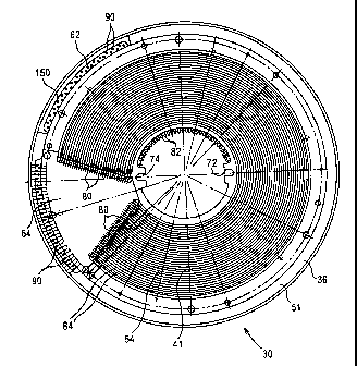
Refer now to Figures 2A and 2B which depict opposite sides of any one of
the electrical slip ring assemblies 30, 32, 34 but for brevity only electrical
slip
ring assembly 30 is described. The electrical slip ring assembly 30 includes
the
electrical slip ring 41 which includes two preferably identical electrical
slip ring
halves 54, 56 bonded together and two preferably identical brush block
assemblies 62, 64. The brush block assemblies 62, 64 are fixedly connected to
the flanges 51, 52, respectively and extend radially inwardly therefrom. The
electrical slip ring halves 54, 56 can be of different configurations. The
brush
block assemblies can also be of different configurations. The brush block
assemblies 62, 64 are pie shaped with one edge fixedly connected to a
corresponding flange 51, 52. Each brush block assembly 62, 64 is cantilevered
from the flange 51, 52 and so rigidity of the printed circuit board of each
brush
block assembly 62, 64 is important in order to maintain uniform contact
between
the brushes and their respective electrical slip rings. The annular body 36
and
brush block assemblies 62, 64 remain stationary relative to the housing 20
during
the operation of the electrical slip ring apparatus 10 while the electrical
slip ring
assemblies 30, 32, 34 rotate. The brush block assemblies 62, 64 are located on
opposite sides of the composite electrical slip ring 50 and are angularly
spaced
from each other in a circumferential direction. A plurality of leads 82 are
electrically connected at an inner periphery of the electrical slip ring 41 to
a rotary
member (not shown). Each electrical slip ring half 54, 56 has a plurality of
concentric radially spaced electrical rings 84. Each brush block 62, 64 has a
plurality of brushes 80 and is electrically connected to a corresponding
plurality
of leads 90. The leads 90 are soldered to corresponding connecting points 150.
The electrical slip ring 50 has diametrically opposite radial slots 72, 74 for
engaging the hub 48.
Refer now to Figure 3A where a composite electrical slip ring 50 is
depicted, according to the present invention, connected to the hub 48. As
depicted in Figure 3B, the composite electrical slip ring 50 includes the two
CA 02296825 2000-01-24
-
electrical slip ring halves 54, 56 bonded together with epoxy polyamide
adhesive
to form the composite electrical slip ring 41. As depicted in Figure 3B, the
slip
ring halves 54, 56 have a plurality of concentric spaced electrical rings 84.
Each
ring 84 has a groove 86 for receiving a corresponding brush 80. The groove is
5 defined by a pair of side walls 89 and a radiused surface 91 connecting the
sidewalls 89. Each of the electrical slip ring halves 54, 56 has a back
surface 93,
94 to which electrical interconnecting circuits 95, 96 are located.
Refer now to Figures 4A and 4B which depict one of the brush block
assemblies 62. The brush block assembly 62 is mounted on a printed circuit
10 board 100. Because of the high circuit density of the electrical slip ring,
the brush
block 62 must also be formed with a high circuit density corresponding to the
circuit density of the electrical slip ring 41. To accommodate the high
circuit
density, the printed circuit board is preferably formed of multiple layers
(three
layers 122, 132, 142 are depicted in Figure 4B, although any number of layers
can
be used) of circuit boards each having circuit traces formed thereon.
Advantageously, the use of multiple layers between each layer of circuit
layers
provides a ground plane between each layer of circuit layers. As depicted in
Figure 4A, there are three sets of circuit traces, each connected to a
corresponding
brush 80. A first set of circuit traces 120 (indicated by solid lines) is on a
first
layer 122, a second set of circuit traces 130 (indicated by long dashed lines)
is on
a second layer 124, and a third set of circuit traces 140 (indicated by short
dashed
lines) on a third layer 142 carries an electrical signal to/from connection
points
150 on the printed circuit board 100 of the electrical slip ring apparatus 10
to/from
a corresponding brush 80. The printed circuit boards are preferably formed of
glass reinforced epoxy laminate (FR4) and are bonded together using an epoxy
polyamide cement.
As depicted in Figure 4A, printed circuit board 100 has a pie shaped
configuration having a circumferentially extending portion 155 and two
radially
inwardly extending portions 160, 162. Connection points 150 are located on the
CA 02296825 2007-05-22
11
circumferentially extending portion 155 and the brush blocks 80 are mounted to
each of the radially inwardly extending portions 160, 162 and extend
circumferentially outwardly beyond the printed circuit board 100. The leads 90
are soldered to connection points 150.
Each of the brushes 80 is electrically connected to a corresponding trace
on one of layers 122, 132, 142. As depicted in Figure 4B, brush 80 is
connected
to a trace in layer 142. The brush 80 has a leg portion 170 and a curved
portion
172 at a distal end thereof. T he curved portion 172 has a rounded surface 174
in
mechanical and electrical contact with an electrical ring 84 in the electrical
slip
ring 41. Each brush is plated with nickel plating and then gold plated.
Referring now to Figures 5A-5L, the process of manufacturing an
electrical slip ring according to the present invention is illustrated. The
process
described below is for manufacturing each of the electrical slip ring halves
54, 56
described above having densely packed electrical rings 80. It should be noted
that
any number of electrical rings can be formed on a substrate according to the
present invention although only three rings are depicted in the partial
elevational
side views of Figures 5A-5L for ease of discussion.
A double sided copper laminate is first formed, although as depicted in
Figure 5A, only one copper layer is depicted on which the electrical rings are
formed. The electrically interconnecting circuits are not described for
clarity.
As depicted in Figure 5A, a substrate 200 has a copper layer 2101aminated
thereon.
As depicted in Figure 5B, a plurality of holes 240 are drilled through the
substrate
200 and the copper layer 210. The copper layer 210 is then coated with a
photosensitive polymer and exposed to intense ultraviolet light through a
photographic negative. The other side is similarly exposed to form the
electrical interconnections. The photosensitive polymer is then developed and
unexposed areas of the resist are selectively dissolved away with a solvent
leaving rings of developed resist.
CA 02296825 2000-01-24
12 -
As depicted in Figure 5C, the holes 240 are plated with an electrically
conductive material utilizing plated through holes processes and/or by filling
the
holes with an electrically conductive material, such as silver filled epoxy.
As
depicted in Figure 5D, multiple layers of photoresist 252, 254, 256 are
applied to
the copper layer 210. Photoresist is again applied to both sides of the slip
ring
circuit boards. Although not depicted in. Figure 5, a single layer of resist
is
applied to the electrical interconnects.
As depicted in Figure 5E, the multiple layers of photoresist 252, 254, 256
are then exposed with ultraviolet light through a phototool containing
multiple
concentric rings creating slots 262, 264, 266 for rings. As depicted in Figure
5F
after the image is developed, copper is then electroformed up between the
concentric rings of photoresist to form the copper rings 272, 274, 276. As
depicted in Figure 5G, after the resist between the electroformed rings is
removed,
the electroformed the electroformed rings are subsequently separated by
etching
away the thin layer of copper between the base of the rings, thereby
electrically
isolating the rings 272, 274, 276, as depicted in Figure 5H. As depicted in
Figure
51, the rings 272, 274, 276 are lightly sanded to flatten the top surface of
the rings.
A layer of photoresist 280 is applied to the sanded top surface of the rings.
As
depicted in Figure 5J, the photo resist 280 is developed to expose the top
surface
of the rings. As depicted in Figure 5K, the grooves 86 are etched into the top
surface of each of the rings 272, 274, 276. As depicted in Figure 5L, the
layer of
developed photoresist 280 is removed and the rings 272, 274, 276 are ready for
nickel and gold plating.
The rings 272, 274, 276 include grooves 86 that are approximately 0.008-
0.010 inches wide. The rings 272, 274, 276 have a thickness of between
approximately 0.012-0.014 inches. The rings 272, 274, 276 can be as close as
0.070 inches apart.
CA 02296825 2000-01-24
13
When the slip ring 41 is mated with brush block assemblies, it is important
that the brush pressure be consistent over repeated cycling through the
operational
temperature range of -54 C to +60 C.
To maintain boundary lubrication at low temperatures, there must be a
lubricant placed on the electrical slip rings in the grooves 86 which must
have
fluid viscosity remaining low enough to prevent the viscosity/velocity product
from reaching some critical value at which point the hydrodynamic lift will
cause
the contacts to separate. The critical value is a function of lubricant
viscosity and
lubricant quantity. Even though the quantity of lubricant required for
boundary
lubrication is smaller than that needed for full film lubrication, to a
degree, the
greater the quantity of lubricant present, the longer will be the life of the
slip ring.
But the greater the quantity, the easier it is for the lubricating mechanism
to
change from boundary lubricant to hydrodynamic lubrication, as the lubricant
viscosity increases. Enough lubricant must be present, but not too much
lubricant. Adding to the dilemma, fluids at work at very low temperatures are
so
volatile at room temperature (and higher) that they vaporize in a relatively
short
time. To reduce friction, a lubricant is used between the contact services and
are
coated with a lower molecular weight linear perfluoropolyether fluid or "Z"
fluid,
which have much improved viscosity indices (two to three times that of
conventional fluid lubricants) and low vapor pressures, pennitting operation
over
wider temperature ranges. Excessive wear can cause electrical noise and other
electrical problems.
It should now be apparent that an electrical slip has been described that
achieves high bandwidth. The present invention allows a ground plane between
each layer of circuits, allows adjustment of ring and ground separations to
minimize crosstalk and impedance mismatch, allows use of lubricants that
remain
fluid at low temperatures and provide adequate lubricity in low quantities,
minimizes contamination of the materials during the ring buildup process that
CA 02296825 2000-01-24
14
might cause high noise, and prevents formation of corrosion products on ring
sidewalls through the use of a nickel barrier coat.
It will be readily seen by one of ordinary skill in the art that the present
invention fulfills all of the objects set forth above. After reading the
foregoing
specification, one of ordinary skill will be able to affect various changes,
substitutions of equivalents and various other aspects of the invention as
broadly
disclosed herein. It is therefore intended that the protection granted hereon
be
limited only by the definition contained in the appended claims and
equivalents
thereof.